

查询LMC567供应商
LMC567
Low Power Tone Decoder
LMC567 Low Power Tone Decoder
June 1999
General Description
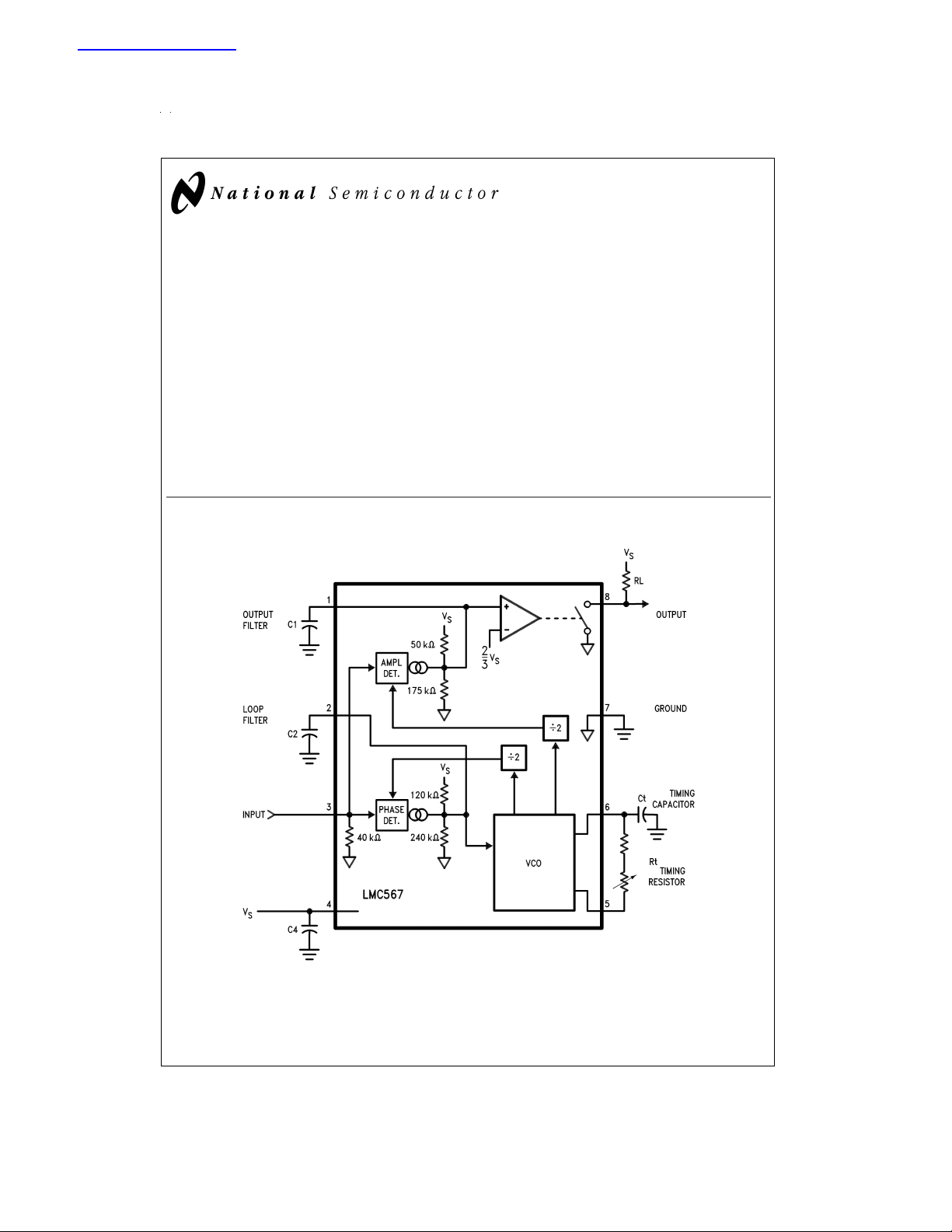
The LMC567 is a low power general purpose LMCMOS
tone decoder which is functionally similar to the industry
standard LM567. It consists of a twice frequency
voltage-controlled oscillator (VCO) and quadrature dividers
which establish the reference signals for phase and amplitude detectors. The phase detector and VCO form a
phase-locked loop (PLL) which locks to an input signal frequency which is within the control range of the VCO. When
the PLL is locked and the input signal amplitude exceeds an
internally pre-set threshold, a switch to ground is activated
on the output pin. External components set up the oscillator
to run at twice the input frequency and determine the phase
and amplitude filter time constants.
Block Diagram (with External Components)
Features
n Functionally similar to LM567
™
n 2V to 9V supply voltage range
n Low supply current drain
n No increase in current with output activated
n Operates to 500 kHz input frequency
n High oscillator stability
n Ground-referenced input
n Hysteresis added to amplitude comparator
n Out-of-band signals and noise rejected
n 20 mA output current capability
DS008670-1
Order Number LMC567CM or LMC567CN
See NS Package Number M08A or N08E
LMCMOS™is a trademark of National Semiconductor Corp.
© 1999 National Semiconductor Corporation DS008670 www.national.com
Absolute Maximum Ratings (Note 1)
If Military/Aerospace specified devices are required,
please contact the National Semiconductor Sales Office/
Distributors for availability and specifications.
Input Voltage, Pin 3 2 V
Supply Voltage, Pin 4 10V
Output Voltage, Pin 8 13V
Voltage at All Other Pins Vs to Gnd
Output Current, Pin 8 30 mA
Package Dissipation 500 mW
Operating Temperature Range (T
) −25˚C to +125˚C
A
p–p
Storage Temperature Range −55˚C to +150˚C
Soldering Information
Dual-In-Line Package
Soldering (10 sec.) 260˚C
Small Outline Package
Vapor Phase (60 sec.) 215˚C
Infrared (15 sec.) 220˚C
See AN-450 “Surface Mounting Methods and Their Effect
on Product Reliability” for other methods of soldering
surface mount devices.
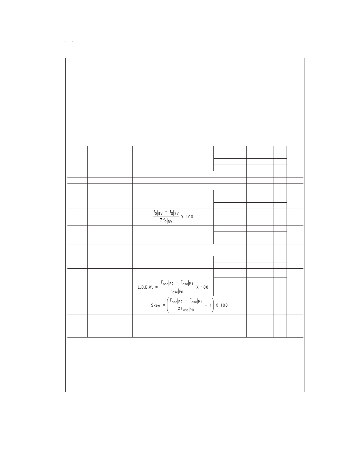
Electrical Characteristics
Test Circuit, T
=
A
Symbol Parameter Conditions Min Typ Max Units
I4 Power Supply
Current
V3 Input D.C. Bias 0 mVdc
R3 Input Resistance 40 kΩ
I8 Output Leakage 1 100 nAdc
f
∆f
V
∆V
0
0
in
Center Frequency,
÷
2
F
osc
Center Frequency
Shift with Supply
Input Threshold Set Input Frequency Equal to f
Input Hysteresis Starting at Input Threshold, Decrease Input
in
V8 Output ’Sat’ Voltage Input Level
L.D.B.W. Largest Detection
Bandwidth
∆BW Bandwidth Skew
25˚C, V
=
s
#
5V, RtCt
2, Sw. 1 Pos. 0, and no input, unless otherwise noted.
#
1, Quiescent
RtCt
or Activated
#
RtCt
2, Measure Oscillator
Frequency and Divide by 2
Measured Above, Increase Input Level
Until Pin 8 Goes Low.
Level Until Pin 8 goes High.
>
Threshold
Choose RL for Specified I8
Measure F
Pos. 0, 1, and 2;
with Sw. 1 in
osc
=
V
2V 0.3
s
=
5V 0.5 0.8
s
=
V
9V 0.8 1.3
s
=
V
2V 98
s
=
5V 92 103 113
s
=
V
9V 105
s
1.0 2.0
=
2V 11 20 27
0
V
s
=
5V 17 30 45
s
=
V
9V 45
s
mAdcV
kHzV
%
/V
mVrmsV
1.5 mVrms
I8=2 mA 0.06 0.15
I8=20 mA 0.7
=
V
2V
s
=
V
s
=
V
s
5V
9V
71115
11 14 17
15
0±1.0
Vdc
%
%
f
max
V
in
Note 1: Absolute Maximum Ratingsindicatelimitsbeyond which damage to the device may occur. Operating Ratings indicate conditions for which the device is functional, but do not guarantee specific performance limits. Electrical Characteristics state DC and AC electrical specifications under particular test conditions which guarantee specific performance limits. This assumes that the device is within the Operating Ratings. Specifications are not guaranteed for parameters where no limit is
given, however, the typical value is a good indication of device performance.
www.national.com 2
Highest Center
Freq.
Input Threshold at
f
max
RtCt#3, Measure Oscillator Frequency and Divide by 2
Set Input Frequency Equal to f
Increase Input Level Until Pin 8 goes Low.
measured Above,
max
700 kHz
35
mVrms
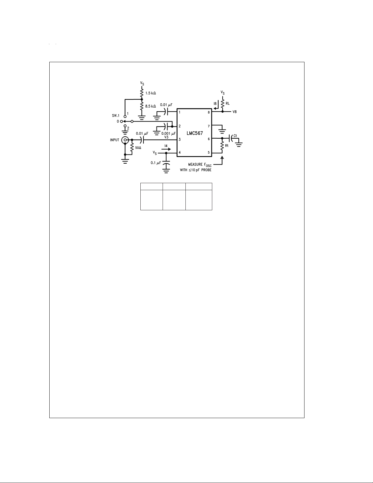
Test Circuit
RtCt Rt Ct
#
1 100k 300 pF
#
2 10k 300 pF
#
3 5.1k 62 pF
DS008670-2
www.national.com3
 Loading...