

查询LMC555CN 供应商
LMC555
CMOS Timer
LMC555 CMOS Timer
February 2000
General Description
The LMC555 is a CMOS version of the industry standard
555 series general purpose timers. In addition to the standard package(SOIC, MSOP, and MDIP) the LMC555 is also
available in achip sized package(8 Bump micro SMD) using
National’s micro SMD package technology. The LMC555 offers the same capability of generating accurate time delays
and frequencies as the LM555 but with much lower power
dissipation and supply current spikes. When operated as a
one-shot, the time delay is precisely controlled by a single
external resistor and capacitor. In the stable mode the oscillation frequency and duty cycle are accurately set by two external resistors and one capacitor. The use of National Semiconductor’s LMCMOS
range and low supply capability.
™
process extends boththe frequency
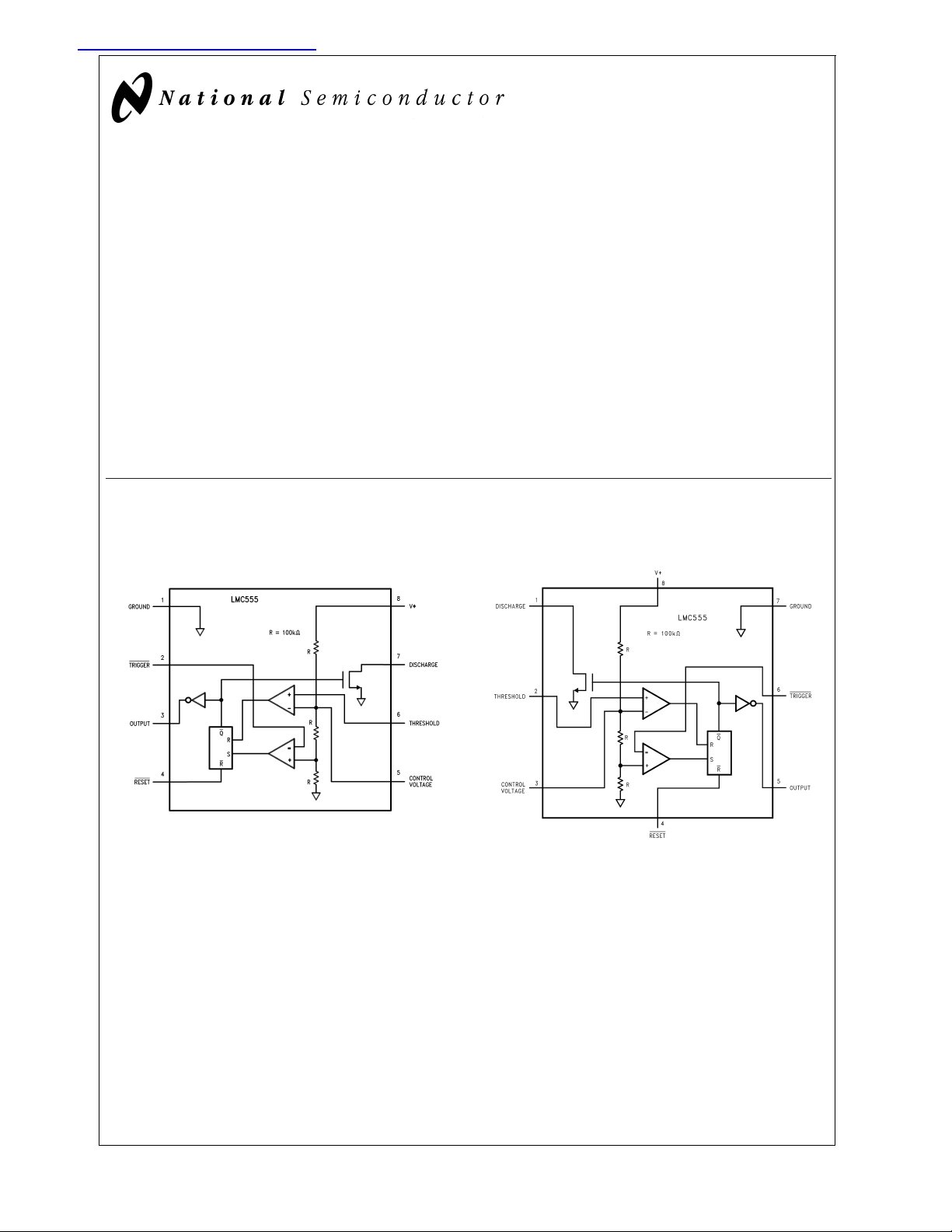
Block and Connection Diagrams
8-Pin SOIC, MSOP,
and MDIP Packages
Features
n Less than 1 mW typical power dissipation at 5V supply
n 3 MHz astable frequency capability
n 1.5V supply operating voltage guaranteed
n Output fully compatible with TTL and CMOS logic at 5V
supply
n Tested to −10 mA, +50 mA output current levels
n Reduced supply current spikes during output transitions
n Extremely low reset, trigger, and threshold currents
n Excellent temperature stability
n Pin-for-pin compatible with 555 series of timers
n Available in 8 pin MSOP Package and 8-Bump micro
SMD package
8-Bump micro SMD
DS008669-1
Top View
Top View
(bump side down)
LMCMOS™is a trademark of National Semiconductor Corp.
© 2000 National Semiconductor Corporation DS008669 www.national.com
DS008669-9
Ordering Information
LMC555
Package Temperature Range Package Marking Transport Media NSC
Industrial
−40˚C to +85˚C
8-LeadSmall Outline
(SO)
8-Lead Mini Small
Outline (MSOP)
8-Lead Molded Dip
(MDIP)
8-Bump micro SMD LMC555CBP F1 250 Units Tape and Reel
Metronome Circuit LMC555CBPEVAL N/A N/A N/A
LMC555CM LMC555CM Rails
LMC555CMX LMC555CM 2.5k Units Tape and Reel
LMC555CMM ZC5 1k Units Tape and Reel
LMC555CMMX ZC5 3.5k Units Tape and Reel
LMC555CN LMC555CN Rails
LMC555CBPX F1 3k Units Tape and Reel
micro SMD Marking Orientation
Top View
Drawing
M08A
MUA08A
N08E
BPA08EFB
Bumps are numbered counter-clockwise
DS008669-23
www.national.com 2
LMC555
Absolute Maximum Ratings (Notes 2, 3)
If Military/Aerospace specified devices are required,
please contact theNational Semiconductor SalesOffice/
Distributors for availability and specifications.
Supply Voltage, V
Input Voltages, V
V
THRESH
Output Voltages, V
Output Current I
Storage Temperature Range −65˚C to +150˚C
Soldering Information
MDIP Soldering (10 seconds) 260˚C
SOIC, MSOP Vapor Phase (60
sec) 215˚C
+
TRIG,VRES,VCTRL
O,VDIS
O,IDIS
15V
,
−0.3V to VS+ 0.3V
15V
100 mA
Operating Ratings(Notes 2, 3)
Termperature Range −40˚C to +85˚C
Thermal Resistance (θ
SO, 8-lead Small Outline 169˚C/W
MSOP, 8-lead Mini Small
Outline 225˚C/W
MDIP, 8-lead Molded Dip 111˚C/W
8-Bump micro SMD 220˚C/W
Maximum Allowable Power
@
Dissipation
25˚C
MDIP-8 1126mW
SO-8 740mW
MSOP-8 555mW
8 Bump micro SMD 568mW
) (Note 2)
JA
SOIC, MSOP Infrared (15 sec) 220˚C
Note: See AN-450 “Surface Mounting Methods and Their Effect on Product
Reliability” for other methods of soldering surface mount devices.
Electrical Characteristics (Notes 1, 2)
Test Circuit, T=25˚C, all switches open, RESET to V
Symbol Parameter Conditions Min Typ Max Units
I
S
V
CTRL
V
DIS
V
OL
V
OH
V
TRIG
I
TRIG
V
RES
I
RES
I
THRESH
I
DIS
Supply Current V
Control Voltage V
Discharge Saturation
Voltage
Output Voltage (Low) V
Output Voltage
(High)
Trigger Voltage V
Trigger Current V
Reset Voltage V
Reset Current V
Threshold Current V
Discharge Leakage V
=
1.5V
S
=
5V
V
S
=
12V
V
S
=
1.5V
S
=
5V
V
S
=
12V
V
S
=
V
1.5V, I
S
=
5V, I
V
S
=
1.5V, I
S
=
5V, I
V
S
=
12V, I
V
S
=
V
1.5V, I
S
=
5V, I
V
S
=
12V, I
V
S
=
1.5V
S
=
12V
V
S
=
5V 10 pA
S
=
1.5V (Note 4)
S
=
12V
V
S
=
5V 10 pA
S
=
5V 10 pA
S
=
12V 1.0 100 nA
S
t Timing Accuracy SW 2, 4 Closed
=
V
1.5V
S
=
5V
V
S
=
12V
V
S
∆t/∆V
Timing Shift with Supply V
S
∆t/∆T Timing Shift with
Temperature
f
A
f
MAX
t
R,tF
Astable Frequency SW 1, 3 Closed, V
Maximum Frequency Max. Freq. Test Circuit, V
Output Rise and
Fall Times
=
5V
S
=
V
5V
S
−40˚C ≤ T ≤ +85˚C
Max. Freq. Test Circuit
=
5V, C
V
S
unless otherwise noted
S
0.8
2.9
7.4
=
1mA
DIS
=
10 mA
DIS
=
1mA
O
=
8mA
O
=
50 mA
O
=
O
O
=
=
O
−0.25 mA
−2 mA
−10 mA
1.0
4.4
10.5
0.4
3.7
0.4
0.4
0.9
1.0
1.0
±
1V 0.3
=
12V 4.0 4.8 5.6 kHz
S
=
5V 3.0 MHz
S
=
10 pF
L
(Limits)
50
100
150
1.0
3.3
8.0
75
150
0.2
0.3
1.0
150
250
400
1.2
3.8
8.6
150
300
0.4
0.6
2.0
µA
V
mV
V
1.25
4.7
V
11.3
0.5
4.0
0.7
0.75
1.1
1.1
1.1
0.6
4.3
1.0
1.1
1.25
1.20
1.25
V
V
ms
%
75 ppm/˚C
15 ns
/V
www.national.com3
Electrical Characteristics (Notes 1, 2)
Test Circuit, T=25˚C, all switches open, RESET to V
LMC555
Symbol Parameter Conditions Min Typ Max Units
t
PD
Trigger Propagation Delay V
=
5V, Measure Delay
S
from Trigger to Output
Note 1: All voltages are measured with respect to the ground pin, unless otherwise specified.
Note 2: Absolute Maximum Ratings indicate limits beyond which damagetothedevicemayoccur. Operating Ratings indicate conditions for whichthedeviceisfunc-
tional, but donotguaranteespecificperformancelimits.Electrical Characteristics state DC and AC electrical specifications under particular test conditions which guarantee specific performance limits. This assumes that the device is within the Operating Ratings. Specifications are not guaranteed for parameters where no limit is
given, however, the typical value is a good indication of device performance.
Note 3: See AN-450 for other methods of soldering surface mount devices, and also AN-1112 for micro SMD considerations.
Note 4: If the RESET pin is to be used at temperatures of −20˚C and below V
Note 5: For device pinout please refer to table 1
unless otherwise noted (Continued)
S
is required to be 2.0V or greater.
S
100 ns
(Limits)
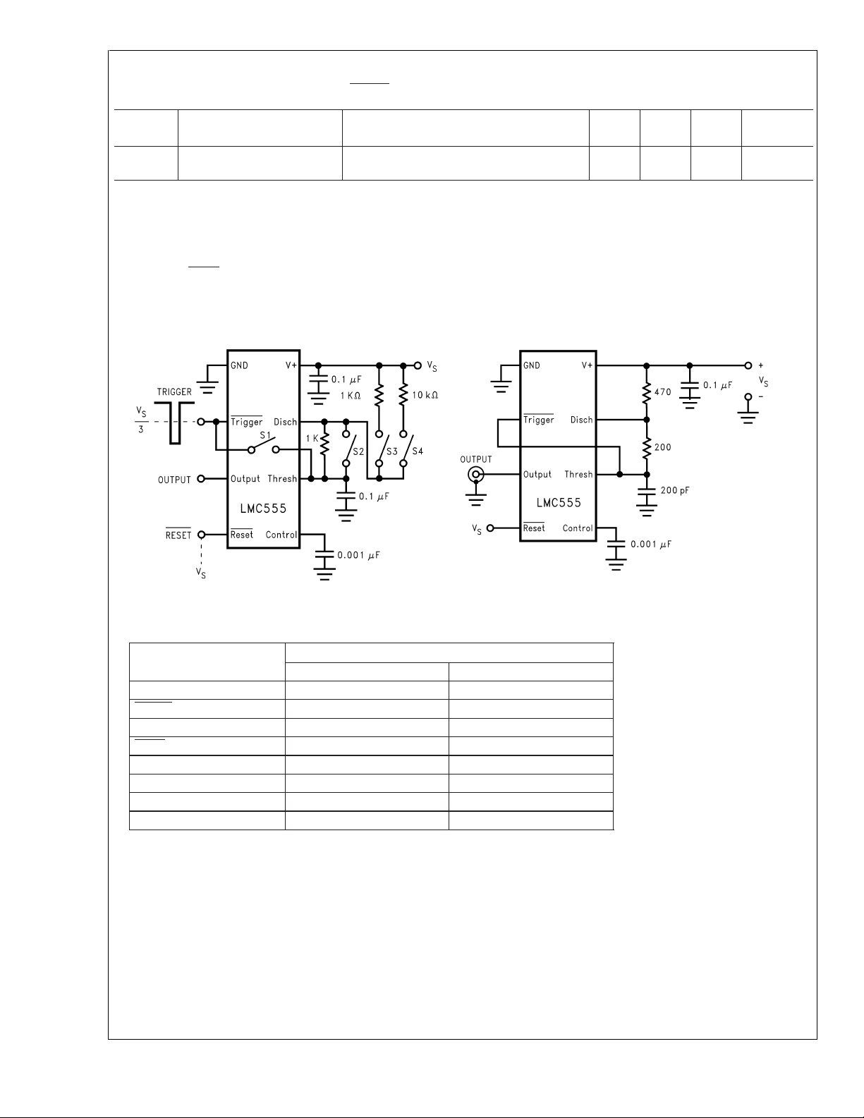
Test Circuit (Note 5)
DS008669-2
Maximum Frequency Test Circuit (Note 5)
TABLE 1. Package Pinout Names vs. Pin Function
Pin Function Package Pin numbers
8-Pin SO,MSOP, and MDIP 8-Bump micro SMD
GND 1 7
Trigger
26
Output 3 5
Reset
44
Control Voltage 5 3
Threshold 6 2
Discharge 7 1
+
V
88
DS008669-3
www.national.com 4
 Loading...