

National Semiconductor LMC555 Technical data
LMC555
CMOS Timer
LMC555 CMOS Timer
October 2003
General Description
The LMC555 is a CMOS version of the industry standard
555 series general purpose timers. In addition to the standard package (SOIC, MSOP, and MDIP) the LMC555 is also
available in a chip sized package (8 Bump micro SMD) using
National’s micro SMD package technology. The LMC555
offers the same capability of generating accurate time delays
and frequencies as the LM555 but with much lower power
dissipation and supply current spikes. When operated as a
one-shot, the time delay is precisely controlled by a single
external resistor and capacitor. In the stable mode the oscillation frequency and duty cycle are accurately set by two
external resistors and one capacitor. The use of National
Semiconductor’s LMCMOS
quency range and low supply capability.
™
process extends both the fre-
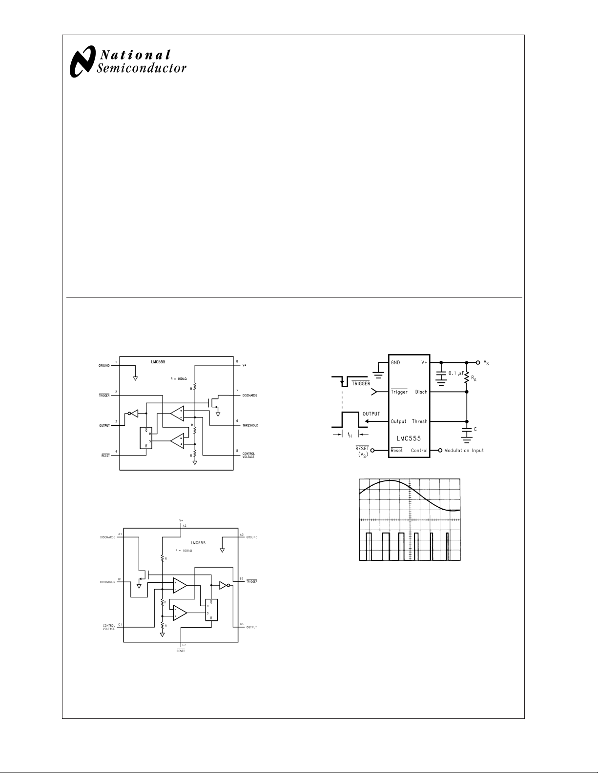
Block and Connection Diagrams
8-Pin SOIC, MSOP,
and MDIP Packages
Features
n Less than 1 mW typical power dissipation at 5V supply
n 3 MHz astable frequency capability
n 1.5V supply operating voltage guaranteed
n Output fully compatible with TTL and CMOS logic at 5V
supply
n Tested to −10 mA, +50 mA output current levels
n Reduced supply current spikes during output transitions
n Extremely low reset, trigger, and threshold currents
n Excellent temperature stability
n Pin-for-pin compatible with 555 series of timers
n Available in 8 pin MSOP Package and 8-Bump micro
SMD package
Pulse Width Modulator
00866920
Top View
8-Bump micro SMD
Top View
(Bump side down)
LMCMOS™is a trademark of National Semiconductor Corp.
© 2004 National Semiconductor Corporation DS008669 www.national.com
00866901
00866915
00866909
Ordering Information
LMC555
Note: See Mil-datasheet MNLMC555-X for specifications on the military device LMC555J/883.
Package Temperature Range Package Marking Transport Media NSC Drawing
Industrial
−40˚C to +85˚C
8-LeadSmall Outline
(SO)
8-Lead Mini Small
Outline (MSOP)
8-Lead Molded Dip
(MDIP)
8-Bump micro SMD LMC555CBP F1 250 Units Tape and Reel
LMC555CM LMC555CM Rails
LMC555CMX LMC555CM 2.5k Units Tape and Reel
LMC555CMM ZC5 1k Units Tape and Reel
LMC555CMMX ZC5 3.5k Units Tape and Reel
LMC555CN LMC555CN Rails
LMC555CBPX F1 3k Units Tape and Reel
M08A
MUA08A
N08E
BPA08EFB
www.national.com 2
LMC555
Absolute Maximum Ratings (Notes 2, 3)
If Military/Aerospace specified devices are required,
please contact the National Semiconductor Sales Office/
Distributors for availability and specifications.
Supply Voltage, V
Input Voltages, V
V
CTRL,VTHRESH
Output Voltages, V
Output Current I
+
TRIG,VRES
O,VDIS
O,IDIS
,
−0.3V to VS+ 0.3V
Storage Temperature Range −65˚C to +150˚C
Soldering Information
MDIP Soldering (10 seconds) 260˚C
SOIC, MSOP Vapor Phase (60
sec) 215˚C
SOIC, MSOP Infrared (15 sec) 220˚C
Note: See AN-450 “Surface Mounting Methods and Their Effect on Product
Reliability” for other methods of soldering surface mount devices.
15V
15V
100 mA
Operating Ratings(Notes 2, 3)
Termperature Range −40˚C to +85˚C
Thermal Resistance (θ
SO, 8-lead Small Outline 169˚C/W
MSOP, 8-lead Mini Small
Outline 225˚C/W
MDIP, 8-lead Molded Dip 111˚C/W
8-Bump micro SMD 220˚C/W
Maximum Allowable Power
Dissipation
@
25˚C
MDIP-8 1126mW
SO-8 740mW
MSOP-8 555mW
8 Bump micro SMD 568mW
) (Note 2)
JA
Electrical Characteristics (Notes 1, 2)
Test Circuit, T = 25˚C, all switches open, RESET to V
Symbol Parameter Conditions Min Typ Max Units
I
S
V
CTRL
V
DIS
V
OL
V
OH
V
TRIG
I
TRIG
V
RES
I
RES
I
THRESH
I
DIS
Supply Current VS= 1.5V
=5V
V
S
= 12V
V
S
Control Voltage VS= 1.5V
=5V
V
S
= 12V
V
S
Discharge Saturation Voltage VS= 1.5V, I
= 5V, I
V
S
Output Voltage (Low) VS= 1.5V, IO=1mA
= 5V, IO=8mA
V
S
= 12V, IO=50mA
V
S
Output Voltage
(High)
VS= 1.5V, IO= −0.25 mA
= 5V, IO=−2mA
V
S
= 12V, IO= −10 mA
V
S
Trigger Voltage VS= 1.5V
= 12V
V
S
Trigger Current VS=5V 10 pA
Reset Voltage VS= 1.5V (Note 4)
= 12V
V
S
Reset Current VS=5V 10 pA
Threshold Current VS=5V 10 pA
Discharge Leakage VS= 12V 1.0 100 nA
t Timing Accuracy SW 2, 4 Closed
VS= 1.5V
=5V
V
S
= 12V
V
S
∆t/∆V
∆t/∆T Timing Shift with
f
A
f
MAX
Timing Shift with Supply VS=5V±1V 0.3 %/V
S
V
=5V
S
Temperature
−40˚C ≤ T ≤ +85˚C
Astable Frequency SW 1, 3 Closed, VS= 12V 4.0 4.8 5.6 kHz
Maximum Frequency Max. Freq. Test Circuit, VS= 5V 3.0 MHz
unless otherwise noted
S
=1mA
DIS
=10mA
DIS
0.8
2.9
7.4
1.0
4.4
10.5
0.4
3.7
0.4
0.4
0.9
1.0
1.0
(Limits)
50
100
150
1.0
3.3
8.0
75
150
0.2
0.3
1.0
150
250
400
1.2
3.8
8.6
150
300
0.4
0.6
2.0
µA
V
mV
V
1.25
4.7
V
11.3
0.5
4.0
0.7
0.75
1.1
1.1
1.1
0.6
4.3
1.0
1.1
1.25
1.20
1.25
V
V
ms
75 ppm/˚C
www.national.com3
 Loading...