

National Semiconductor LMC1992 Technical data
查询LMC1992供应商
LMC1992 Digitally-Controlled Stereo Tone and Volume
Circuit with Four-Channel Input-Selector
December 1994
LMC1992 Digitally-Controlled Stereo Tone and
Volume Circuit with Four-Channel Input Selector
General Description
The LMC1992 is a monolithic integrated circuit that provides
four stereo inputs, bass and treble tone controls, and volume, balance, and front-rear fader controls. These functions
are digitally controlled through a three-wire communication
interface. All of the LMC1992s functions are achieved with
only three external capacitors per channel. It is designed for
line level input signals (300 mV
b
2V) and has a maximum
gain of 0 dB.
The internal design is optimized for external capacitors having values of 0.1 mF or less. This allows the use of chip
capacitors for coupling and tone control functions.
Low noise and distortion result from using analog switches
and thin-film silicon-chromium resistor networks in the signal path.
Volume and fader are at minimum and tone controls are flat
when supply voltage is first applied.
Additional tone control can be achieved using the LMC835
stereo 7-band graphic equalizer connected to the
LMC1992’s select-out/select-in external processor loop.
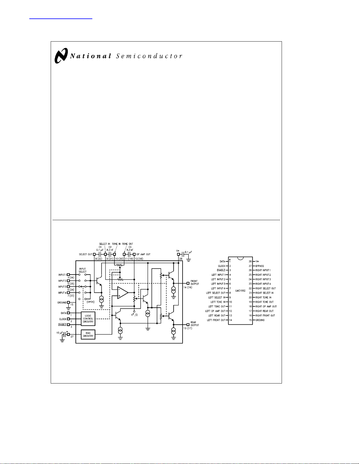
Block and Connection Diagrams
Features
Y
Low noise and distortion
Y
Four stereo inputs
Y
40 volume levels including mute
Y
20 fader levels
Y
All attenuators havea2dBofattenuation per step
Y
Front/back fade control
Y
External processor loop
Y
Only three external components per channel
Y
Serial programmable: standard MICROWIRE
TM
interface
Y
Single supply operation: 6V to 12V supply voltage
Y
Protection address (similar to DS8906)
Y
DC-coupled inputs
Y
Single supply operation
Applications
Y
Automotive audio systems
Y
Sound reinforcement systems
Y
Home entertainmentÐstereo television and music reproduction systems
Y
Electronic music (MIDI)
Order Number LMC1992CCN
TL/H/10789– 2
See NS Package Number N28B
Left channel shown. Pin numbers in parentheses are for the right channel.
DNRÉis a registered trademark of National Semiconductor Corporation.
TM
COPS
and MICROWIRETMare trademarks of National Semiconductor Corporation.
C
1995 National Semiconductor Corporation RRD-B30M75/Printed in U. S. A.
TL/H/10789
TL/H/10789– 1
Absolute Maximum Ratings (Notes 1 and 2)
If Military/Aerospace specified devices are required,
please contact the National Semiconductor Sales
Office/Distributors for availability and specifications.
a
Supply Voltage (V
Voltage at Any Pin GNDb0.2V to V
b
GND) 15V
a
a
0.2V
Input Current at Any Pin (Note 3) 5 mA
Package Input Current (Note 3) 20 mA
Power Dissipation (Note 4) 500 mW
Junction Temperature 125
Electrical Characteristics The following specifications apply for V
channel 1, volume
e
0 dB, basse0 dB, treblee0 dB, and faderse0 dB unless otherwise specified. All limits T
§
25§C.
Symbol Parameter Conditions
I
S
V
V
Supply Current 27.0 mA (max)
Input Voltage Clipping Level (1.0% THD),
IN
Output Voltage Clipping Level (1.0% THD),
OUT
Select Out (Pins 8, 22)
Outputs (Pins 13, 14, 16, 17)
THD Total Harmonic Distortion All Four Channels
Volume Attenuator at 0 dB, Input Level 0.3 V
Volume Attenuator at
E
E
R
R
Output Noise All Four Channels CCIR/ARM Filter, R
nOUT
Output Noise All Four Channels CCIR/ARM Filter, R
nOUT
DC Output Impedance Pins 8, 22 100 150 X (max)
OUT
DC Input Impedance Pins 4, 5, 6, 7, 23, 24, 25, 26 2 MX
IN
Volume Attenuatoreb80 dB
Pins 13, 14, 16, 17 80 120 X (max)
Volume Attenuator Range Pins 16, 17; Volume Attenuation at
0101110100X (0 dB); (Absolute Gain)
01011000000 (80 dB); (Relative to Attenuation at
Volume Step Size All Volume Attenuation Settings from 01011001010 2.0 0.7 dB (min)
(60 dB) to 0101110100X (0 dB) (Note 9) 4.3 dB (max)
Channel-to-Channel Volume Fader Attenuation from 1XXX000000
Tracking Error (40 dB) to 1XXX1010X (0 dB)
Fader Attenuation Range Pins 16, 17; Fader Attenuation at
011XXX1010X (0 dB); (Absolute Gain)
011XXX00000 (40 dB); (Relative to Attenuation at
Fader Step Size All Fader Attenuation Settings from 011XXX00000 2.0 1.0 dB (min)
(40 dB) to 011XXX1010X (0 dB) (Note 10) 4.5 dB (max)
Storage Temperature
Lead Temperature
N Package, Soldering, 10 sec.
ESD Susceptibility (Note 5) 2000V
Pins 9, 10, 11, 19, 20, 21 850V
Operating Ratings (Notes 1 and 2)
Temperature Range T
C
LMC1992CCN 0§CsT
Supply Voltage Range (V
b
20 dB, Input Level 0.6 V
the 0 dB setting)
the 0 dB setting)
a
b
Vb) 6Vto12V
a
e
8V, f
e
1 kHz, input signal applied to
IN
Typical Limit Units
(Note 6) (Note 7) (Limit)
2.3 2.0 V
1.2 0.65 V
rms
e
0X 6.5 30.0 mV
S
e
0X
S
0.15 0.3 % (max)
0.03 0.1 % (max)
rms
5.0 20.0 mV
b
1.0
b
80.0 75.0 dB (min)
g
b
0.5
1.0
g
b
40 38.0 dB (min)
b
65§Ctoa150§C
a
260§C
s
s
T
MIN
T
A
MAX
s
70§C
A
e
T
A
J
(min)
rms
(min)
rms
(max)
rms
(max)
rms
1.5 dB (max)
1.0 dB (max)
1.5 dB (max)
e
2
a
Electrical Characteristics The following specifications apply for V
channel 1, volume
e
0 dB, basse0 dB, treblee0 dB, and faderse0 dB unless otherwise specified. All limits T
e
25§C. (Continued)
Symbol Parameter Conditions
Bass Gain Range f
Bass Tracking Error f
Bass Step Size f
Treble Gain Range f
Treble Tracking Error f
Treble Step Size f
Frequency Response
Channel Separation V
Input-Input Isolation V
PSRR Power Supply Rejection Ratio V
f
CLK
V
IN(1)
V
IN(0)
Note 1: Absolute Maximum Ratings indicate limits beyond which damage to the device may occur. Operating Ratings indicate conditions for which the device is
functional, but do not guarantee specific performance limits. For guaranteed specifications and test conditions, see the Electrical Characteristics. The guaranteed
specifications apply only for the test conditions listed. Some performance characteristics may degrade when the device is not operated under the listed test
conditions.
Note 2: All voltages are specified with respect to ground.
Note 3: When the input voltage (V
limited to 5 mA or less. The 20 mA package input current limits the number of pins that can exceed the power supply voltages with 5 mA current limit to four.
Note 4: The maximum power dissipation must be de-rated at elevated temperatures and is dictated by T
allowable power dissipation is PD
e
Note 5: Human body model; 100 pF discharged through a 1.5 kX resistor.
Note 6: Typicals are at T
Note 7: Limits are guaranteed to National’s AOQL (Average Outgoing Quality Level).
Note 8: The Input-Input Isolation is tested by driving one input and measuring the front outputs when the undriven inputs are selected.
Note 9: The Volume Step Size is defined as the change in attenuation between any two adjacent volume attenuation settings. The nominal Volume Step Size is
2 dB.
Note 10: The Fader Step Size is defined as the change in attenuation between any two adjacent fader attenuation settings. The nominal Volume Step Size is 2 dB.
Clock Frequency 1.0 0.5 MHz (max)
Logic ‘‘1’’ Input Voltage 1.3 2.0 V (min)
Logic ‘‘0’’ Input Voltage 0.4 0.8 V (max)
) at any pin exceeds the power supply voltages (V
IN
e
b
(T
125§C, and the typical junction-to-ambient thermal resistance, when board mounted, is 67§C/W.
J
JMAX
e
25§C and represent the most likely parametric norm.
e
100 Hz, Pins 14, 16
IN
e
100 Hz, Pins 14, 16
IN
e
100 Hz, Pins 14, 16 2.0 1.0 dB (min)
IN
(Relative to Previous Level) 3.0 dB (max)
e
10 kHz, Pins 14, 16
IN
e
10 kHz, Pins 14, 16
IN
e
10 kHz, Pins 14, 16 2.0 1.0 dB (min)
IN
(Relative to Previous Level) 3.0 dB (max)
b
3 dB 450 kHz
b
0.3 dB (Relative to Signal Amplitude at 1 kHz) 20 kHz (min)
e
1.0 V
IN
IN
a
100 Hz Sinewave Applied to Pin 28
TA)/iJAor the number given in the Absolute Maximum Ratings, whichever is lower. For the LMC1992CCN, T
rms
e
1.0 V
rms
e
8VDC; 100 mV
(Note 8) 90 70 dB (min)
,
P-P
k
IN
Vbor V
l
Va) the absolute value of the current at that pin should be
IN
JMAX
e
8V, f
1 kHz, input signal applied to
IN
e
e
T
A
J
Typical Limit Units
(Note 6) (Note 7) (Limit)
g
g
g
g
12
0.1
12
0.1
g
10.0 dB (min)
g
1.0 dB (max)
g
10.0 dB (min)
g
1.0 dB (max)
97 70 dB (min)
40 31 dB (min)
, wJA, and the ambient temperature TA. The maximum
JMAX
3
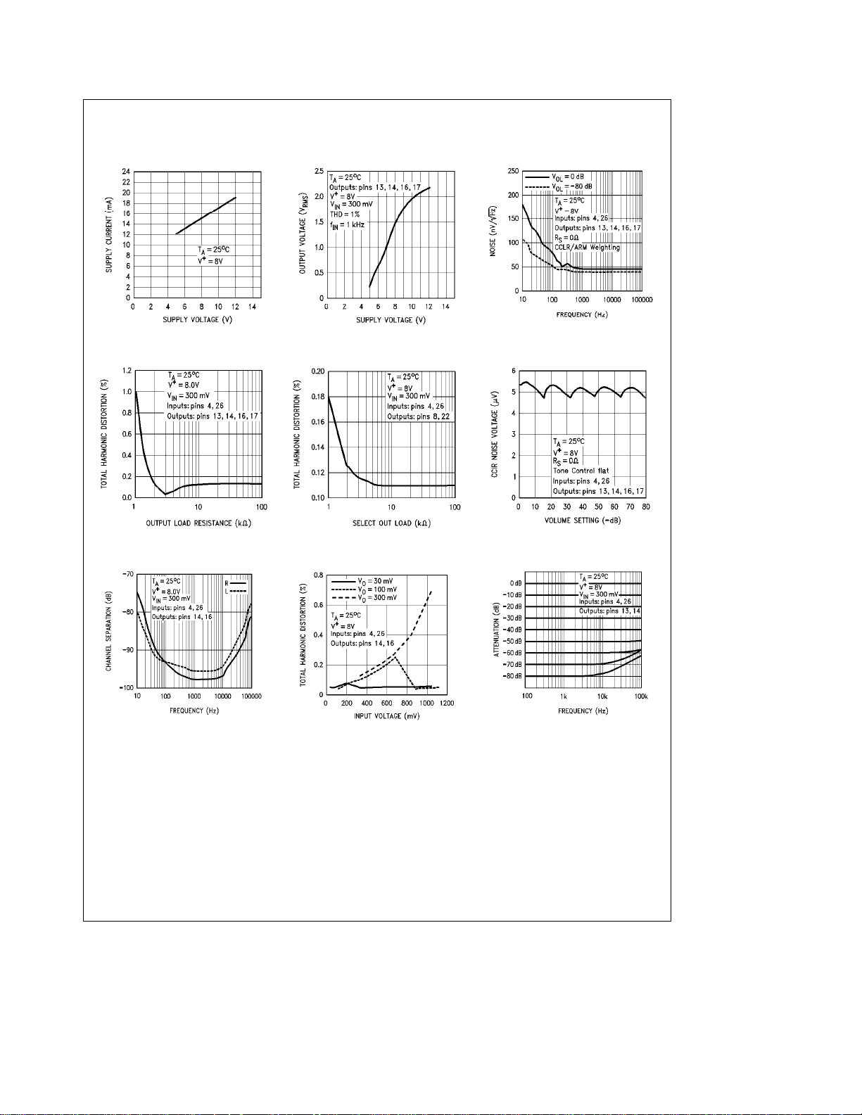
Typical Performance Characteristics
Quiescent Current vs
Supply Voltage
TL/H/10789– 3 TL/H/10789– 4
Total Harmonic Distortion
vs Output AC Load
TL/H/10789– 6 TL/H/10789– 7
Channel Separation
vs Frequency
Maximum Output Swing vs
Supply Voltage
Total Harmonic Distortion
vs Select Out AC Load
Total Harmonic Distortion
vs Input Voltage
Output Noise Voltage
vs Frequency
TL/H/10789– 5
CCIR Output Noise Voltage
vs Volume Setting
TL/H/10789– 8
Attenuation vs Frequency
TL/H/10789– 9
4
TL/H/10789– 10
TL/H/10789– 11
Typical Performance Characteristics (Continued)
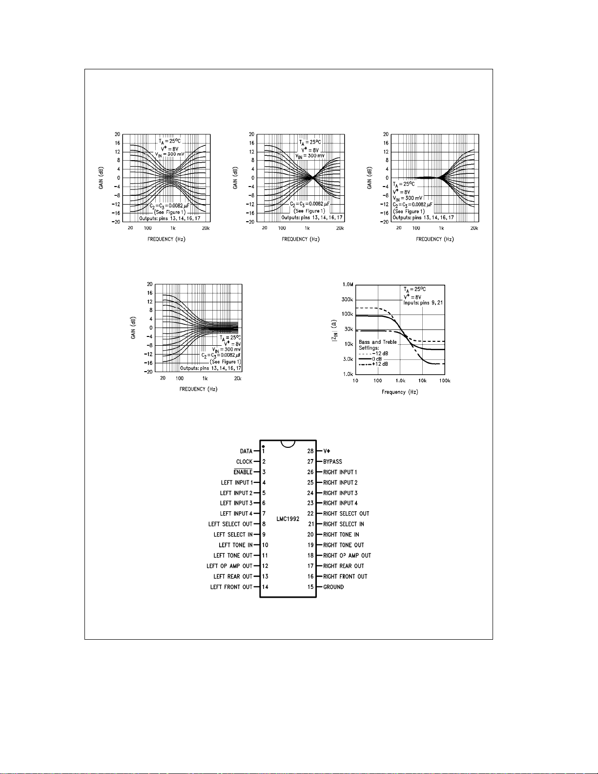
Tone Control Response
with Equal Bass and
Treble Control Settings
TL/H/10789– 12 TL/H/10789– 13 TL/H/10789– 14
Bass Tone Control
Response
Tone Control Response
with Reciprocal Bass and
Treble Control Settings
Treble Tone Control
Response
Select In Impedance
vs Frequency
Connection Diagram
TL/H/10789– 15
TL/H/10789– 16
TL/H/10789– 17
5
 Loading...