

National Semiconductor LM98640CVAL User Manual
Electronic Component Distributor. Source::Texas Instruments
P.N:LM98640CVAL Desc:EVAL BOARD FOR LM98640
Web:http://www.hotenda.cn E-mail:sales@hotenda.cn Phone:(+86) 075583794354
September 2009
Revision 1.0
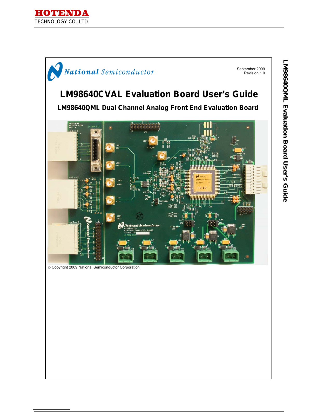
LM98640CVAL Evaluation Board User’s Guide
LM98640QML Dual Channel Analog Front End Evaluation Board
Copyright 2009 National Semiconductor Corporation
LM98640QML Evaluation Board User’s Guide
Electronic Component Distributor. Source::Texas Instruments
P.N:LM98640CVAL Desc:EVAL BOARD FOR LM98640
Web:http://www.hotenda.cn E-mail:sales@hotenda.cn Phone:(+86) 075583794354
LM98640CVAL EVALUATION BOARD USER’S GUIDE – TABLE OF CONTENTS
LM98640CVAL EVALUATION BOARD USER’S GUIDE – TABLE OF CONTENTS ......2
1.0 Introduction............................................................................................................................3
2.0 Board Assembly....................................................................................................................3
3.0 Functional Description .........................................................................................................4
3.1 Power Supply Connections .........................................................................................................................................................4
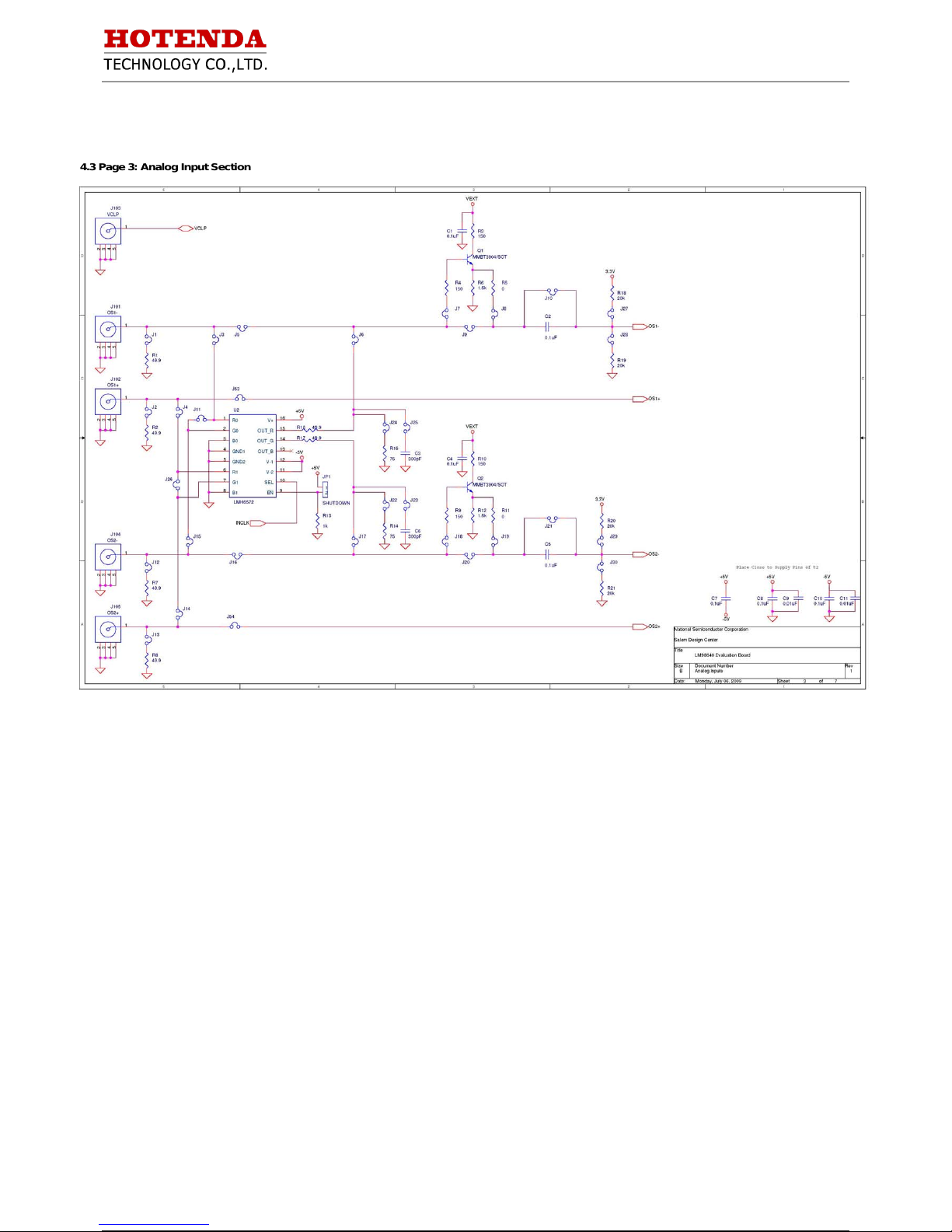
3.2 AFE Analog Input Section ...........................................................................................................................................................4
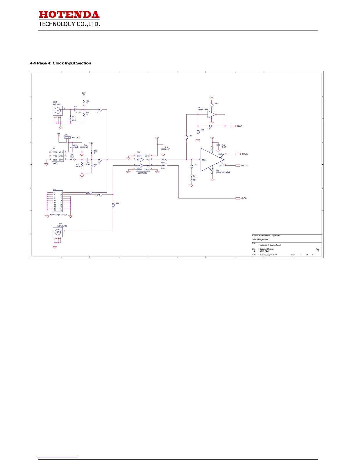
3.3 AFE Input Clock Circuit ...............................................................................................................................................................5
3.4 AFE Data Output .........................................................................................................................................................................5
3.5 AFE Serial Interface ....................................................................................................................................................................5
4.0 Schematic Drawing LM98640QML....................................................................................6
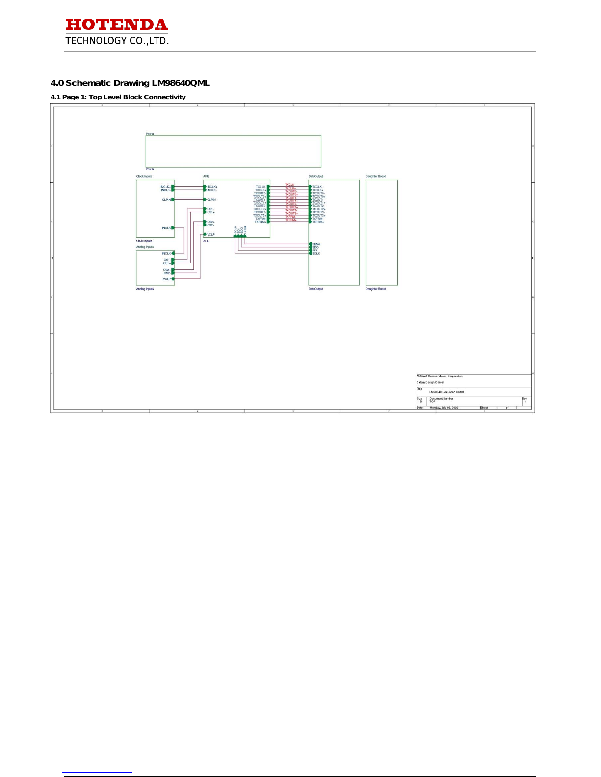
4.1 Page 1: Top Level Block Connectivity.........................................................................................................................................6
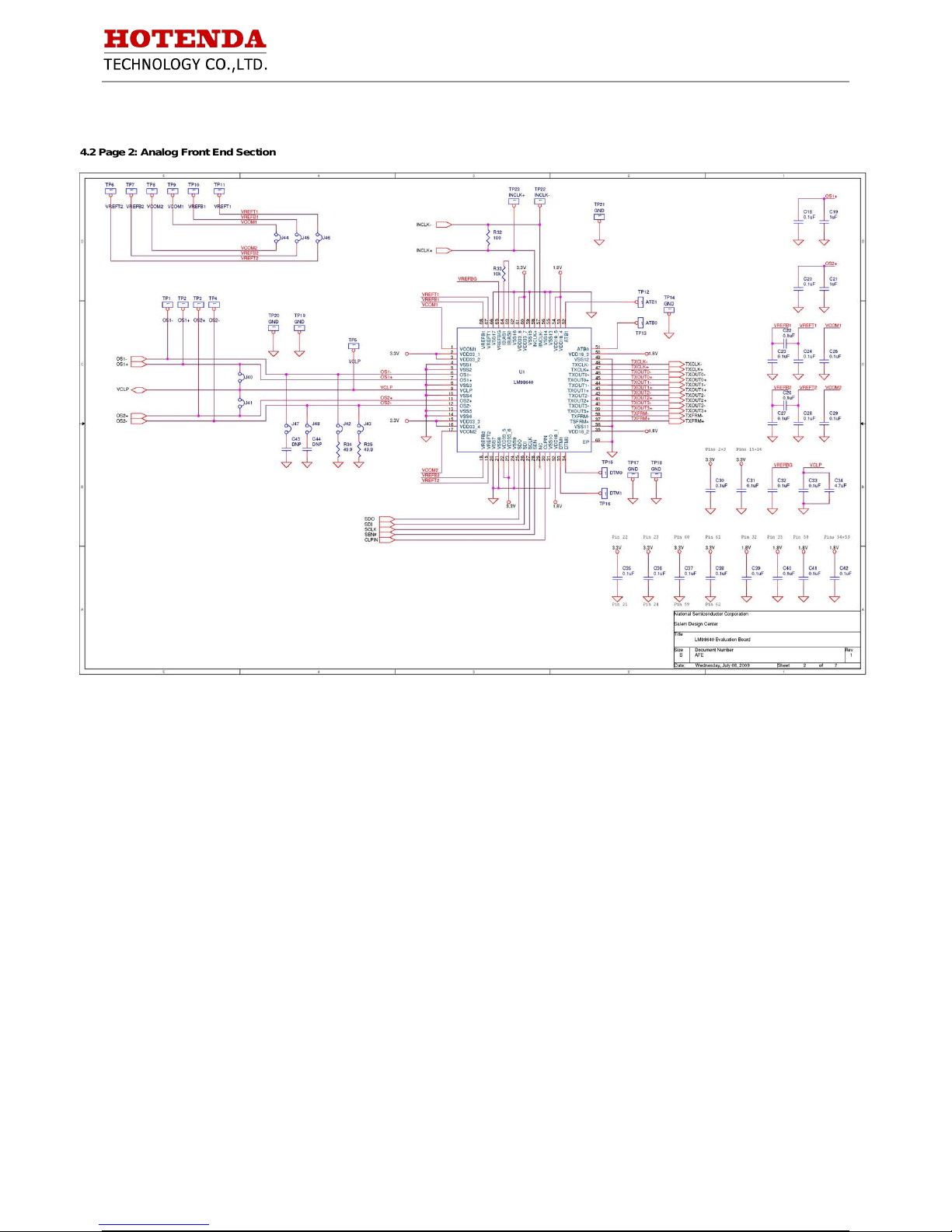
4.2 Page 2: Analog Front End Section ..............................................................................................................................................7
4.3 Page 3: Analog Input Section......................................................................................................................................................8
4.4 Page 4: Clock Input Section ........................................................................................................................................................9
4.5 Page 5: Data Output Section.....................................................................................................................................................10
4.6 Page 6: Daughter Board Connector ..........................................................................................................................................11
4.7 Page 7: Power Input Section.....................................................................................................................................................12
5.0 Evaluation Board Specifications.......................................................................................13
6.0 Bill of Materials....................................................................................................................14
7.0 Appendix A: Using the AFEval software and the Wavevision 5 Data Capture Board
......................................................................................................................................................17
7.1 Connecting the WV5 board and LM98640CVAL board for the first time...................................................................................17
7.2 Proper Board Connection and Power Sequencing....................................................................................................................17
7.3 Starting the AFEval software.....................................................................................................................................................18
7.4 LM98640QML Main Configuration Panel ..................................................................................................................................20
7.5 Register Access Panel ..............................................................................................................................................................21
7.6 AFE Timing Generator Window.................................................................................................................................................22
7.7 AFEval Data Display .................................................................................................................................................................23
8.0 Appendix B: Using the AFEval software and the Total Phase Aardvark SPI
Interface......................................................................................................................................24
8.1 Install the device drivers for the Aardvark device......................................................................................................................24
8.2 Connecting the Aardvark SPI device and LM98640CVAL board for the first time ....................................................................24
8.3 Aardvark SPI Communication via AFEval .................................................................................................................................25
9.0 Appendix C - Installing and running the AFEval software............................................26
9.1 Uninstall previous versions of AFEval Software........................................................................................................................26
9.2 Install the AFEval Software. ......................................................................................................................................................26
9.3 Microsoft .NET Framework.....................................................................................................................................................26
9.4 Windows Driver .........................................................................................................................................................................26

Electronic Component Distributor. Source::Texas Instruments
P.N:LM98640CVAL Desc:EVAL BOARD FOR LM98640
Web:http://www.hotenda.cn E-mail:sales@hotenda.cn Phone:(+86) 075583794354
1.0 Introduction
The LM98640CVAL Board is designed to allow
quick evaluation and design development of
National Semiconductor’s LM98640QML
Analog Front End. This development board is
designed to function in several different
configurations.
The primary configuration connects the
LM98640QML evaluation board to National
Semiconductor’s Wavevision 5 Data Capture
Board (WV5). The AFEval software is used to
communicate to the LM98640QML’s SPI port as
well as retrieve Data Output from the device for
display or external analysis. The present
revision of the WV5 board is limited to 30k
samples per channel. Future revisions will
allow for very deep memory capture (up to 8MB
total).
The LM98640QML evaluation board also
comes with an auxiliary adapter card. This card
allows the LM98640QML output to be routed to
one of three connectors for external data
capture and analysis. To facilitate this
configuration, a Total Phase Aardvark I2C/SPI
Host Adapter is supplied to perform the SPI
communication using the AFEval tool.
A PCB footprint for and external clock oscillator
is provided on board to allow testing without the
need of an external clock source. An SMA
connection is available for connecting an
external clock source when a variable
frequency may be desired.
The power supply for the LM98640QML and
surrounding circuitry can be made through the
WV5 board or from external bench top supplies
when the WV5 board is not being implemented.
The CCD signal inputs are made via SMD type
connections. The signals can be routed directly
to the AFE, AC coupled, emitter follower
buffered, or sent into a video multiplexer to
create a CCD type signal from a non CCD
source.
2.0 Board Assembly
The LM98640CVAL Evaluation Board comes
pre-assembled. Refer to the Bill of Materials in
Section 6 for a description of components, to
Figure 1 for major component placement and to
Section 4 for the Evaluation Board schematic.
The Evaluation Board comes as a single board
with two distinct partitions. The Evaluation
partition is on the right side, and the Adapter
Card is on the left. The two partitions should be
carefully separated to connect the AFE data
output to the desired Adapter Card connector.
Figure 1. Evaluation Board Layout
Electronic Component Distributor. Source::Texas Instruments
P.N:LM98640CVAL Desc:EVAL BOARD FOR LM98640
Web:http://www.hotenda.cn E-mail:sales@hotenda.cn Phone:(+86) 075583794354
3.0 Functional Description
The LM98640CVAL Customer Evaluation Board
schematic is shown in Section 4.
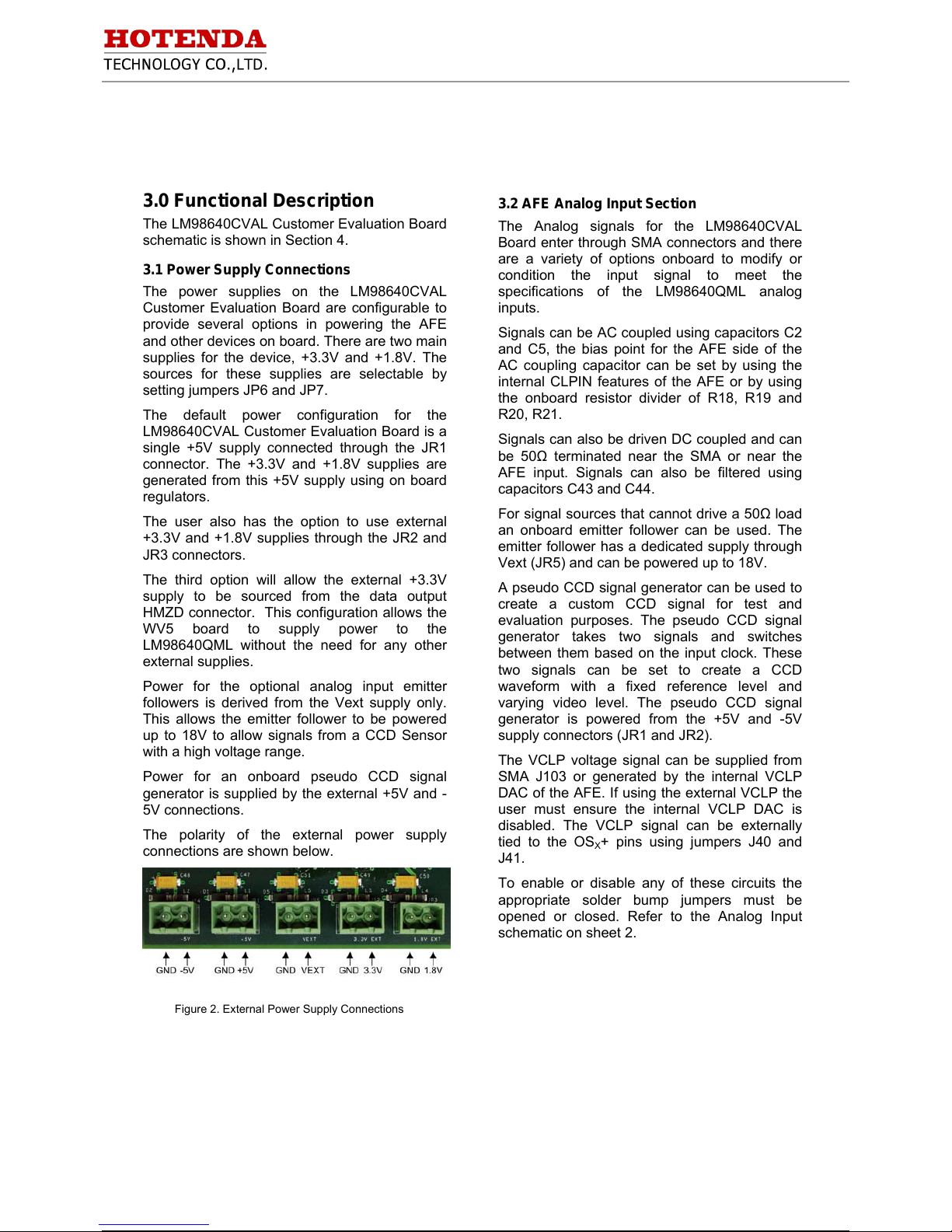
3.1 Power Supply Connections
The power supplies on the LM98640CVAL
Customer Evaluation Board are configurable to
provide several options in powering the AFE
and other devices on board. There are two main
supplies for the device, +3.3V and +1.8V. The
sources for these supplies are selectable by
setting jumpers JP6 and JP7.
The default power configuration for the
LM98640CVAL Customer Evaluation Board is a
single +5V supply connected through the JR1
connector. The +3.3V and +1.8V supplies are
generated from this +5V supply using on board
regulators.
The user also has the option to use external
+3.3V and +1.8V supplies through the JR2 and
JR3 connectors.
The third option will allow the external +3.3V
supply to be sourced from the data output
HMZD connector. This configuration allows the
WV5 board to supply power to the
LM98640QML without the need for any other
external supplies.
Power for the optional analog input emitter
followers is derived from the Vext supply only.
This allows the emitter follower to be powered
up to 18V to allow signals from a CCD Sensor
with a high voltage range.
Power for an onboard pseudo CCD signal
generator is supplied by the external +5V and -
5V connections.
The polarity of the external power supply
connections are shown below.
3.2 AFE Analog Input Section
The Analog signals for the LM98640CVAL
Board enter through SMA connectors and there
are a variety of options onboard to modify or
condition the input signal to meet the
specifications of the LM98640QML analog
inputs.
Signals can be AC coupled using capacitors C2
and C5, the bias point for the AFE side of the
AC coupling capacitor can be set by using the
internal CLPIN features of the AFE or by using
the onboard resistor divider of R18, R19 and
R20, R21.
Signals can also be driven DC coupled and can
be 50Ω terminated near the SMA or near the
AFE input. Signals can also be filtered using
capacitors C43 and C44.
For signal sources that cannot drive a 50Ω load
an onboard emitter follower can be used. The
emitter follower has a dedicated supply through
Vext (JR5) and can be powered up to 18V.
A pseudo CCD signal generator can be used to
create a custom CCD signal for test and
evaluation purposes. The pseudo CCD signal
generator takes two signals and switches
between them based on the input clock. These
two signals can be set to create a CCD
waveform with a fixed reference level and
varying video level. The pseudo CCD signal
generator is powered from the +5V and -5V
supply connectors (JR1 and JR2).
The VCLP voltage signal can be supplied from
SMA J103 or generated by the internal VCLP
DAC of the AFE. If using the external VCLP the
user must ensure the internal VCLP DAC is
disabled. The VCLP signal can be externally
tied to the OS
X
+ pins using jumpers J40 and
J41.
To enable or disable any of these circuits the
appropriate solder bump jumpers must be
opened or closed. Refer to the Analog Input
schematic on sheet 2.
Figure 2. External Power Supply Connections
Electronic Component Distributor. Source::Texas Instruments
P.N:LM98640CVAL Desc:EVAL BOARD FOR LM98640
Web:http://www.hotenda.cn E-mail:sales@hotenda.cn Phone:(+86) 075583794354
3.3 AFE Input Clock Circuit
The clock for the LM98640QML can be supplied
by one of three methods. External clocks can
be provided at either the JF1, 20 pin dual row
header on pin 1, or the J106 SMA connector.
An on board crystal oscillator (Y1) is configured
as the primary source. Changing the clock
source from the on board oscillator to one of the
external sources involves reconfiguring the
solder bump jumpers shown on schematic
page 4.
Jumper Configuration
Clock
Source
J32 J31 J33
On Board
Crystal
Oscillator Y1
short open open
External
Clock at JF1
Dual Row
Header
open open short
External
clock on
J106 SMA
Connector
open short Open
3.4 AFE Data Output
The LM98640QML LVDS output signals are run
to an HMZD connector (JF2). The Wavevision
5 Data Capture Board mates directly to this
connector.
IMPORTANT: The Wavevision 5 Data Capture
board is loaded with an FPGA image to
deserialize the LM98640QML data outputs. At
the time of this publishing, the FPGA image
supports Quad Lane output mode through the
entire operating range (i.e. 5MHz to 40MHz).
Dual Lane Mode will function from 5MHz to
35MHz. If the LM98640QML is configured in
Dual Lane Mode and the frequency is greater
than 35MHz, unexpected results may occur.
To facilitate other methods of evaluation, the
LM98640CVAL Customer Evaluation boards
come with a daughter board that has three
types of connectors: a 3M MDR Camera Link
connector, an Agilent Soft Touch connector,
and an 18 pin dual row header. To select a
particular connector the associated HMZD
connector should be connected to the HMZD
connector of the main AFE board.
Each connector of the daughter board has
termination resistors at the connector. These
resistors can be lifted from the board if the end
receiver has its own termination resistors.
3.5 AFE Serial Interface
The LM98640QML uses a 4-wire Serial
Interface to read/write the configuration
registers. The Customer Evaluation Board
provides a 2x5 pin header (JF3) to directly
interface to the AFE Serial Interface.
When the Wavevision 5 Data Capture board is
connected, the serial communication will be
automatic. The J49, J50, J51, and J52 solder
jumpers must be connected to enable the WV5
communication.
In the case where the WV5 board is not being
used, the Total Phase Aardvark I2C/SPI Host
Adapter can provide the SPI communication.
This device connects to the 2x5 pin dual row
header and a USB connection to a PC.
In either instance (WV5 or Aardvark), the
AFEval software provides the GUI interface for
the communication. See Appendix A and B for
more information on the Register Configuration
Software.
Electronic Component Distributor. Source::Texas Instruments
P.N:LM98640CVAL Desc:EVAL BOARD FOR LM98640
Web:http://www.hotenda.cn E-mail:sales@hotenda.cn Phone:(+86) 075583794354
4.0 Schematic Drawing LM98640QML
4.1 Page 1: Top Level Block Connectivity
Electronic Component Distributor. Source::Texas Instruments
P.N:LM98640CVAL Desc:EVAL BOARD FOR LM98640
Web:http://www.hotenda.cn E-mail:sales@hotenda.cn Phone:(+86) 075583794354
4.2 Page 2: Analog Front End Section
Electronic Component Distributor. Source::Texas Instruments
P.N:LM98640CVAL Desc:EVAL BOARD FOR LM98640
Web:http://www.hotenda.cn E-mail:sales@hotenda.cn Phone:(+86) 075583794354
4.3 Page 3: Analog Input Section
Electronic Component Distributor. Source::Texas Instruments
P.N:LM98640CVAL Desc:EVAL BOARD FOR LM98640
Web:http://www.hotenda.cn E-mail:sales@hotenda.cn Phone:(+86) 075583794354
4.4 Page 4: Clock Input Section
 Loading...