

August 2004
LM82
Remote Diode and Local Digital Temperature Sensor
with Two-Wire Interface
General Description
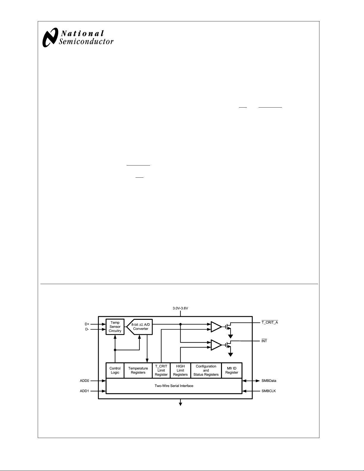
The LM82 is a digital temperature sensor with a 2 wire serial
interface that senses the voltage and thus the temperature of
a remote diode using a Delta-Sigma analog-to-digital converter with a digital over-temperature detector. The LM82
accurately senses its own temperature as well as the temperature of external devices, such as Pentium II
sors or diode connected 2N3904s. The temperature of any
ASIC can be detected using the LM82 as long as a dedicated diode (semiconductor junction) is available on the die.
Using the SMBus interface a host can access the LM82’s
registers at any time. Activation of a T_CRIT_A output occurs when any temperature is greater than a programmable
comparator limit, T_CRIT. Activation of an INT output occurs
when any temperature is greater than its corresponding
programmable comparator HIGH limit.
The host can program as well as read back the state of the
T_CRIT register and the 2 T_HIGH registers. Three state
logic inputs allow two pins (ADD0, ADD1) to select up to 9
SMBus address locations for the LM82. The sensor powers
up with default thresholds of 127˚C for T_CRIT and all
T_HIGHs. The LM82 is pin for pin and register compatible
with the LM84, Maxim MAX1617 and Analog Devices
ADM1021.
®
Proces-
Features
n Accurately senses die temperature of remote ICs, or
diode junctions
n On-board local temperature sensing
n SMBus and I
SMBus 1.1 TIMEOUT
n Two interrupt outputs: INT and T_CRIT_A
n Register readback capability
n 7 bit plus sign temperature data format, 1 ˚C resolution
n 2 address select pins allow connection of 9 LM82s on a
single bus
Key Specifications
j
Supply Voltage 3.0V to 3.6V
j
Supply Current 0.8mA (max)
j
Local Temp Accuracy (includes quantization error)
j
Remote Diode Temp Accuracy (includes quantization
error)
Applications
n System Thermal Management
n Computers
n Electronic Test Equipment
n Office Electronics
n HVAC
2
C compatible interface, supports
0˚C to +85˚C
+25˚C to +100˚C
0˚C to +125˚C
±
3.0˚C (max)
±
±
LM82 Remote Diode and Local Digital Temperature Sensor with Two-Wire Interface
3˚C (max)
4˚C (max)
Simplified Block Diagram
10129701
SMBus™is a trademark of the Intel Corporation.
®
Pentium II
is a registered trademark of the Intel Corporation.
®
I2C
is a registered trademark of the Philips Corporation.
© 2004 National Semiconductor Corporation DS101297 www.national.com
Connection Diagram
LM82
QSOP-16
Ordering Information
Typical Application
Order
Number
LM82CIMQA
LM82CIMQAX
TOP VIEW
NS Package
Number
MQA16A
(QSOP-16)
MQA16A
(QSOP-16)
10129702
Transport
Media
95 Units in
Rail
2500 Units on
Tape and Reel
www.national.com 2
10129703
Pin Descriptions
Label Pin # Function Typical Connection
floating, unconnected Left floating. PC board traces may be routed
NC 1, 5
V
CC
2
Positive Supply Voltage
Input
Diode Current Source To Diode Anode. Connected to remote discrete
D+ 3
D− 4 Diode Return Current Sink To Diode Cathode. Must float when not used.
2
ADD0–ADD1 10, 6
User-Set SMBus (I
Address Inputs
C)
GND 7, 8 Power Supply Ground Ground
Manufacturing test pins. Left floating. PC board traces may be routed
NC 9, 13, 15
INT
11
SMBData 12
Interrupt Output,
open-drain
SMBus (I
2
C) Serial
Bi-Directional Data Line,
open-drain output
2
SMBCLK 14 SMBus (I
T_CRIT_A 16
Critical Temperature
Alarm, open-drain output
C) Clock Input From Controller, Pull-Up Resistor
through the pads for these pins. No restrictions
applied.
DC Voltage from 3.0 V to 3.6 V
diode junction or to the diode junction on a remote
IC whose die temperature is being sensed. When
not used they should be left floating.
Ground (Low, “0”), VCC(High, “1”) or open
(“TRI-LEVEL”)
through the pads for these pins, although the
components that drive these traces should share the
same supply as the LM82 so that the Absolute
Maximum Rating, Voltage at Any Pin, is not violated.
Pull Up Resistor, Controller Interrupt or Alert Line
From and to Controller, Pull-Up Resistor
Pull Up Resistor, Controller Interrupt Line or System
Shutdown
LM82
www.national.com3
Absolute Maximum Ratings (Note 1)
LM82
Supply Voltage −0.3 V to 6.0 V
Voltage at SMBData,
SMBCLK, T_CRIT_A & INT pins
Voltage at Other Pins −0.3 V to
D− Input Current
Input Current at All Other Pins (Note
2) 5 mA
Package Input Current (Note 2) 20 mA
SMBData, T_CRIT_A, INT Output
Sink Current 10 mA
Storage Temperature −65˚C to +150˚C
−0.5V to 6V
+ 0.3 V)
(V
CC
±
1mA
QSOP Package (Note 3)
Vapor Phase (60 seconds) 215˚C
Infrared (15 seconds) 220˚C
ESD Susceptibility (Note 4)
Human Body Model 2000 V
Machine Model 250 V
Operating Ratings
(Notes 1, 5)
Specified Temperature Range T
LM82 −40˚C to +125˚C
Supply Voltage Range (V
) +3.0V to +3.6V
CC
Soldering Information, Lead Temperature
Temperature-to-Digital Converter Characteristics
Unless otherwise noted, these specifications apply for VCC=+3.0 Vdc to 3.6 Vdc. Boldface limits apply for TA=TJ=T
; all other limits TA=TJ=+25˚C, unless otherwise noted.
T
MAX
Parameter Conditions Typical Limits Units
(Note 6) (Note 7) (Limit)
Temperature Error using Local Diode
((Note 8))
T
= 0 ˚C to +85˚C,
A
=+3.3V
V
CC
±
1
TA= −40 ˚C to +125˚C,
=+3.3V
V
CC
Temperature Error using Remote
Diode ((Note 8))
= +60 ˚C to +100˚C,
T
A
=+3.3V
V
CC
TA= 0 ˚C to +100˚C,
=+3.3V
V
CC
= 0 ˚C to +125˚C,
T
A
=+3.3V
V
CC
Resolution 8 Bits
1˚C
Conversion Time of All Temperatures (Note 10) 460 600 ms (max)
Quiescent Current (Note 9) SMBus (I
2
C) Inactive 0.500 0.80 mA (max)
D− Source Voltage 0.7 V
Diode Source Current (D+ − D−)=+ 0.65V; high
level
Low level 15 µA (max)
T_CRIT_A and INT Output Saturation
I
= 3.0 mA 0.4
OUT
Voltage
Power-On Reset Threshold On V
Local and Remote T_CRIT and HIGH
(Note 11) +127 ˚C
input, falling edge 2.3
CC
Default Temperature settings
±
3 ˚C (max)
±
4 ˚C (max)
±
3
±
3 ˚C (max)
±
4 ˚C (max)
125 µA (max)
60 µA (min)
5 µA (min)
1.8
to T
MIN
˚C (max)
V (max)
V (max)
V (min)
MIN
MAX
to
www.national.com 4
Logic Electrical Characteristics
DIGITAL DC CHARACTERISTICS
Unless otherwise noted, these specifications apply for VCC=+3.0 to 3.6 Vdc. Boldface limits apply for TA=TJ=T
; all other limits TA=TJ=+25˚C, unless otherwise noted.
T
MAX
Symbol Parameter Conditions Typical Limits Units
(Note 6) (Note 7) (Limit)
SMBData, SMBCLK
V
IN(1)
V
IN(0)
V
IN(HYST)
I
IN(1)
I
IN(0)
ADD0, ADD1
V
IN(1)
V
IN(0)
I
IN(1)
I
IN(0)
ALL DIGITAL INPUTS
C
IN
ALL DIGITAL OUTPUTS
I
OH
V
OL
Logical “1” Input Voltage 2.1 V (min)
Logical “0”Input Voltage 0.8 V (max)
SMBData and SMBCLK Digital
300 mV
Input Hysteresis
Logical “1” Input Current VIN=V
CC
0.005 1.5 µA (max)
Logical “0” Input Current VIN= 0 V −0.005 1.5 µA (max)
Logical “1” Input Voltage V
CC
1.5 V (min)
Logical “0”Input Voltage GND 0.6 V (max)
Logical “1” Input Current VIN=V
CC
2 µA (max)
Logical “0” Input Current VIN=0V -2 µA (max)
Input Capacitance 20 pF
High Level Output Current VOH=V
CC
SMBus Low Level Output Voltage IOL=3mA
=6mA
I
OL
100 µA (max)
0.4
0.6
to
MIN
V (max)
LM82
www.national.com5
Logic Electrical Characteristics (Continued)
LM82
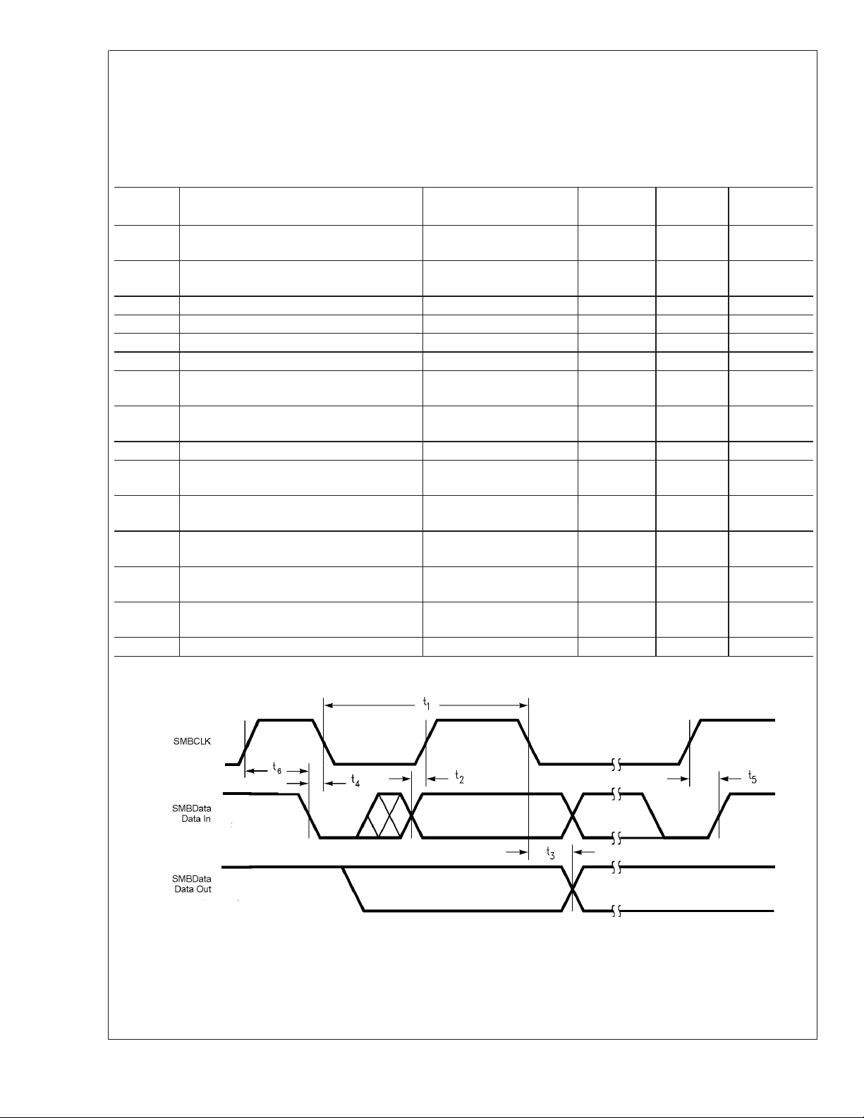
SMBus DIGITAL SWITCHING CHARACTERISTICS
Unless otherwise noted, these specifications apply for VCC=+3.0 Vdc to +3.6 Vdc, CL(load capacitance) on output lines = 80
pF. Boldface limits apply for T
A=TJ=TMIN
to T
characteristics of the LM82 fully meet or exceed the published specifications of the SMBus or I
eters are the timing relationships between SMBCLK and SMBData signals related to the LM82. They are not the I
bus specifications.
Symbol Parameter Conditions Typical Limits Units
f
SMB
t
LOW
t
LOW
t
HIGH
t
R,SMB
t
F,SMB
t
OF
t
TIMEOUT
SMBus Clock Frequency 100
SMBus Clock Low Time 10 % to 10 % 1.3
MEXT Cumulative Clock Low Extend Time 10 ms (max)
SMBus Clock High Time 90 % to 90% 0.6 µs (min)
SMBus Rise Time 10% to 90% 1 µs (max)
SMBus Fall Time 90% to 10% 0.3 ns (max)
Output Fall Time CL= 400 pF,
SMBData and SMBCLK Time Low for
Reset of Serial Interface (Note 12)
t
1
t
,
2
t
SU;DAT
,
t
3
t
HD;DAT
t4,
t
HD;STA
,
t
5
t
SU;STO
,
t
6
t
SU;STA
t
BUF
SMBCLK (Clock) Period 10 µs (min)
Data In Setup Time to SMBCLK High 100 ns (min)
Data Out Stable after SMBCLK Low 300
SMBData Low Setup Time to SMBCLK
Low
SMBData High Delay Time after SMBCLK
High (Stop Condition Setup)
SMBus Start-Condition Setup Time 0.6 µs (min)
SMBus Free Time 1.3 µs (min)
; all other limits TA=TJ= +25˚C, unless otherwise noted. The switching
MAX
2
C bus. The following param-
(Note 6) (Note 7) (Limit)
10
25
250 ns (max)
=3mA
I
O
25
40
TBD
100 ns (min)
100 ns (min)
2
C or SMBus
kHz (max)
kHz (min)
µs (min)
ms (max)
ms (min)
ms (max)
ns (min)
ns (max)
SMBus Communication
www.national.com 6
10129704
 Loading...