

查询LM13121Z-12供应商
LM320L/LM79LXXAC Series
3-Terminal Negative Regulators
General Description
The LM320L/LM79LXXAC dual marked series of 3-terminal
negative voltage regulators features fixed output voltages of
−5V, −12V, and −15V with output current capabilities in
excess of 100mA. These devices were designed using the
latest computer techniques for optimizing the packaged IC
thermal/electrical performance. The LM79LXXAC series,
even when combined with a minimum output compensation
capacitor of 0.1µF, exhibits an excellent transient response,
a maximum line regulation of 0.07% V
load regulation of 0.01% V
The LM320L/LM79LXXAC series also includes, as selfprotection circuitry: safe operating area circuitry for output
transistor power dissipation limiting, a temperature independent short circuit current limit for peak output current limiting,
and a thermal shutdown circuit to prevent excessive junction
temperature. Although designed primarily as fixed voltage
regulators, these devices may be combined with simple
external circuitry for boosted and/or adjustable voltages and
currents. The LM79LXXAC series is available in the 3-lead
O
/mA.
/V, and a maximum
O
February 2005
TO-92 package, 8-lead SOIC package, and the 6-Bump
micro SMD package. The LM320L series is available in the
3-lead TO-92 package.
For output voltage other than −5V, −12V and −15V, the
LM137L series provides an output voltage range from 1.2V
to 47V.
Features
n Preset output voltage error is less than±5% overload,
line and temperature
n Specified at an output current of 100mA
n Easily compensated with a small 0.1µF output
capacitor
n Internal short-circuit, thermal and safe operating area
protection
n Easily adjustable to higher output voltages
n Maximum line regulation less than 0.07% V
n Maximum load regulation less than 0.01% V
n See AN-1112 for micro SMD considerations
OUT
OUT
/V
/mA
LM320L/LM79LXXAC Series 3-Terminal Negative Regulators
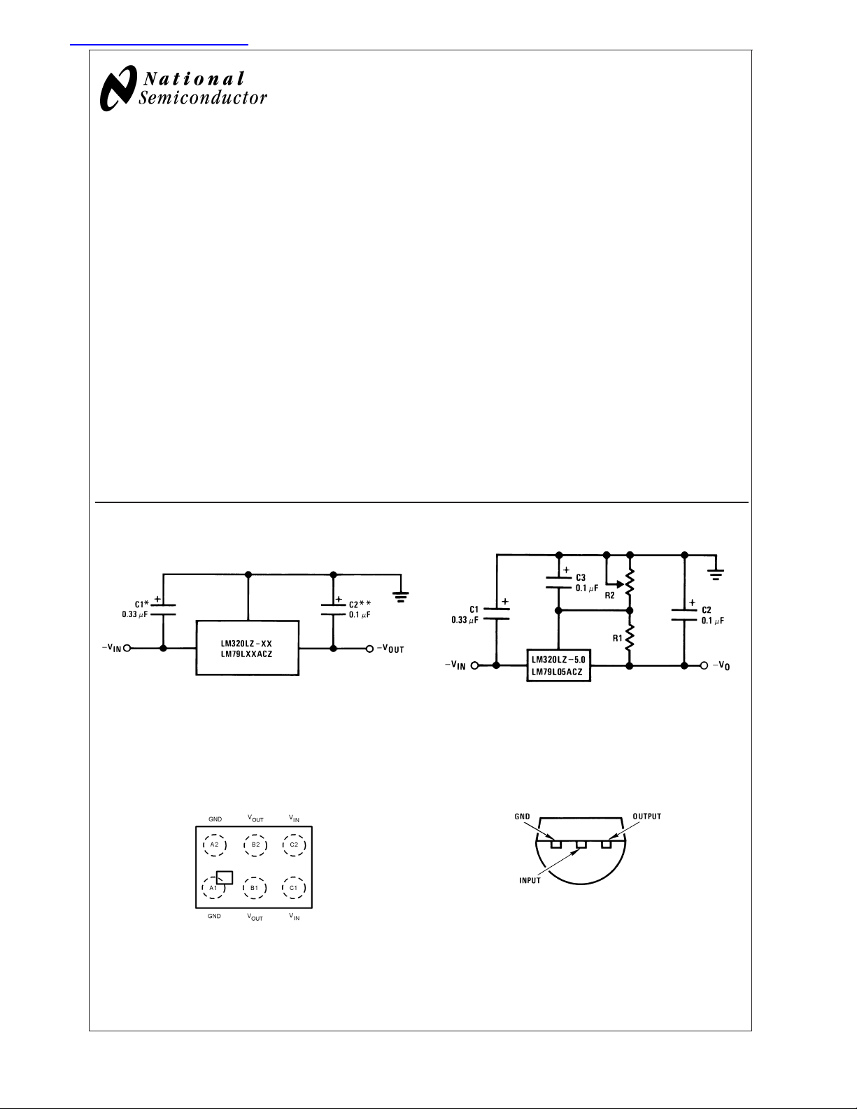
Typical Applications
Fixed Output Regulator
*Required if the regulator is located far from the power supply filter. A 1µF
aluminum electrolytic may be substituted.
*
*
Required for stability. A 1µF aluminum electrolytic may be substituted.
00774801
Connection Diagrams
6-Bump micro SMD
Bump Side Down
00774820
Adjustable Output Regulator
−V0= −5V − (5V/R1 + IQ)•R2,
>
3I
5V/R1
Q
TO-92 Plastic Package (Z)
Bottom View
00774803
00774802
© 2005 National Semiconductor Corporation DS007748 www.national.com
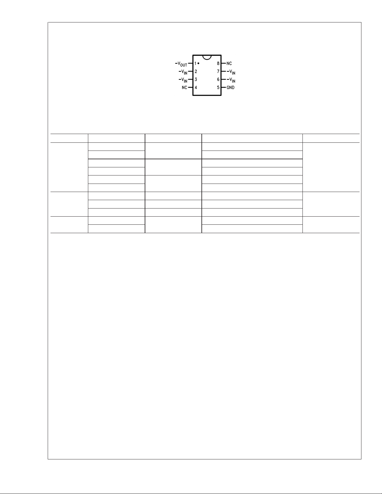
Connection Diagrams (Continued)
LM320L/LM79LXXAC
SO-8 Plastic (Narrow Body)
Top View
00774804
Ordering Information
Package Part Number Package Marking Transport Media NSC Drawing
8-Lead SOIC LM79L05ACM LM79L05ACM 95 Units/Rail M08A
LM79L05ACMX 2.5k Units Tape and Reel
LM79L13ACM LM79L12ACM 95 Units/Rail
LM79L13ACMX 2.5k Units Tape and Reel
LM79L15ACM LM79L15ACM 95 Units/Rail
LM79L15ACMX 2.5k Units Tape and Reel
3-Pin TO-92 LM79L05ACZ 320L79L05 1800 Units Per Box Z03A
LM79L12ACZ 320L79L12 1800 Units Per Box
LM79L15ACZ 320L79L15 1800 Units Per Box
6-Bump
micro SMD
LM79L15ACTL XTPB 250 Units Tape and Reel TLA06AMA
LM79L05ACTLX 3k Units Tape and Reel
www.national.com 2
LM320L/LM79LXXAC
Absolute Maximum Ratings (Note 1)
If Military/Aerospace specified devices are required,
please contact the National Semiconductor Sales Office/
Distributors for availability and specifications.
Input Voltage
= −5V, −12V, −15V −35V
V
O
Operating Temperature Range 0˚C to +70˚C
Maximum Junction Temperature +125˚C
Storage Temperature Range −55˚C to +150˚C
Lead Temperature
(Soldering, 10 sec.) 260˚C
Internal Power Dissipation (Note 2) Internally Limited
Electrical Characteristics (Note 3)
TA= 0˚C to +70˚C unless otherwise noted.
Output Voltage −5V −12V −15V
Input Voltage (unless otherwise noted) −10V −17V −20V Units
Symbol Parameter Conditions Min Typ Max Min Typ Max Min Typ Max
V
O
∆V
∆V
∆V
I
Q
∆I
Q
V
n
Note 1: Absolute Maximum Ratings indicate limits beyond which damage to the device may occur. Operating Ratings indicate conditions for which the device is
functional, but do not guarantee specific performance limits.
Note 2: Thermal resistance of Z package is 60˚C/W θ
maximum junction temperature shall not exceed 125˚C on electrical parameters.
Note 3: To ensure constant junction temperature, low duty cycle pulse testing is used.
Output
TJ= 25˚C, IO= 100mA −5.2 −5 −4.8 −12.5 −12 −11.5 −15.6 −15 −14.4
Voltage
1mA ≤ IO≤ 100mA −5.25 −4.75 −12.6 −11.4 −15.75 −14.25
V
≤ VIN≤ V
MIN
1mA ≤ I
V
≤ VIN≤ V
MIN
Line
O
TJ= 25˚C, IO= 100mA 60 45 45 mV
MAX
≤ 40mA −5.25 −4.75 −12.6 −11.4 −15.75 −14.25
O
MAX
(−20 ≤ VIN≤ −7.5) (−27 ≤ VIN≤ −14.8) (−30 ≤ VIN≤ −18) V
(−20 ≤ VIN≤ −7) (−27 ≤ VIN≤ −14.5) (−30 ≤ VIN≤ −17.5)
Regulation
O
Load
Regulation
≤ VIN≤ V
V
MIN
T
= 25˚C, IO= 40mA 60 45 45 mV
J
V
≤ VIN≤ V
MIN
MAX
MAX
TJ= 25˚C
(−20 ≤ VIN≤ −7.3) (−27 ≤ VIN≤ −14.6) (−30 ≤ VIN≤ −17.7) V
(−20 ≤ VIN≤ −7) (−27 ≤ VIN≤ −14.5) (−30 ≤ VIN≤ −17.5) V
50 100 125 mV
1mA ≤ IO≤ 100mA
O
Long Term
IO= 100mA 20 48 60 mV/khrs
Stability
Quiescent
IO= 100mA 2 6 2 6 2 6 mA
Current
Quiescent
1mA ≤ IO≤ 100mA 0.3 0.3 0.3
Current
Change 1mA ≤ IO≤ 40mA 0.1 0.1 0.1 mA
I
= 100mA 0.25 0.25 0.25 mA
O
V
Output Noise
Voltage
≤ VIN≤ V
MIN
MAX
TJ= 25˚C, IO= 100mA
(−20 ≤ VIN≤ −7.5) (−27 ≤ VIN≤ −14.8) (−30 ≤ VIN≤ −18) V
40 96 120 µV
f = 10Hz − 10kHz
Ripple
Rejection
Input Voltage T
Required to I
TJ= 25˚C, IO= 100mA
50 52 50 dB
f = 120Hz
= 25˚C, IO= 100mA −7.3 −14.6 −17.7 V
J
= 40mA −7.0 −14.5 −17.5 V
O
Maintain Line
Regulation
, 232˚C/W θJAat still air, and 88˚C/W at 400 ft/min of air. The M package θJAis 180˚C/W in still air. The
JC
www.national.com3
 Loading...