

LM78LXX Series
3-Terminal Positive Regulators
General Description
The LM78LXX series of three terminal positive regulators is
available with several fixed output voltages making them
useful in a wide range of applications. When used as a zener
diode/resistor combination replacement, the LM78LXX usually results in an effective output impedance improvement of
two orders of magnitude, and lower quiescent current. These
regulators can provide local on card regulation, eliminating
the distribution problems associated with single point regulation. The voltages available allow the LM78LXX to be used
in logic systems, instrumentation, HiFi, and other solid state
electronic equipment.
The LM78LXX is available in the plastic TO-92 (Z) package,
the plastic SO-8 (M) package and a chip sized package
(8-Bump micro SMD) using National’s micro SMD package
technology. With adequate heat sinking the regulator can
deliver 100mA output current. Current limiting is included to
limit the peak output current to a safe value. Safe area
protection for the output transistors is provided to limit inter-
nal power dissipation. If internal power dissipation becomes
too high for the heat sinking provided, the thermal shutdown
circuit takes over preventing the IC from overheating.
Features
n LM78L05 in micro SMD package
n Output voltage tolerances of
n Output current of 100mA
n Internal thermal overload protection
n Output transistor safe area protection
n Internal short circuit current limit
n Available in plastic TO-92 and plastic SO-8 low profile
n No external components
n Output voltages of 5.0V, 6.2V, 8.2V, 9.0V, 12V, 15V
n See AN-1112 for micro SMD considerations
range
packages
May 2003
±
5% over the temperature
LM78LXX Series 3-Terminal Positive Regulators
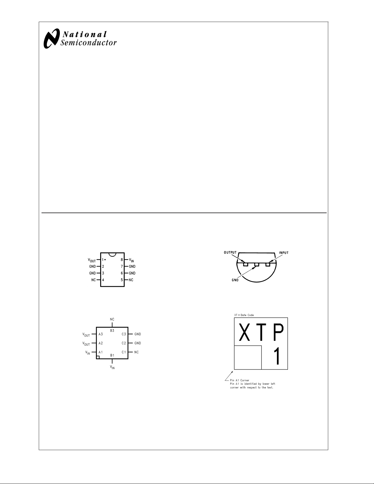
Connection Diagrams
SO-8 Plastic (M)
(Narrow Body)
Top View
8-Bump micro SMD
Top View
(Bump Side Down)
00774402
00774424
(TO-92)
Plastic Package (Z)
00774403
Bottom View
micro SMD Marking Orientation
00774433
Top View
© 2003 National Semiconductor Corporation DS007744 www.national.com
Absolute Maximum Ratings (Note 1)
If Military/Aerospace specified devices are required,
please contact the National Semiconductor Sales Office/
Distributors for availability and specifications.
Power Dissipation (Note 5) Internally Limited
LM78LXX Series
Input Voltage 35V
Storage Temperature −65˚C to +150˚C
ESD Susceptibility (Note 2) 1kV
Operating Junction Temperature
SO-8, TO-92 0˚C to 125˚C
micro SMD −40˚C to 85˚C
Soldering Information
Infrared or Convection (20 sec.) 235˚C
Wave Soldering (10 sec.) 260˚C (lead time)
LM78LXX Electrical Characteristics Limits in standard typeface are for T
= 25˚C, Bold typeface
J
applies over 0˚C to 125˚C for SO-8 and TO-92 packages, and −40˚C to 85˚C for micro SMD package. Limits are guaranteed by production testing or correlation techniques using standard Statistical Quality Control (SQC) methods. Unless otherwise specified: I
= 40mA, CI= 0.33µF, CO= 0.1µF.
O
LM78L05
Unless otherwise specified, VIN= 10V
Symbol Parameter Conditions Min Typ Max Units
∆V
∆V
I
Q
V
V
O
O
O
Q
n
Output Voltage 4.8 5 5.2
7V ≤ V
1mA ≤ I
IN
O
≤ 20V
≤ 40mA
4.75 5.25
(Note 3)
1mA ≤ I
(Note 3)
≤ 70mA
O
4.75 5.25
Line Regulation 7V ≤ VIN≤ 20V 18 75
8V ≤ V
≤ 20V 10 54
IN
Load Regulation 1mA ≤ IO≤ 100mA 20 60
1mA ≤ I
≤ 40mA 5 30
O
Quiescent Current 3 5
Quiescent Current Change 8V ≤ VIN≤ 20V 1.0
1mA ≤ I
Output Noise Voltage f = 10 Hz to 100 kHz
(Note 4)
≤ 40mA 0.1
O
40 µV
Ripple Rejection f = 120 Hz
8V ≤ V
IN
≤ 16V
47 62 dB
V
mV
mA∆I
I
PK
Peak Output Current 140 mA
Average Output Voltage Tempco IO= 5mA
−0.65 mV/˚C
V
(Min) Minimum Value of Input Voltage
IN
Required to Maintain Line Regulation
θ
JA
Thermal Resistance
(8-Bump micro SMD)
6.7 7 V
230.9 ˚C/W
LM78L62AC
Unless otherwise specified, VIN= 12V
Symbol Parameter Conditions Min Typ Max Units
V
O
www.national.com 2
Output Voltage 5.95 6.2 6.45
8.5V ≤ V
1mA ≤ I
≤ 20V
IN
≤ 40mA
O
5.9 6.5
(Note 3)
1mA ≤ I
(Note 3)
≤ 70mA
O
5.9 6.5
V
LM78LXX Series
LM78LXX Electrical Characteristics Limits in standard typeface are for T
= 25˚C, Bold typeface
J
applies over 0˚C to 125˚C for SO-8 and TO-92 packages, and −40˚C to 85˚C for micro SMD package. Limits are
guaranteed by production testing or correlation techniques using standard Statistical Quality Control (SQC) methods. Unless
otherwise specified: I
= 40mA, CI= 0.33µF, CO= 0.1µF. (Continued)
O
LM78L62AC (Continued)
Unless otherwise specified, VIN= 12V
Symbol Parameter Conditions Min Typ Max Units
∆V
O
∆V
O
I
Q
Q
V
n
I
PK
V
(Min) Minimum Value of Input Voltage
IN
Line Regulation 8.5V ≤ VIN≤ 20V 65 175
9V ≤ V
≤ 20V 55 125
IN
Load Regulation 1mA ≤ IO≤ 100mA 13 80
1mA ≤ I
≤ 40mA 6 40
O
Quiescent Current 2 5.5
Quiescent Current Change 8V ≤ VIN≤ 20V 1.5
1mA ≤ I
Output Noise Voltage f = 10 Hz to 100 kHz
(Note 4)
≤ 40mA 0.1
O
50 µV
Ripple Rejection f = 120 Hz
10V ≤ V
IN
≤ 20V
40 46 dB
Peak Output Current 140 mA
Average Output Voltage Tempco IO= 5mA
−0.75 mV/˚C
Required to Maintain Line Regulation
7.9 V
mV
mA∆I
LM78L82AC
Unless otherwise specified, VIN= 14V
Symbol Parameter Conditions Min Typ Max Units
V
∆V
∆V
I
Q
V
I
PK
O
O
O
Q
n
Output Voltage 7.87 8.2 8.53
11V ≤ V
1mA ≤ I
≤ 23V
IN
≤ 40mA
O
7.8 8.6
(Note 3)
1mA ≤ IO≤ 70mA
(Note 3)
7.8 8.6
Line Regulation 11V ≤ VIN≤ 23V 80 175
12V ≤ V
≤ 23V 70 125
IN
Load Regulation 1mA ≤ IO≤ 100mA 15 80
1mA ≤ I
≤ 40mA 8 40
O
Quiescent Current 2 5.5
Quiescent Current Change 12V ≤ VIN≤ 23V 1.5
1mA ≤ I
Output Noise Voltage f = 10 Hz to 100 kHz
(Note 4)
≤ 40mA 0.1
O
60 µV
Ripple Rejection f = 120 Hz
12V ≤ V
IN
≤ 22V
39 45 dB
Peak Output Current 140 mA
Average Output Voltage Tempco IO= 5mA
−0.8 mV/˚C
V
mV
mA∆I
V
(Min) Minimum Value of Input Voltage
IN
Required to Maintain Line Regulation
9.9 V
www.national.com3
LM78LXX Electrical Characteristics Limits in standard typeface are for T
= 25˚C, Bold typeface
J
applies over 0˚C to 125˚C for SO-8 and TO-92 packages, and −40˚C to 85˚C for micro SMD package. Limits are
guaranteed by production testing or correlation techniques using standard Statistical Quality Control (SQC) methods. Unless
otherwise specified: I
LM78L09AC
LM78LXX Series
Unless otherwise specified, VIN= 15V
= 40mA, CI= 0.33µF, CO= 0.1µF. (Continued)
O
Symbol Parameter Conditions Min Typ Max Units
V
O
Output Voltage 8.64 9.0 9.36
11.5V ≤ V
1mA ≤ I
IN
≤ 40mA
O
≤ 24V
8.55 9.45
(Note 3)
≤ 70mA
O
≤ 24V 90 150
IN
≤ 40mA 10 45
O
≤ 40mA 0.1
O
8.55 9.45
∆V
∆V
I
Q
V
1mA ≤ I
(Note 3)
O
Line Regulation 11.5V ≤ VIN≤ 24V 100 200
13V ≤ V
O
Load Regulation 1mA ≤ IO≤ 100mA 20 90
1mA ≤ I
Quiescent Current 2 5.5
Q
Quiescent Current Change 11.5V ≤ VIN≤ 24V 1.5
1mA ≤ I
n
Output Noise Voltage 70 µV
Ripple Rejection f = 120 Hz
15V ≤ V
IN
≤ 25V
38 44 dB
V
mV
mA∆I
I
PK
Peak Output Current 140 mA
Average Output Voltage Tempco IO= 5mA
−0.9 mV/˚C
V
(Min) Minimum Value of Input Voltage
IN
Required to Maintain Line Regulation
10.7 V
LM78L12AC
Unless otherwise specified, VIN= 19V
Symbol Parameter Conditions Min Typ Max Units
V
∆V
∆V
I
Q
V
O
O
O
Q
n
Output Voltage 11.5 12 12.5
14.5V ≤ V
1mA ≤ I
IN
≤ 40mA
O
≤ 27V
11.4 12.6
(Note 3)
1mA ≤ IO≤ 70mA
(Note 3)
11.4 12.6
Line Regulation 14.5V ≤ VIN≤ 27V 30 180
16V ≤ V
≤ 27V 20 110
IN
Load Regulation 1mA ≤ IO≤ 100mA 30 100
1mA ≤ I
≤ 40mA 10 50
O
Quiescent Current 3 5
Quiescent Current Change 16V ≤ VIN≤ 27V 1
1mA ≤ I
≤ 40mA 0.1
O
Output Noise Voltage 80 µV
Ripple Rejection f = 120 Hz
15V ≤ V
≤ 25
IN
40 54 dB
V
mV
mA∆I
I
PK
Peak Output Current 140 mA
Average Output Voltage Tempco IO= 5mA
www.national.com 4
−1.0 mV/˚C
 Loading...