

查询LM747供应商
LM747
Dual Operational Amplifier
LM747 Dual Operational Amplifier
November 1994
General Description
The LM747 is a general purpose dual operational amplifier.
The two amplifiers share a common bias network and power
supply leads. Otherwise, their operation is completely independent.
Additional features of the LM747 are: no latch-up when input common mode range is exceeded, freedom from oscillations, and package flexibility.
The LM747C/LM747E is identical to the LM747/LM747A
except that the LM747C/LM747E has its specifications
guaranteed over the temperature range from 0
instead of
b
55§Ctoa125§C.
Ctoa70§C
§
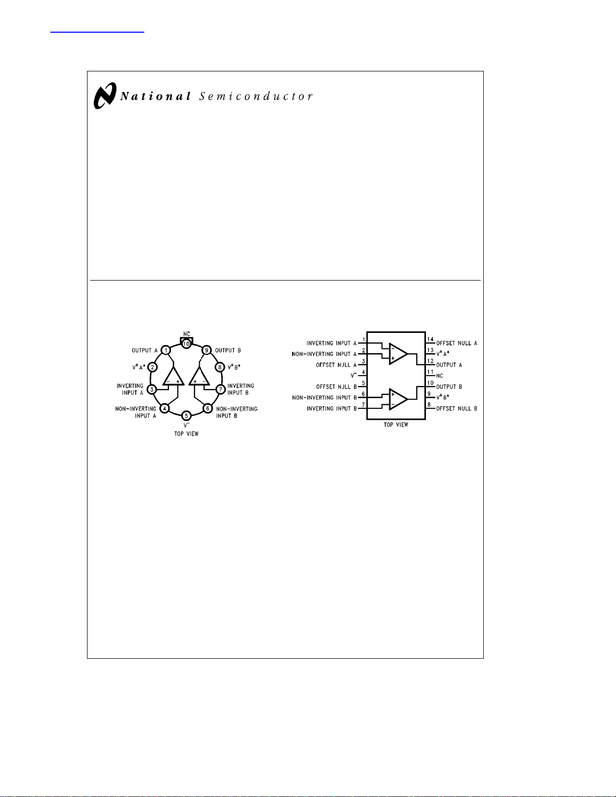
Connection Diagrams
Metal Can Package
TL/H/11479– 4
Order Number LM747H
See NS Package Number H10C
*VaA and VaB are internally connected.
Features
Y
No frequency compensation required
Y
Short-circuit protection
Y
Wide common-mode and differential voltage ranges
Y
Low power consumption
Y
No latch-up
Y
Balanced offset null
Dual-In-Line Package
Order Number LM747CN or LM747EN
See NS Package Number N14A
TL/H/11479– 5
C
1995 National Semiconductor Corporation RRD-B30M115/Printed in U. S. A.
TL/H/11479
Absolute Maximum Ratings
If Military/Aerospace specified devices are required,
please contact the National Semiconductor Sales
Office/Distributors for availability and specifications.
Supply Voltage
LM747/LM747A
LM747C/LM747E
g
22V
g
18V
Power Dissipation (Note 1) 800 mW
Differential Input Voltage
g
30V
Input Voltage (Note 2)
Output Short-Circuit Duration Indefinite
Operating Temperature Range
LM747/LM747A
LM747C/LM747E 0
Storage Temperature Range
Lead Temperature (Soldering, 10 sec.) 300§C
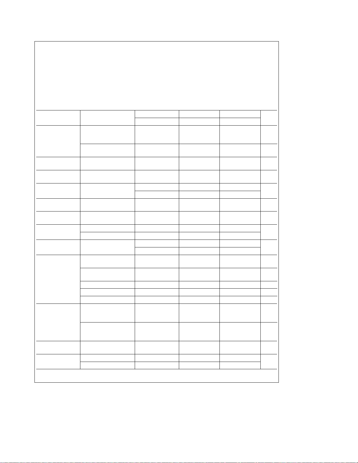
Electrical Characteristics (Note 3)
Parameter Conditions
Input Offset Voltage T
e
25§C
A
s
R
10 kX 1.0 5.0 2.0 6.0
S
s
R
50X 0.8 3.0
S
s
R
50X 4.0
S
s
R
10 kX 6.0 7.5
S
Average Input Offset 15
Voltage Drift
Input Offset Voltage T
Adjustment Range
Input Offset Current T
e
A
e
A
e
25§C, V
g
20V
S
25§C 3.0 30 20 200 20 200
Average Input Offset
Current Drift
Input Bias Current T
Input Resistance T
Input Voltage Range T
Large Signal T
Voltage Gain V
Output Voltage Swing V
Output Short T
Circuit Current 10 40
Common-Mode R
Rejection Ratio
e
25§C 30 80 80 500 80 500 nA
A
s
T
V
V
R
V
V
V
R
R
V
R
R
R
AMIN
A
S
A
A
S
S
L
S
S
S
S
L
L
S
L
L
A
S
S
s
T
T
A
AMAX
e
e
e
e
e
e
t
e
e
e
e
t
t
e
t
t
e
s
s
e
25§C, V
g
20V 0.5
g
20V 1.0 6.0 0.3 2.0 0.3 2.0
S
25§C
t
25§C, R
g
g
2kX
g
g
g
g
20V, V
15V, V
20V, V
15V, V
5V, V
20V
2kX
L
e
g
15V 50 V/mV
O
e
g
10V 50 200 20 200
O
e
g
15V 32 V/mV
O
e
g
10V 25 15 V/mV
O
e
g
2V 10 V/mV
O
10 kX
2kX
g
15V
10 kX
2kX
25§C1025352525
e
CM
CM
g
e
g
10 kX,V
50 kX,V
LM747A/LM747E LM747 LM747C
Min Typ Max Min Typ Max Min Typ Max
g
10
0.5 nA/
0.210 1.5 0.8 mA
g12g
g
g
13
16
15
12V 70 90 70 90
12V 80 95
b
55§Ctoa125§C
Ctoa70§C
§
b
65§Ctoa150§C
g
15
g
15 mV
70 85 500 300
g12g
13
g12g
13
g12g
g10g
14
13
g12g
g10g
14
13
g
Units
mV/
V/mV
15V
mV
mV
nA
MX
mA
dB
C
§
C
§
V
V
V
2
Electrical Characteristics (Note 3) (Continued)
Parameter Conditions
e
Supply Voltage V
Rejection Ratio R
Transient Response T
Rise Time 0.25 0.8 0.3 0.3 ms
g
20V to V
S
s
50X 86 96
S
s
10 kX 77 96 77 96
R
S
e
25§C, Unity Gain
A
e
g
S
Overshoot 6.0 20 5 5 %
Bandwidth (Note 4) T
Slew Rate T
Supply Current/Amp T
Power Consumption/Amp T
LM747A V
LM747E V
LM747 V
Note 1: The maximum junction temperature of the LM747C/LM747E is 100§C. For operating at elevated temperatures, devies in the TO-5 package must be
derated based on a thermal resistance of 150
W, junction to ambient.
Note 2: For supply voltages less than
Note 3: These specifications apply for
specified. The LM747 and LM747C are specified for V
Note 4: Calculated value from: 0.35/Rise Time (m s).
e
25§C 0.437 1.5 MHz
A
e
25§C, Unity Gain 0.3 0.7 0.5 0.5 V/ms
A
e
25§C 2.5 1.7 2.8 1.7 2.8 mA
A
e
25§C
A
e
g
20V 80 150
V
S
e
g
V
15V 50 85 50 85
S
e
g
20V
S
e
T
T
A
AMIN
e
T
T
A
AMAX
e
g
20V 150
S
e
T
T
A
AMIN
e
T
T
A
AMAX
e
g
15V
S
e
T
T
A
AMIN
e
T
T
A
AMAX
C/W, junction to ambient, or 45§C/W, junction to case. The thermal resistance of the dual-in-line package is 100§C/
§
g
15V, the absolute maximum input voltage is equal to the supply voltage.
s
g
5VsV
g
20V andb55§CsT
S
e
S
LM747A/LM747E LM747 LM747C
Min Typ Max Min Typ Max Min Typ Max
5V
165
135
150 mW
150
60 100
45 75
g
15V andb55§CsT
s
125§C for the LM747A and 0§CsT
A
s
125§C and 0§CsT
A
s
70§C for the LM747E unless otherwise
A
s
70§C, respectively, unless otherwise specified.
A
Units
dB
mW
mW
mW
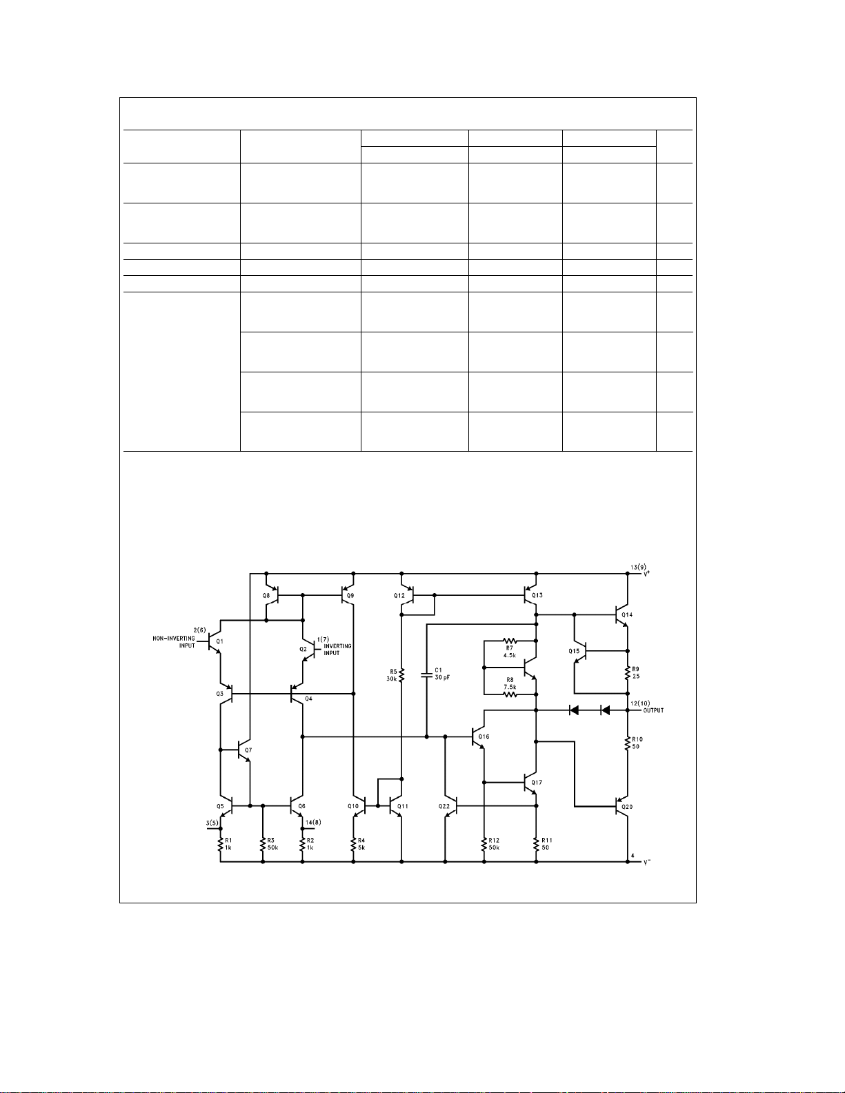
Schematic Diagram (Each Amplifier)
Note: Numbers in parentheses are pin numbers for amplifier B. DIP only.
TL/H/11479– 1
3
 Loading...