

查询LM741AH/883供应商
LM741
Operational Amplifier
General Description
The LM741 series are general purpose operational amplifiers which feature improved performance over industry standards like the LM709. They are direct, plug-in replacements
for the 709C, LM201, MC1439 and 748 in most applications.
The amplifiers offer many features which make their application nearly foolproof: overload protection on the input and
output, no latch-up when the common mode range is exceeded, as well as freedom from oscillations.
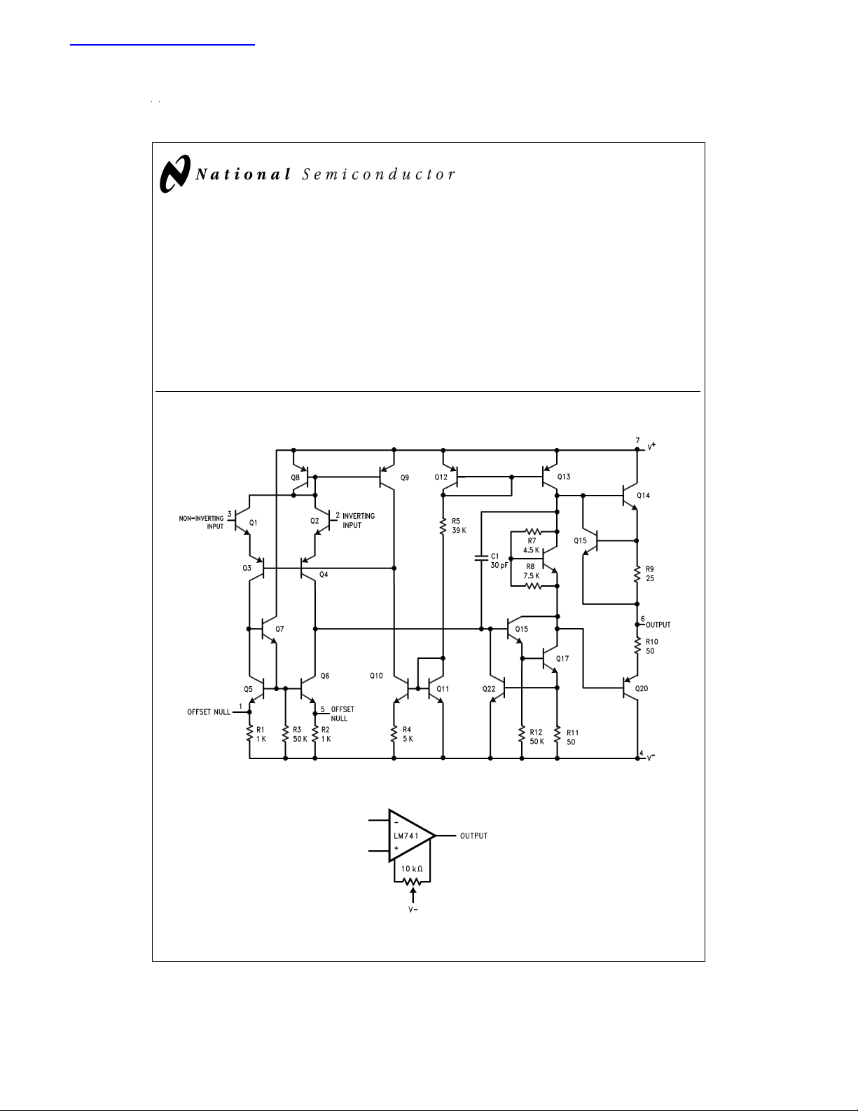
Schematic Diagram
LM741 Operational Amplifier
May 1998
The LM741C/LM741E are identical to the LM741/LM741A
except that the LM741C/LM741E have their performance
guaranteed over a 0˚C to +70˚C temperature range, instead
of −55˚C to +125˚C.
DS009341-1
Offset Nulling Circuit
DS009341-7
© 1999 National Semiconductor Corporation DS009341 www.national.com

Absolute Maximum Ratings (Note 1)
If Military/Aerospace specified devices are required, please contact the National Semiconductor Sales Office/
Distributors for availability and specifications.
(Note 6)
LM741A LM741E LM741 LM741C
Supply Voltage
±
22V
±
22V
±
22V
±
18V
Power Dissipation (Note 2) 500 mW 500 mW 500 mW 500 mW
Differential Input Voltage
Input Voltage (Note 3)
±
30V
±
15V
±
30V
±
15V
±
30V
±
15V
±
30V
±
15V
Output Short Circuit Duration Continuous Continuous Continuous Continuous
Operating Temperature Range −55˚C to +125˚C 0˚C to +70˚C −55˚C to +125˚C 0˚C to +70˚C
Storage Temperature Range −65˚C to +150˚C −65˚C to +150˚C −65˚C to +150˚C −65˚C to +150˚C
Junction Temperature 150˚C 100˚C 150˚C 100˚C
Soldering Information
N-Package (10 seconds) 260˚C 260˚C 260˚C 260˚C
J- or H-Package (10 seconds) 300˚C 300˚C 300˚C 300˚C
M-Package
Vapor Phase (60 seconds) 215˚C 215˚C 215˚C 215˚C
Infrared (15 seconds) 215˚C 215˚C 215˚C 215˚C
See AN-450 “Surface Mounting Methods and Their Effect on Product Reliability” for other methods of soldering
surface mount devices.
ESD Tolerance (Note 7) 400V 400V 400V 400V
Electrical Characteristics (Note 4)
Parameter Conditions LM741A/LM741E LM741 LM741C Units
Min Typ Max Min Typ Max Min Typ Max
Input Offset Voltage T
Average Input Offset 15 µV/˚C
Voltage Drift
Input Offset Voltage T
Adjustment Range
Input Offset Current T
Average Input Offset 0.5 nA/˚C
Current Drift
Input Bias Current T
Input Resistance T
Input Voltage Range T
=
25˚C
A
R
≤ 10 kΩ 1.0 5.0 2.0 6.0 mV
S
R
≤ 50Ω 0.8 3.0 mV
S
T
≤ TA≤ T
AMIN
AMAX
RS≤ 50Ω 4.0 mV
R
≤ 10 kΩ 6.0 7.5 mV
S
=
A
=
A
T
AMIN
=
A
T
AMIN
=
A
T
AMIN
=
V
S
=
A
T
AMIN
=
25˚C, V
±
20V
S
±
10
±
15
±
15 mV
25˚C 3.0 30 20 200 20 200 nA
≤ TA≤ T
AMAX
70 85 500 300 nA
25˚C 30 80 80 500 80 500 nA
≤ TA≤ T
25˚C, V
≤ TA≤ T
±
20V
25˚C
≤ TA≤ T
AMAX
=
±
20V 1.0 6.0 0.3 2.0 0.3 2.0 MΩ
S
, 0.5 MΩ
AMAX
AMAX
0.210 1.5 0.8 µA
±12±
13 V
±12±
13 V
www.national.com 2
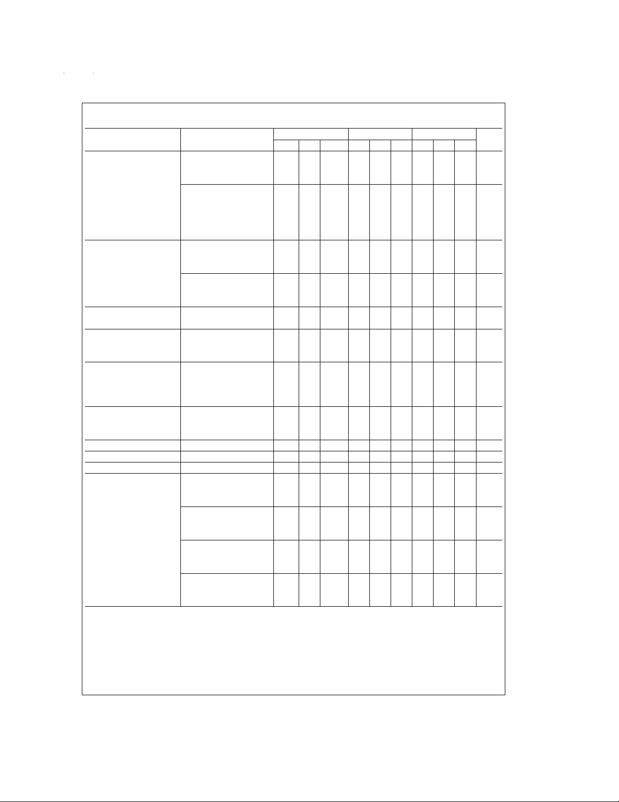
Electrical Characteristics (Note 4) (Continued)
Parameter Conditions LM741A/LM741E LM741 LM741C Units
Min Typ Max Min Typ Max Min Typ Max
Large Signal Voltage Gain T
Output Voltage Swing V
Output Short Circuit T
Current T
Common-Mode T
Rejection Ratio RS≤ 10 kΩ,V
Supply Voltage Rejection T
Ratio V
Transient Response T
Rise Time 0.25 0.8 0.3 0.3 µs
Overshoot 6.0 20 5 5
Bandwidth (Note 5) T
Slew Rate T
Supply Current T
Power Consumption T
LM741A V
LM741E V
LM741 V
Note 1: “Absolute Maximum Ratings” indicate limits beyond which damage to the device may occur. Operating Ratings indicate conditions for which the device is
functional, but do not guarantee specific performance limits.
=
A
=
V
S
=
V
S
T
AMIN
R
≥ 2kΩ,
L
=
V
S
=
V
S
=
V
S
=
S
R
≥ 10 kΩ
L
R
≥ 2kΩ
L
=
V
S
R
≥ 10 kΩ
L
R
≥ 2kΩ
L
=
A
AMIN
AMIN
R
≤ 50Ω,V
S
AMIN
=
S
R
≤ 50Ω 86 96 dB
S
R
≤ 10 kΩ 77 96 77 96 dB
S
=
A
=
A
=
A
=
A
=
A
=
V
S
=
V
S
=
S
=
T
A
=
T
A
=
S
=
T
A
=
T
A
=
S
=
T
A
=
T
A
≥ 2kΩ
25˚C, R
L
20V, V
15V, V
20V, V
15V, V
5V, V
20V
15V
=
±
15V 50 V/mV
O
=
±
10V 50 200 20 200 V/mV
O
,
AMAX
=
±
15V 32 V/mV
O
=
±
10V 25 15 V/mV
O
=
±
2V 10 V/mV
O
±
16 V
±
15 V
±12±
±10±
14
13
±12±
±10±
14 V
13 V
±
±
≤ TA≤ T
±
±
±
±
±
25˚C 10 25 35 25 25 mA
≤ TA≤ T
≤ TA≤ T
≤ TA≤ T
±
20V to V
AMAX
AMAX
=
±
CM
=
±
12V 80 95 dB
CM
,
AMAX
=
±
S
10 40 mA
12V 70 90 70 90 dB
5V
25˚C, Unity Gain
25˚C 0.437 1.5 MHz
25˚C, Unity Gain 0.3 0.7 0.5 0.5 V/µs
25˚C 1.7 2.8 1.7 2.8 mA
25˚C
±
20V 80 150 mW
±
15V 50 85 50 85 mW
±
20V
T
T
±
T
T
±
T
T
AMIN
AMAX
20V
AMIN
AMAX
15V
AMIN
AMAX
165 mW
135 mW
150 mW
150 mW
60 100 mW
45 75 mW
%
www.national.com3
 Loading...