

查询LM74供应商
LM74
LM74 SPI/MICROWIRE 12-Bit Plus Sign Temperature Sensor
April 2003
SPI/MICROWIRE
™
12-Bit Plus Sign Temperature Sensor
General Description
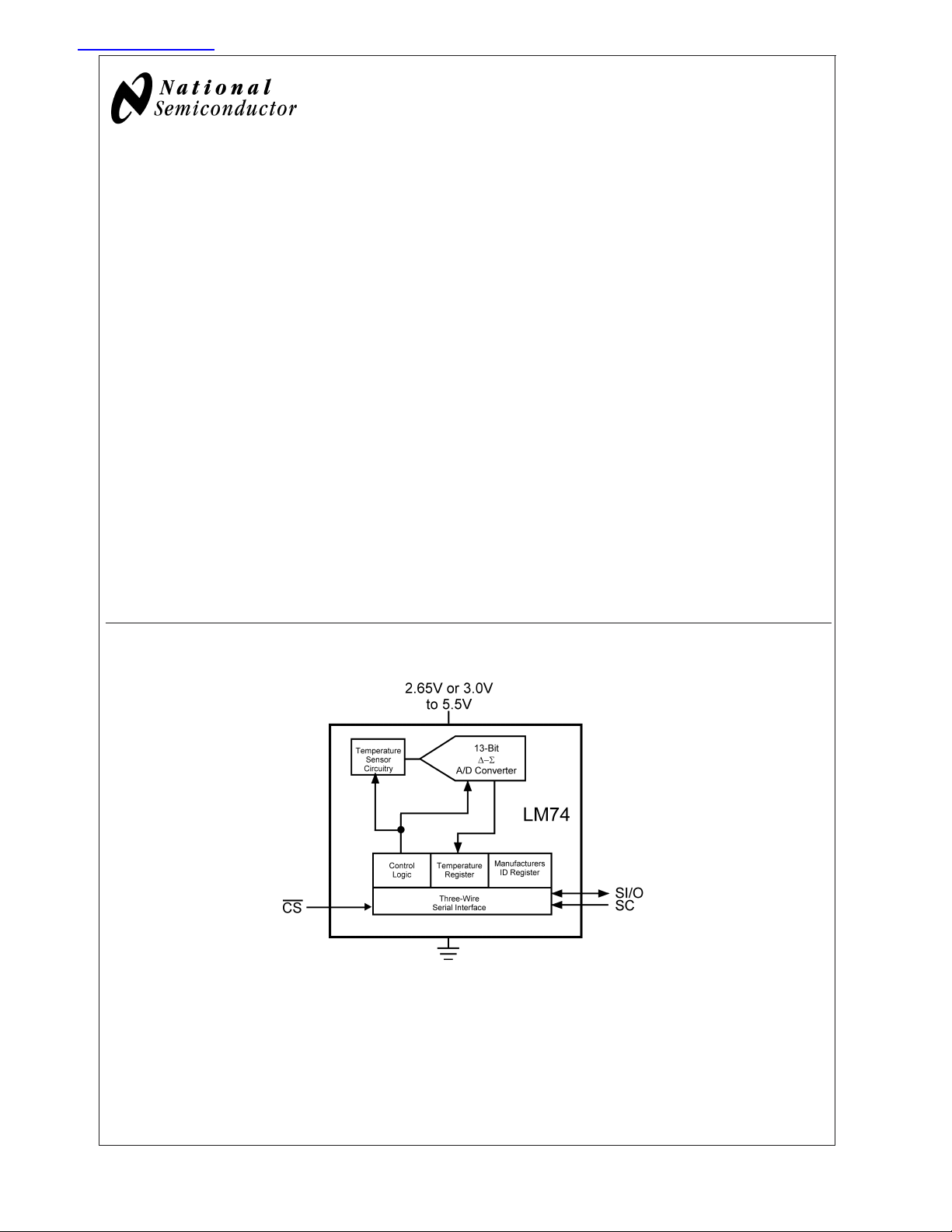
The LM74 is a temperature sensor, Delta-Sigma analog-todigital converter with an SPI and MICROWIRE compatible
interface. The host can query the LM74 at any time to read
temperature. A shutdown mode decreases power consumption to less than 10 µA. This mode is useful in systems where
low average power consumption is critical.
The LM74 has 12-bit plus sign temperature resolution
(0.0625˚C per LSB) while operating over a temperature
range of −55˚C to +150˚C.
The LM74’s 3.0V to 5.5V supply voltage range, low supply
current and simple SPI interface make it ideal for a wide
range of applications. These include thermal management
and protection applications in hard disk drives, printers, electronic test equipment, and office electronics. The LM74 is
available in the SO-8 package as well as an 5-Bump micro
SMD package.
Applications
n System Thermal Management
n Personal Computers
n Disk Drives
n Office Electronics
n Electronic Test Equipment
Features
n 0.0625˚C temperature resolution.
n Shutdown mode conserves power between temperature
reading
n SPI and MICROWIRE Bus interface
n 5-Bump micro SMD package saves space
Key Specifications
j
Supply Voltage 3.0V or 2.65V to
5.5V
j
Supply Current operating 265µA (typ)
520µA (max)
shutdown 3µA (typ)
j
Temperature
±
Accuracy −10˚C to 65˚C
−25˚C to 110˚C
−55˚C to 125˚C
1.25˚C(max)
±
2.1˚C(max)
±
3˚C(max)
Simplified Block Diagram
10090901
MICROWIRE®is a registered trademark of National Semiconductor Corporation.
®
TRI-STATE
© 2003 National Semiconductor Corporation DS100909 www.national.com
is a registered trademark of National Semiconductor Corporation.
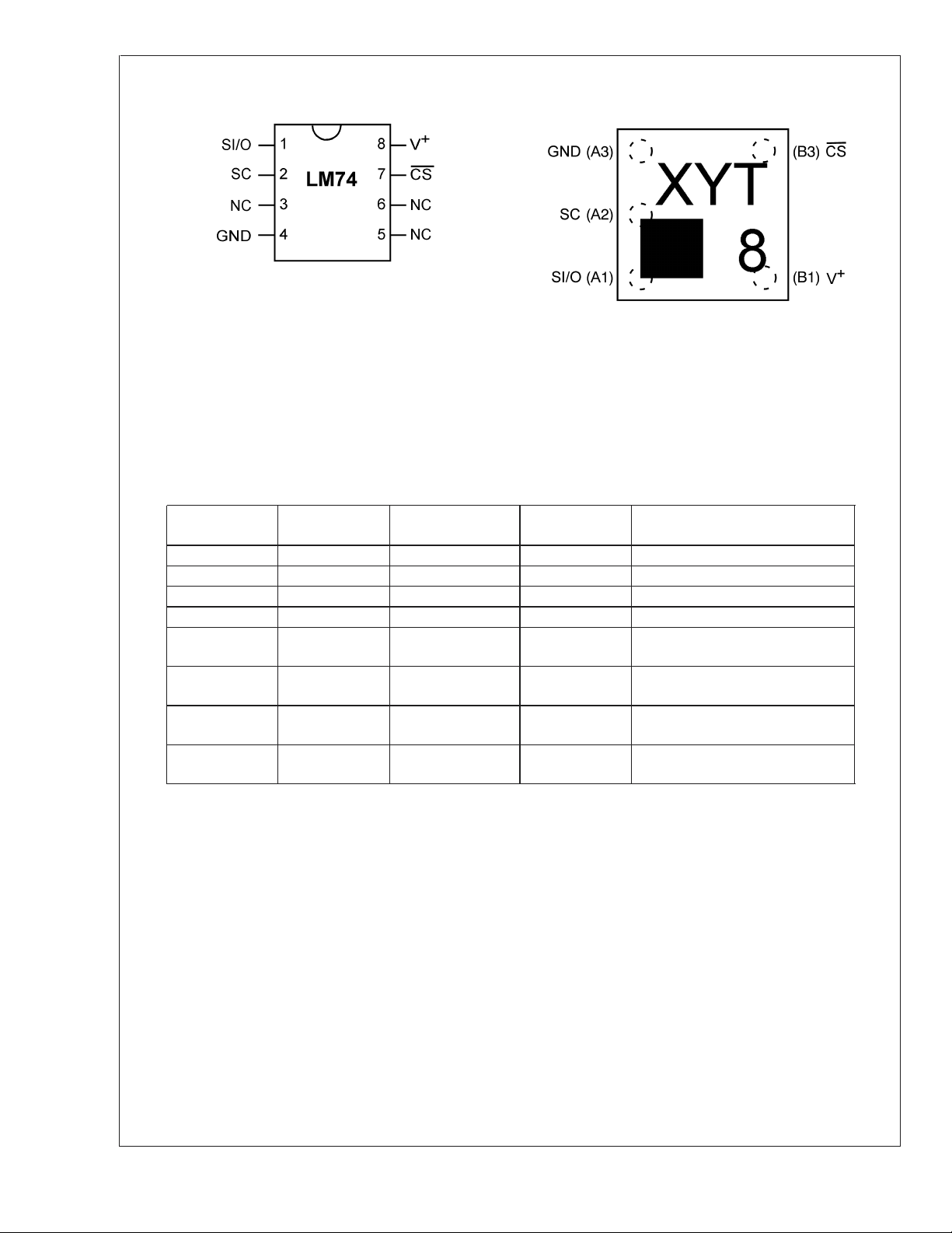
Connection Diagrams
LM74
SO-8 5-Bump micro SMD
TOP VIEW
10090902
NS Package Number M08A
Note:
- Pin numbers are referenced to the package marking text orientation. Pin
1 is designated by the square.
- Reference JEDEC Registration MO-211, variation BC
- The top 4 characters designate the date code. The bottom 3 characters
designate the device type (see ordering information).
TOP VIEW
NS Package Number BPD05MPB
Ordering Information
Order Number
Package
Marking
LM74CIM-3 LM74CIM-3 SO-8, M08A 3.0V to 3.6V 95 Units in Rail
LM74CIMX-3 LM74CIM-3 SO-8, M08A 3.0V to 3.6V 2500 Units in Tape and Reel
LM74CIM-5 LM74CIM-5 SO-8, M08A 4.5V to 5.5V 95 Units in Rail
LM74CIMX-5 LM74CIM-5 SO-8, M08A 4.5V to 5.5V 2500 Units in Tape and Reel
LM74CIBP-3 T8 micro SMD,
LM74CIBPX-3 T8 micro SMD,
LM74CIBP-5 T9 micro SMD,
LM74CIBPX-5 T9 micro SMD,
NS Package
Number
BPD05MPB
BPD05MPB
BPD05MPB
BPD05MPB
Supply Voltage Transport Media
2.65V to 3.6V 250 Units in Tape and Reel
2.65V to 3.6V 3000 Units in Tape and Reel
4.5V to 5.5V 250 Units in Tape and Reel
4.5V to 5.5V 3000 Units in Tape and Reel
10090924
www.national.com 2
Pin Descriptions
LM74
Label SO-8
Pin
SI/O 1 1 Slave Input/Output - Serial bus bi-directional data
SC 2 5 Slave Clock - Serial bus clock Schmitt trigger input
NC 3 No Connection No Connection
GND 4 4 Power Supply Ground Ground
NC 5 No Connection No Connection
NC 6 No Connection No Connection
CS
+
V
micro
#
SMD
#
Pin
line. Schmitt trigger input.
line.
7 3 Chip Select input. From Controller
8 2 Positive Supply Voltage Input DC Voltage from 3.0V to 5.5V for the
Function Typical Connection
From and to Controller
From Controller
LM74CIM and 2.65V to 5.5V for the
LM74CIBP. Bypass with a 0.1 µF ceramic
capacitor.
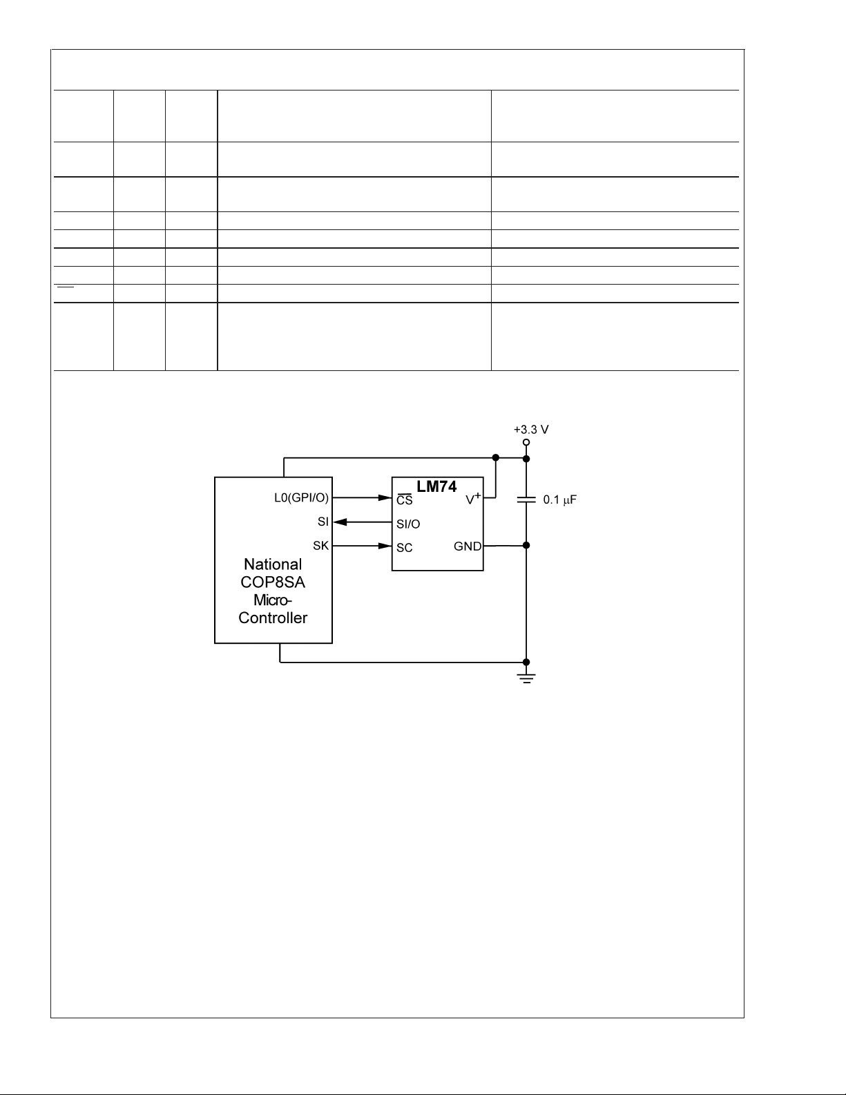
Typical Application
FIGURE 1. COP Microcontroller Interface
10090903
www.national.com3
Absolute Maximum Ratings (Note 1)
LM74
Supply Voltage −0.3V to 6.0V
Voltage at any Pin −0.3V to V
+
+ 0.3V
LM74CIM and LM74CIBP all
other pins
Machine Model 200V
Input Current at any Pin (Note 2) 5 mA
Package Input Current (Note 2) 20 mA
Storage Temperature −65˚C to +150˚C
Soldering Information, Lead Temperature
SO-8 Package (Note 3)
Vapor Phase (60 seconds)
Infrared (15 seconds)
215˚C
220˚C
ESD Susceptibility (Note 4)
Human Body Mode
Operating Ratings
Specified Temperature Range T
(Note 5)
LM74CIBP
LM74CIM
Supply Voltage Range (+V
)
S
LM74CIBP +2.65V to +5.5V
LM74CIM +3.0V to +5.5V
MIN
−40˚C to +125˚C
−55˚C to +150˚C
LM74CIBP SC, pin 5 1900V
Temperature-to-Digital Converter Characteristics
Unless otherwise noted, these specifications apply for V+= 2.65V to 3.6V for the LM74CIBP -3, V+= 3.0V to 3.6V for the
LM74CIM -3 and V
its T
=+25˚C, unless otherwise noted.
A=TJ
Temperature Error (Note 6) T
Resolution 13 Bits
Temperature
Conversion Time
Quiescent Current SO-8 Serial Bus Inactive 310 520 520 µA (max)
+
= 4.5V to 5.5V for the LM74 -5 (Note 6). Boldface limits apply for TA=TJ=T
Parameter Conditions
= −10˚C to +65˚C
A
T
= −25˚C to +110˚C
A
T
= −40˚C to +85˚C +2.65/−1.65
A
T
= −40˚C to +110˚C +2.65/
A
= −55˚C to +125˚C
T
A
T
= −55˚C to +150˚C
A
SO-8 (Note 9) 280 425 425 ms (max)
micro SMD (Note 9) 611 925 925 ms (max)
micro SMD 265 470 470 µA (max)
SO-8 Serial Bus Active 310 µA
micro SMD 310 µA
SO-8 Shutdown Mode,
+
V
micro SMD 3 µA
= 3.3V
SO-8 Shutdown Mode,
+
V
micro SMD 4 µA
=5V
Typical
(Note 7)
to T
MIN
LM74-5
Limits
(Note 8)
±
1.25
±
2.1 +2.65/−2.15 ˚C (max)
LM74-3
Limits
(Note 8)
±
1.25 ˚C (max)
±
2.15 ˚C (max)
; all other lim-
MAX
+2.65/−2.15 ˚C (max)
−2.0
±
3.0
±
5.0
±
3.5 ˚C (max)
±
5.0 ˚C (max)
7µA
8µA
2000V
to T
Units
(Limit)
MAX
Logic Electrical Characteristics
DIGITAL DC CHARACTERISTICS Unless otherwise noted, these specifications apply for V+= 2.65V to 3.6V for the
LM74CIBP -3, V
for T
A=TJ=TMIN
Symbol Parameter Conditions
V
IN(1)
V
IN(0)
I
IN(1)
www.national.com 4
+
= 3.0V to 3.6V for the LM74CIM -3 and V+= 4.5V to 5.5V for the LM74 -5 (Note 6). Boldface limits apply
to T
; all other limits TA=TJ=+25˚C, unless otherwise noted.
MAX
Typical
(Note 7)
Limits
(Note 8)
Logical “1” Input Voltage V+x 0.7 V (min)
+
V
+ 0.3 V (max)
Logical “0” Input Voltage −0.3 V (min)
+
V
Input Hysteresis Voltage V
+
= 3.0V to 3.6V 0.8 0.35 V (min)
+
V
= 4.5V to 5.5V 0.8 0.33 V (min)
Logical “1” Input Current VIN=V
+
0.005 3.0 µA (max)
x 0.3 V (max)
Units
(Limit)
Logic Electrical Characteristics (Continued)
DIGITAL DC CHARACTERISTICS Unless otherwise noted, these specifications apply for V+= 2.65V to 3.6V for the
LM74CIBP -3, V
for T
A=TJ=TMIN
Symbol Parameter Conditions
I
IN(0)
C
IN
V
OH
V
OL
I
O_TRI-STATE
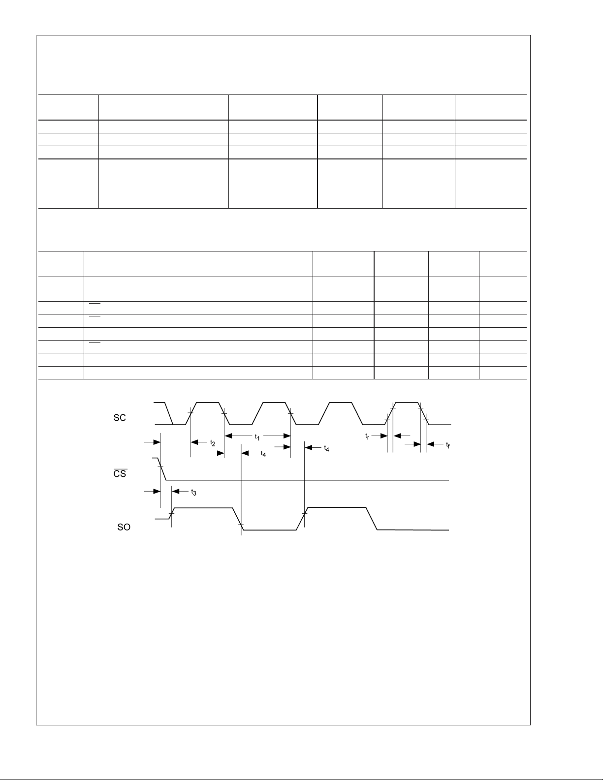
SERIAL BUS DIGITAL SWITCHING CHARACTERISTICS Unless otherwise noted, these specifications apply for V+= 2.65V
to 3.6V for the LM74CIBP -3, V
capacitance) on output lines = 100 pF unless otherwise specified. Boldface limits apply for T
limits T
A=TJ
Symbol Parameter Conditions
t
1
t
2
t
3
t
4
t
5
t
6
t
7
+
= 3.0V to 3.6V for the LM74CIM -3 and V+= 4.5V to 5.5V for the LM74 -5 (Note 6). Boldface limits apply
to T
; all other limits TA=TJ=+25˚C, unless otherwise noted.
MAX
Typical
(Note 7)
Limits
(Note 8)
Units
(Limit)
Logical “0” Input Current VIN= 0V −0.005 −3.0 µA (min)
All Digital Inputs 20 pF
High Level Output Voltage IOH= −400 µA 2.4 V (min)
Low Level Output Voltage IOL=+2mA 0.4 V (max)
TRI-STATE Output Leakage
Current
VO= GND
+
=V
V
O
−1
+1
µA (min)
µA
(max)
+
= 3.0V to 3.6V for the LM74CIM -3 and V+= 4.5V to 5.5V for the LM74 -5 (Note 6); CL(load
A=TJ=TMIN
to T
MAX
; all other
= +25˚C, unless otherwise noted.
Typical
(Note 7)
SC (Clock) Period 0.16
Limits
(Note 8)
DC
Units
(Limit)
µs (min)
(max)
CS Low to SC (Clock) High Set-Up Time 100 ns (min)
CS Low to Data Out (SO) Delay 70 ns (max)
SC (Clock) Low to Data Out (SO) Delay 100 ns (max)
CS High to Data Out (SO) TRI-STATE 200 ns (max)
SC (Clock) High to Data In (SI) Hold Time 50 ns (min)
Data In (SI) Set-Up Time to SC (Clock) High 30 ns (min)
LM74
FIGURE 2. Data Output Timing Diagram
10090904
www.national.com5
 Loading...