

National Semiconductor LM7372 Technical data
查询L7372供应商
LM7372
High Speed, High Output Current, Dual Operational
Amplifier
LM7372 High Speed, High Output Current, Dual Operational Amplifier
February 2002
General Description
The LM7372 is a high speed dual voltage feedback amplifier
that has the slewing characteristic of current feedback amplifiers; yet it can be used in all traditional voltage feedback
amplifier configurations.
The LM7372 is stable for gains as low as +2 or −1. It
provides a very high slew rate at 3000V/µs and a wide gain
bandwidth product of 120MHz, while consuming only
6.5mA/per amplifier ofsupplycurrent. It is ideal for video and
high speed signal processing applications such as xDSL and
pulse amplifiers. With 150mA output current, the LM7372
can be used for video distribution, as a transformer driver or
as a laser diode driver.
Operation on
swings and provides greater dynamic range and
signal-to-noise ratio. The LM7372 offers high SFDR and low
THD, ideal for ADC/DAC systems. In addition, the LM7372 is
specified for
The LM7372 is built on National’s Advance VIP
cally integrated PNP) complementary bipolar process.
±
15V power supplies allows for large signal
±
5V operation for portable applications.
™
III (Verti-
Typical Application
Features
n −80dBc highest harmonic distortion@1MHz, 2V
n Very high slew rate: 3000V/µs
n Wide gain bandwidth product: 120MHz
n −3dB frequency
n Low supply current: 13mA (both amplifiers)
n High open loop gain: 85dB
n High output current: 150mA
n Differential gain and phase: 0.01%, 0.02˚
@
AV= +2: 200MHz
Applications
n HDSL and ADSL Drivers
n Multimedia broadcast systems
n Professional video cameras
n CATV/Fiber optics signal processing
n Pulse amplifiers and peak detectors
n HDTV amplifiers
PP
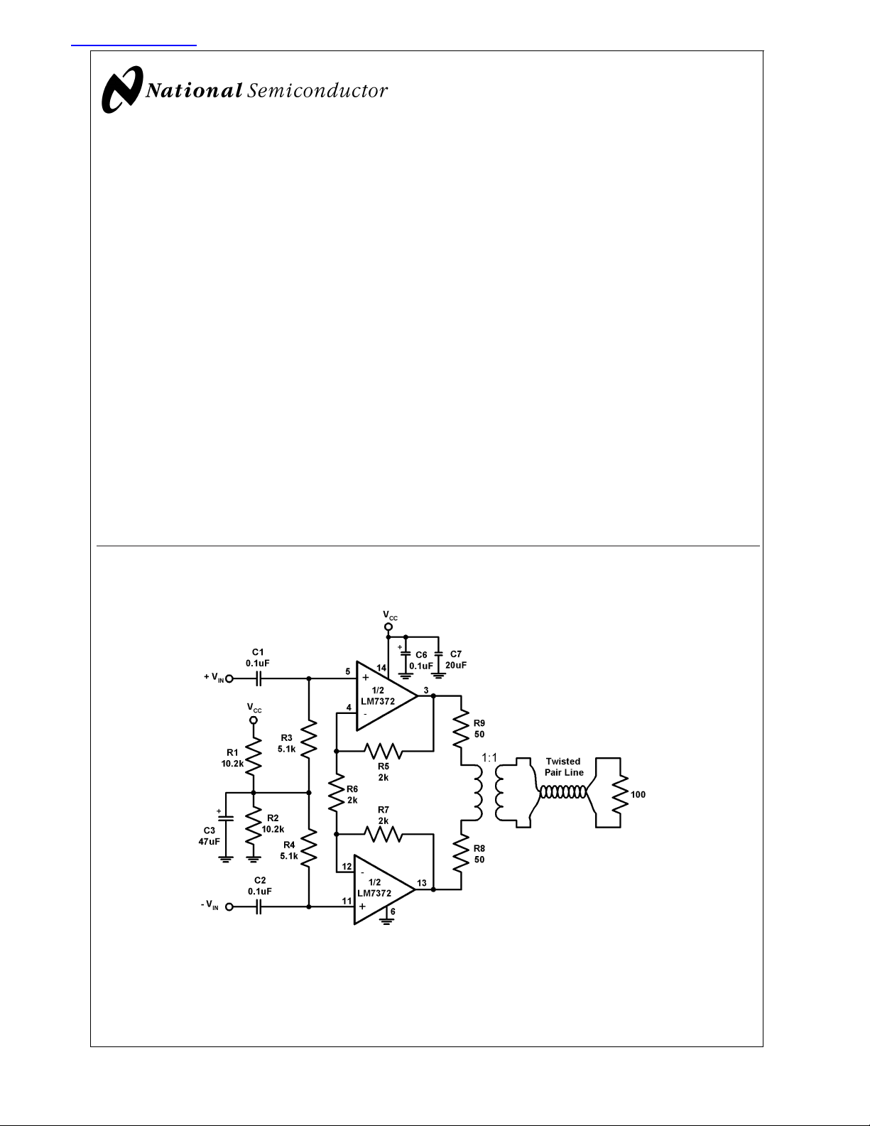
20004903
FIGURE 1. Single Supply Application (SOIC-16)
© 2002 National Semiconductor Corporation DS200049 www.national.com
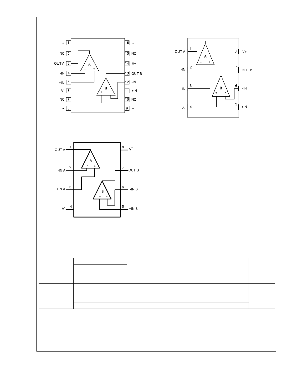
Connection Diagrams
LM7372
16-Pin SOIC 8-Contact LLP
20004902
20004901
Top View
*
Heatsink Pins. See note 4
Top View
8-Pin PSOP
Top View
20004929
For PSOP SOIC-8 the exposed pad should be tied either to V−or left
electrically floating. (die attach material is conductive and is internally
−
)
tied to V
Ordering Information
Symbol Temperature Range Package Markiing Transport Media NSC
−40˚C to +85˚C
16-Pin SOIC
8-Pin LLP
8-Pin PSOP
LM7372IMA LM7372IMA Rails
LM7372IMAX LM7372IMA 2.5k Units Tape and Reel
LM7372ILD L7372 1k Units Tape and Reel
LM7372ILDX L7372 4.5k Units Tape and Reel
LM7372MR LM7372MR Rails
LM7372MRX LM7372MR 2.5k Units Tape and Reel
Drawing
M16A
LDC08A
MRA08A
www.national.com 2
Absolute Maximum Ratings (Notes 1,
3)
If Military/Aerospace specified devices are required,
Input Voltage V
Maximum Junction Temperature
(Note 4) 150˚C
please contact the National Semiconductor Sales Office/
Distributors for availability and specifications.
ESD Tolerance
Human Body Model 1.5kV (Note 2)
Machine Model 200V (Note 2)
Suppy Voltage (V
Differential Input Voltage (V
+−V−
) 36V
=±15V)
S
±
10V
Output Short Circuit to Ground
(Note 3) Continuous
Storage Temp. Range −65˚C to 150˚C
Soldering Information
Infrared or Convection Reflow (20
sec.) 235˚C
Operating Ratings (Note 1)
Supply Voltage 9V ≤ V
Junction Temperature Range(T
)
J
LM7372 −40˚C ≤ T
Thermal Resistance(θ
)
JA
16-Pin SOIC See (Note 4) 106˚C/W
LLP-8 Package
(See Application Section) 40˚C/W
8-Pin PSOP
(See Application Section) 59˚C/W
S
J
70˚C/W
Wave Soldering Lead Temperature
(10 sec.) 260˚C
±
15V DC Electrical Characteristics
Unless otherwise specified, all limits guaranteed for TJ= 25˚C, VCM= 0V and RL=1kΩ.Boldface apply at the temperature
extremes.
Symbol Parameter Conditions Min
(Note 6)
V
OS
Input Offset Voltage 2.0 8.0
Typ
(Note 5)
Max
(Note 6)
10.0
TC V
I
B
Input Offset Voltage Average Drift 12 µV/˚C
OS
Input Bias Current 2.7 10
12
I
OS
Input Offset Current 0.1 4.0
6.0
R
IN
Input Resistance Common Mode 40 MΩ
Differential Mode 3.3 MΩ
R
O
CMRR Common Mode Rejection Ratio V
Open Loop Output Resistance 15 Ω
=±10V 75
CM
93 dB
70
PSRR Power Supply Rejection Ratio V
=±15V to±5V 75
S
90 dB
70
V
CM
A
V
Input Common-Mode Voltage Range CMRR>60dB
Large Signal Voltage Gain (Note 7) RL=1kΩ 75
±
13 V
85 dB
70
R
= 100Ω 70
L
81 dB
66
V
O
Output Swing RL=1kΩ 13
13.4 V
12.7
−13
−13.3 V
−12.7
I
= − 150mA 11.8
OUT
12.4 V
11.4
I
= 150mA −11.2
OUT
−11.9 V
−10.8
I
SC
Output Short Circuit Current Sourcing 260 mA
Sinking 250 mA
−
to V
≤ 36V
≤ 85˚C
Units
mV
µA
µA
LM7372
+
www.national.com3
±
15V DC Electrical Characteristics (Continued)
Unless otherwise specified, all limits guaranteed for TJ= 25˚C, VCM= 0V and RL=1kΩ.Boldface apply at the temperature
LM7372
extremes.
Symbol Parameter Conditions Min
(Note 6)
I
S
±
Supply Current (both Amps) 13 17
15V AC Electrical Characteristics
Typ
(Note 5)
Max
(Note 6)
Unless otherwise specified, all limits guaranteed for TJ= 25˚C, VCM= 0V and RL=1kΩ.Boldface apply at the temperature
extremes.
Symbol Parameter Conditions Min
(Note 6)
SR Slew Rate (Note 8) A
= +2, VIN13V
V
A
= +2, VIN10V
V
P-P
P-P
Typ
(Note 5)
(Note 6)
3000 V/µs
2000
Unity Bandwidth Product 120 MHz
−3dB Frequency A
φ
m
t
S
t
P
A
D
φ
D
Phase Margin A
Settling Time (0.1%) AV= −1, AO=±5V,
Propagation Delay AV= −2, VIN=±5V,
Differential Gain (Note 9) 0.01 %
Differential Phase (Note 9) 0.02 deg
hd2 Second Harmonic Distortion
F
= 1MHz, AV=+2
IN
hd3 Third Harmonic Distortion
F
= 1MHz, AV=+2
IN
IMD Intermodulation Distortion Fin 1 = 75kHz,
= +2 220 MHz
V
= 6dB 70 deg
VOL
50 ns
= 500Ω
R
L
6.0 ns
= 500Ω
R
L
V
V
V
V
OUT
OUT
OUT
OUT
=2V
= 16.8V
=2V
= 16.8V
= 100Ω −80 dBc
P-P,RL
= 100Ω −73 dBc
P-P,RL
= 100Ω −91 dBc
P-P,RL
= 100Ω −67 dBc
P-P,RL
−87 dBc
Fin 2 = 85kHz
= 16.8V
V
OUT
e
n
Input-Referred Voltage Noise f = 10kHz 14 nV/
P-P,RL
= 100Ω
19
Max
Units
mA
Units
i
n
±
Input-Referred Current Noise f = 10kHz 1.5 pA/
5V DC Electrical Characteristics
Unless otherwise specified, all limits guaranteed for TJ= 25˚C, VCM= 0V and RL=1kΩ.Boldface apply at the temperature
extremes.
Symbol Parameter Conditions Min
(Note 6)
V
OS
Input Offset Voltage 2.2 8.0
Typ
(Note 5)
Max
(Note 6)
10.0
TC V
I
B
Input Offset Voltage Average Drift 12 µV/˚C
OS
Input Bias Current 3.3 10
12
I
OS
Input Offset Current 0.1 4
6
R
IN
Input Resistance Common Mode 40 MΩ
Differential Mode 3.3 MΩ
R
O
CMRR Common Mode Rejection Ratio V
Open Loop Output Resistance 15 Ω
=±2.5V 70
CM
90 dB
65
www.national.com 4
Units
mV
µA
µA
±
5V DC Electrical Characteristics (Continued)
Unless otherwise specified, all limits guaranteed for TJ= 25˚C, VCM= 0V and RL=1kΩ.Boldface apply at the temperature
extremes.
Symbol Parameter Conditions Min
(Note 6)
PSRR Power Supply Rejection Ratio V
=±15V to±5V 75
S
Typ
(Note 5)
Max
(Note 6)
90 dB
70
V
CM
A
V
Input Common-Mode Voltage Range CMRR>60dB
Large Signal Voltage Gain (Note 7) RL=1kΩ 70
±
3V
78 dB
65
R
= 100Ω 64
L
72 dB
60
V
O
Output Swing RL=1kΩ 3.2
3.4 V
3.0
−3.2
−3.4 V
−3.0
I
= − 80mA 2.5
OUT
2.8 V
2.2
I
= 80mA −2.5
OUT
−2.7 V
−2.2
I
SC
Output Short Circuit Current Sourcing 150 mA
Sinking 150 mA
I
S
Supply Current (both Amps) 12.4 16
18
LM7372
Units
mA
±
5V AC Electrical Characteristics
Unless otherwise specified, all limits guaranteed for TJ= 25˚C, VCM= 0V and RL=1kΩ.Boldface apply at the temperature
extremes.
Symbol Parameter Conditions Min
(Note 6)
SR Slew Rate (Note 8) A
= +2, VIN3V
V
P-P
Typ
(Note 5)
Max
(Note 6)
700 V/µs
Unity Bandwidth Product 100 MHz
−3dB Frequency A
φ
m
t
S
Phase Margin 70 deg
Settling Time (0.1%) AV= −1, VO=±1V, RL=
= +2 125 MHz
V
70 ns
500Ω
t
P
Propagation Delay AV= +2, VIN=±1V, RL=
7ns
500Ω
A
D
φ
D
hd2 Second Harmonic Distortion
hd3 Third Harmonic Distortion
e
n
i
n
Differential Gain (Note 9) 0.02 %
Differential Phase (Note 9) 0.03 deg
V
F
= 1MHz, AV=+2
IN
= 1MHz, AV=+2
F
IN
V
OUT
OUT
=2V
=2V
= 100Ω −84 dBc
P-P,RL
= 100Ω −94 dBc
P-P,RL
Input-Referred Voltage Noise f = 10kHz 14 nV/
Input-Referred Current Noise f = 10kHz 1.8 pA/
Units
Note 1: Absolute Maximum Ratings indicate limits beyond which damage to the device may occur. Operating Ratings indicate conditions for which the device is
intended to be functional, but specific performance is not guaranteed. For guaranteed specifications and the test conditions, see the Electrical Characteristics.
Note 2: For testing purposes, ESD was applied using human body model, 1.5kΩ in series with 100pF. Machine model, 0Ω in series with 200pF.
Note 3: Applies to both single-supply and split-supply operation. Continuous short circuit operation at elevated ambient temperature can result in exceeding the
maximum allowed junction temperature of 150˚C.
www.national.com5
 Loading...