

Page 1
September 5, 2008
LM7321 Single/ LM7322 Dual Rail-to-Rail Input/Output
±15V, High Output Current and Unlimited Capacitive Load
Operational Amplifier
LM7321 Single/ LM7322 Dual Rail-to-Rail Input/Output, ±15V, High Output Current and Unlimited
Capacitive Load Operational Amplifier
General Description
The LM7321/LM7322 are rail-to-rail input and output amplifiers with wide operating voltages and high output currents.
The LM7321/LM7322 are efficient, achieving 18 V/µs slew
rate and 20 MHz unity gain bandwidth while requiring only 1
mA of supply current per op amp. The LM7321/LM7322 performance is fully specified for operation at 2.7V, ±5V and
±15V.
The LM7321/LM7322 are designed to drive unlimited capacitive loads without oscillations. All LM7321 and LM7322 parts
are tested at −40°C, 125°C, and 25°C, with modern automatic
test equipment. High performance from −40°C to 125°C, detailed specifications, and extensive testing makes them suitable for industrial, automotive, and communications applications.
Greater than rail-to-rail input common mode voltage range
with 50 dB of common mode rejection across this wide voltage
range, allows both high side and low side sensing. Most device parameters are insensitive to power supply voltage, and
this makes the parts easier to use where supply voltage may
vary, such as automotive electrical systems and battery powered equipment. These amplifiers have true rail-to-rail output
and can supply a respectable amount of current (15 mA) with
minimal head- room from either rail (300 mV) at low distortion
(0.05% THD+Noise). There are several package options for
each part. Standard SOIC versions of both parts make upgrading existing designs easy. LM7322 is offered in a space
saving 8-Pin MSOP package. The LM7321 is offered in small
SOT23-5 package, which makes it easy to place this part
close to sensors for better circuit performance.
Features
(VS = ±15, TA = 25°C, Typical values unless specified.)
Wide supply voltage range 2.5V to 32V
■
Output current +65 mA/−100 mA
■
Gain bandwidth product 20 MHz
■
Slew rate 18 V/µs
■
Capacitive load tolerance Unlimited
■
Input common mode voltage 0.3V beyond rails
■
Input voltage noise 15 nV/√Hz
■
Input current noise 1.3 pA/√Hz
■
Supply current/channel 1.1 mA
■
Distortion THD+Noise −86 dB
■
Temperature range −40°C to 125°C
■
Tested at −40°C, 25°C and 125°C at 2.7V, ±5V, ±15V.
■
Applications
Driving MOSFETs and power transistors
■
Capacitive proximity sensors
■
Driving analog optocouplers
■
High side sensing
■
Below ground current sensing
■
Photodiode biasing
■
Driving varactor diodes in PLLs
■
Wide voltage range power supplies
■
Automotive
■
International power supplies
■
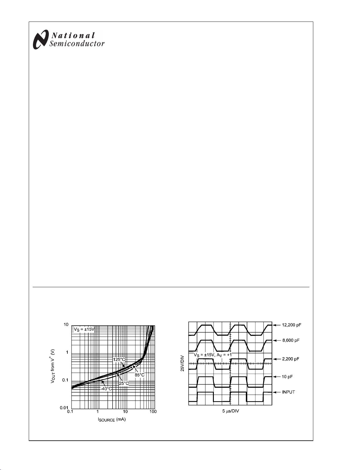
Typical Performance Characteristics
Output Swing vs. Sourcing Current
20205736
© 2008 National Semiconductor Corporation 202057 www.national.com
Large Signal Step Response
20205749
Page 2
Absolute Maximum Ratings (Note 1)
If Military/Aerospace specified devices are required,
please contact the National Semiconductor Sales Office/
Distributors for availability and specifications.
ESD Tolerance (Note 2)
LM7321/LM7322
Human Body Model 2 kV
Machine Model 200V
Charge-Device Model 1 kV
VIN Differential
Output Short Circuit Current (Note 3)
Supply Voltage (VS = V+ - V−)
Voltage at Input/Output pins V+ +0.8V, V− −0.8V
Storage Temperature Range −65°C to 150°C
±10V
35V
Junction Temperature (Note 4) 150°C
Soldering Information:
Infrared or Convection (20 sec.)
Wave Soldering (10 sec.)
Operating Ratings
Supply Voltage (VS = V+ - V−)
Temperature Range (Note 4) −40°C to 125°C
Package Thermal Resistance, θJA,(Note 4)
5-Pin SOT-23 325°C/W
8-Pin MSOP 235°C/W
8-Pin SOIC 165°C/W
2.7V Electrical Characteristics (Note 5)
Unless otherwise specified, all limits guaranteed for TA = 25°C, V+ = 2.7V, V− = 0V, VCM = 0.5V, V
RL > 1 MΩ to 1.35V. Boldface limits apply at the temperature extremes.
Symbol Parameter Condition Min
(Note 7)
V
OS
TC V
I
B
I
OS
CMRR Common Mode Rejection Ratio
PSRR Power Supply Rejection Ratio
CMVR Common Mode Voltage Range CMRR > 50 dB −0.3 −0.1
A
VOL
V
OUT
Input Offset Voltage VCM = 0.5V & VCM = 2.2V −5
−6
Input Offset Voltage Temperature Drift VCM = 0.5V & VCM = 2.2V
OS
Input Bias Current VCM = 0.5V
Input Offset Current VCM = 0.5V and VCM = 2.2V 20 200
Open Loop Voltage Gain
Output Voltage Swing
High
Output Voltage Swing
Low
(Note 8)
(Note 9)
VCM = 2.2V
(Note 9)
0V ≤ VCM ≤ 1.0V
0V ≤ VCM ≤ 2.7V
2.7V ≤ VS ≤ 30V
0.5V ≤ VO ≤ 2.2V
RL = 10 kΩ to 1.35V
0.5V ≤ VO ≤ 2.2V
RL = 2 kΩ to 1.35V
RL = 10 kΩ to 1.35V
VID = 100 mV
RL = 2 kΩ to 1.35V
VID = 100 mV
RL = 10 kΩ to 1.35V
VID = −100 mV
RL = 2 kΩ to 1.35V
VID = −100 mV
−2.0
−2.5
70
60
55
50
78
74
2.8
2.7
65
62
59
55
= 1.35V, and
OUT
Typ
(Note 6)
±0.7 +5
±2 µV/C
−1.2
0.45 1.0
100
70
104
3.0
72
66
50 150
100 250
20 120
40 120
2.5V to 32V
Max
(Note 7)
+6
1.5
300
0.0
160
280
150
150
235°C
260°C
Units
mV
µA
nA
dB
dB
V
dB
mV from
either rail
www.national.com 2
Page 3

LM7321/LM7322
Symbol Parameter Condition Min
(Note 7)
I
OUT
Output Current Sourcing
VID = 200 mV, V
= 0V (Note 3)
OUT
Sinking
VID = −200 mV, V
I
S
Supply Current LM7321 0.95 1.3
= 2.7V (Note 3)
OUT
LM7322 2.0 2.5
30
20
40
30
Typ
(Note 6)
48
65
Max
(Note 7)
1.9
Units
mA
mA
3.8
SR Slew Rate (Note 10) AV = +1, VI = 2V Step 8.5 V/µs
f
u
Unity Gain Frequency
RL = 2 kΩ, CL = 20 pF
7.5 MHz
GBW Gain Bandwidth f = 50 kHz 16 MHz
e
n
i
n
THD+N Total Harmonic Distortion + Noise V+ = 1.9V, V− = −0.8V
Input Referred Voltage Noise Density f = 2 kHz 11.9
Input Referred Current Noise Density f = 2 kHz 0.5
−77 dB
nV/
pA/
f = 1 kHz, RL = 100 kΩ, AV = +2
V
= 210 mV
CT Rej. Crosstalk Rejection
OUT
f = 100 kHz, Driver RL = 10 kΩ
PP
60 dB
±5V Electrical Characteristics (Note 5)
Unless otherwise specified, all limited guaranteed for TA = 25°C, V+ = 5V, V− = −5V, VCM = 0V, V
RL > 1 MΩ to 0V. Boldface limits apply at the temperature extremes.
Symbol Parameter Condition Min
(Note 7)
V
OS
TC V
Input Offset Voltage VCM = −4.5V and VCM = 4.5V −5
Input Offset Voltage Temperature Drift VCM = −4.5V and VCM = 4.5V
OS
(Note 8)
I
B
Input Bias Current VCM = −4.5V
(Note 9)
−2.0
−2.5
VCM = 4.5V
(Note 9)
I
OS
CMRR Common Mode Rejection Ratio
Input Offset Current VCM = −4.5V and VCM = 4.5V 20 200
−5V ≤ VCM ≤ 3V
−5V ≤ VCM ≤ 5V
PSRR Power Supply Rejection Ratio
2.7V ≤ VS ≤ 30V, VCM = −4.5V
CMVR Common Mode Voltage Range CMRR > 50 dB −5.3 −5.1
A
VOL
Open Loop Voltage Gain
−4V ≤ VO ≤ 4V
RL = 10 kΩ to 0V
−4V ≤ VO ≤ 4V
RL = 2 kΩ to 0V
= 0V, and
OUT
Typ
(Note 6)
Max
(Note 7)
Units
±0.7 +5
−6
+6
±2 µV/°C
−1.2
0.45 1.0
1.5
300
80
100
70
65
80
62
78
104
74
−5.0
5.1
5.3
5.0
74
80
70
68
74
65
mV
µA
nA
dB
dB
V
dB
3 www.national.com
Page 4
Symbol Parameter Condition Min
V
OUT
Output Voltage Swing
High
RL = 10 kΩ to 0V
VID = 100 mV
RL = 2 kΩ to 0V
LM7321/LM7322
Output Voltage Swing
Low
VID = 100 mV
RL = 10 kΩ to 0V
VID = −100 mV
RL = 2 kΩ to 0V
VID = −100 mV
I
OUT
Output Current Sourcing
VID = 200 mV, V
= −5V (Note 3)
OUT
Sinking
VID = −200 mV, V
I
S
Supply Current VCM = −4.5V LM7321 1.0 1.3
= 5V (Note 3)
OUT
(Note 7)
100 250
160 350
35 200
80 200
35
20
50
30
Typ
(Note 6)
70
85
Max
(Note 7)
280
450
250
250
2
LM7322 2.3 2.8
3.8
SR Slew Rate (Note 10) AV = +1, VI = 8V Step 12.3
f
u
Unity Gain Frequency
RL = 2 kΩ, CL = 20 pF
9 MHz
GBW Gain Bandwidth f = 50 kHz 16 MHz
e
n
i
n
THD+N Total Harmonic Distortion + Noise
CT Rej. Crosstalk Rejection
Input Referred Voltage Noise Density f = 2 kHz 14.3
Input Referred Current Noise Density f = 2 kHz 1.35
f = 1 kHz, RL = 100 kΩ, AV = +2
V
= 8 V
OUT
PP
f = 100 kHz, Driver RL = 10 kΩ
−79 dB
60 dB
Units
mV from
either rail
mA
mA
V/µs
nV/
pA/
±15V Electrical Characteristics (Note 5)
Unless otherwise specified, all limited guaranteed for TA = 25°C, V+ = 15V, V− = −15V, VCM = 0V, V
RL > 1MΩ to 15V. Boldface limits apply at the temperature extremes.
Symbol Parameter Condition
V
OS
Input Offset Voltage VCM = −14.5V and VCM = 14.5V −6
Min
(Note 7)
−8
TC V
Input Offset Voltage Temperature Drift VCM = −14.5V and VCM = 14.5V
OS
±2 µV/°C
(Note 8)
I
B
Input Bias Current VCM = −14.5V
(Note 9)
VCM = 14.5V
−2
−2.5
0.45 1.0
(Note 9)
I
OS
CMRR Common Mode Rejection Ratio
Input Offset Current VCM = −14.5V and VCM = 14.5V 30 300
−15V ≤ VCM ≤ 12V
80
75
−15V ≤ VCM ≤ 15V
72
70
PSRR Power Supply Rejection Ratio
2.7V ≤ VS ≤ 30V, VCM = −14.5V
78
74
CMVR Common Mode Voltage Range CMRR > 50 dB −15.3 −15.1
15.1
15
= 0V, and
OUT
Typ
(Note 6)
±0.7 +6
−1.1
100
80
100
15.3
Max
(Note 7)
+8
1.5
500
−15
Units
mV
µA
nA
dB
dB
V
www.national.com 4
Page 5
LM7321/LM7322
Symbol Parameter Condition
A
VOL
Open Loop Voltage Gain
−13V ≤ VO ≤ 13V
RL = 10 kΩ to 0V
−13V ≤ VO ≤ 13V
RL = 2 kΩ to 0V
V
OUT
Output Voltage Swing
High
RL = 10 kΩ to 0V
VID = 100 mV
RL = 2 kΩ to 0V
VID = 100 mV
Output Voltage Swing
Low
RL = 10 kΩ to 0V
VID = −100 mV
RL = 2 kΩ to 0V
VID = −100 mV
I
OUT
Output Current Sourcing
VID = 200 mV, V
OUT
Sinking
VID = −200 mV, V
I
S
Supply Current VCM = −14.5V LM7321 1.1 1.7
OUT
Min
(Note 7)
75
70
70
65
150 300
250 550
60 200
130 300
40 65
= −15V (Note 3)
60 100
= 15V (Note 3)
LM7322 2.5 4
Typ
(Note 6)
85
78
Max
(Note 7)
350
650
250
400
2.4
Units
dB
mV from
either rail
mA
mA
5.6
SR Slew Rate
(Note 10)
f
u
Unity Gain Frequency
AV = +1, VI = 20V Step 18
RL = 2 kΩ, CL = 20 pF
11.3 MHz
V/µs
GBW Gain Bandwidth f = 50 kHz 20 MHz
e
n
i
n
THD+N Total Harmonic Distortion +Noise
CT Rej. Crosstalk Rejection
Input Referred Voltage Noise Density f = 2 kHz 15
Input Referred Current Noise Density f = 2 kHz 1.3
f = 1 kHz,RL 100 kΩ,
AV = +2, V
OUT
= 23 V
PP
f = 100 kHz, Driver RL = 10 kΩ
−86 dB
60 dB
nV/
pA/
Note 1: Absolute Maximum Ratings indicate limits beyond which damage to the device may occur. Operating Rating indicate conditions for which the device is
intended to be functional, but specific performance is not guaranteed. For guaranteed specifications and the test conditions, see the Electrical Characteristics.
Note 2: Human Body Model, applicable std. MIL-STD-883, Method 3015.7. Machine Model, applicable std. JESD22-A115-A (ESD MM std. of JEDEC)
Field-Induced Charge-Device Model, applicable std. JESD22-C101-C (ESD FICDM std. of JEDEC).
Note 3: Applies to both single-supply and split-supply operation. Continuous short circuit operation at elevated ambient temperature can result in exceeding the
maximum allowed junction temperature of 150°C. Short circuit test is a momentary test. Output short circuit duration is infinite for VS ≤ 6V at room temperature
and below. For VS > 6V, allowable short circuit duration is 1.5 ms.
Note 4: The maximum power dissipation is a function of T
PD = (T
Note 5: Electrical Table values apply only for factory testing conditions at the temperature indicated. Factory testing conditions result in very limited self-heating
of the device such that TJ = TA. No guarantee of parametric performance is indicated in the electrical tables under conditions of internal self-heating where TJ >
TA.
Note 6: Typical values represent the most likely parametric norm as determined at the time of characterization. Actual typical values may vary over time and will
also depend on the application and configuration. The typical values are not tested and are not guaranteed on shipped production material.
Note 7: All limits are guaranteed by testing or statistical analysis.
Note 8: Offset voltage temperature drift determined by dividing the change in VOS at temperature extremes into the total temperature change.
Note 9: Positive current corresponds to current flowing into the device.
Note 10: Slew rate is the slower of the rising and falling slew rates. Connected as a Voltage Follower.
) - TA)/ θJA. All numbers apply for packages soldered directly onto a PC board.
J(MAX)
, θJA. The maximum allowable power dissipation at any ambient temperature is
J(MAX)
5 www.national.com
Page 6
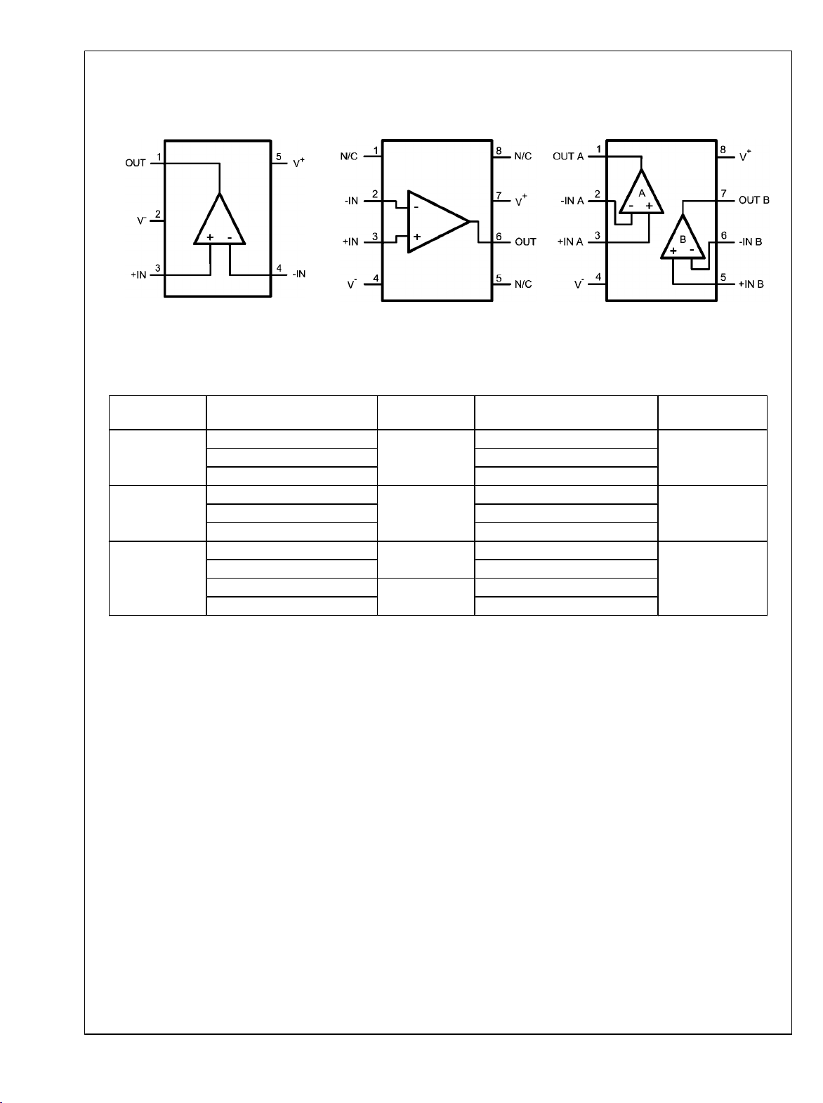
Connection Diagrams
5-Pin SOT-23
LM7321/LM7322
Top View
Ordering Information
Package Part Number Package
5-Pin SOT-23
8-Pin MSOP
8-Pin SOIC
8-Pin SOIC
20205705
Top View
Marking
LM7321MF
AU4A
LM7321MFX 3k Units Tape and Reel
LM7322MM
AZ4A
LM7322MMX 3.5k Units Tape and Reel
LM7321MA
LM7321MAX 2.5k Units Tape and Reel
LM7322MA LM7322MA 95 Units/Rail
LM7322MAX 2.5k Units Tape and Reel
LM7321MA
20205703
Media Transport NSC Drawing
1k Units Tape and Reel
1k Units Tape and Reel
95 Units/Rail
8-Pin MSOP/SOIC
Top View
20205706
MF05ALM7321MFE 250 Units Tape and Reel
MUA08ALM7322MME 250 Units Tape and Reel
M08A
www.national.com 6
Page 7
LM7321/LM7322
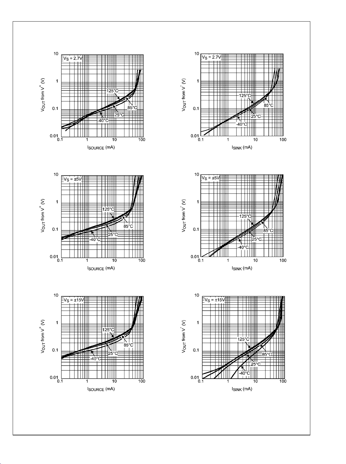
Typical Performance Characteristics Unless otherwise specified: T
Output Swing vs. Sourcing Current
20205734
Output Swing vs. Sourcing Current
Output Swing vs. Sinking Current
Output Swing vs. Sinking Current
= 25°C.
A
20205731
Output Swing vs. Sourcing Current
20205735
20205736
20205732
Output Swing vs. Sinking Current
20205733
7 www.national.com
Page 8
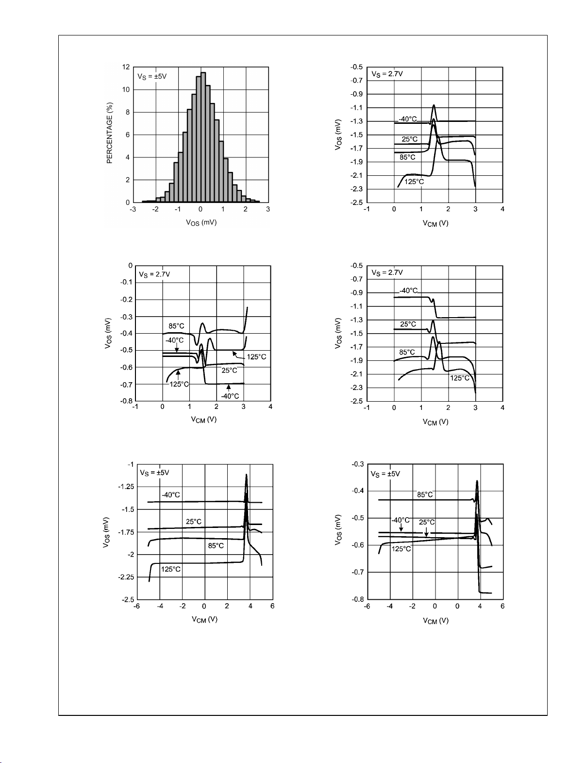
LM7321/LM7322
VOS Distribution
VOS vs. VCM (Unit 1)
VOS vs. VCM (Unit 2)
VOS vs. VCM (Unit 1)
20205730
20205708
20205707
VOS vs. VCM (Unit 3)
20205709
VOS vs. VCM (Unit 2)
20205710
www.national.com 8
20205711
Page 9

LM7321/LM7322
VOS vs. VCM (Unit 2)
VOS vs. VCM (Unit 2)
20205712
VOS vs. VCM (Unit 1)
20205713
VOS vs. VCM (Unit 3)
VOS vs. VS (Unit 1)
20205714
20205750
20205715
VOS vs. VS (Unit 2)
20205751
9 www.national.com
Page 10

LM7321/LM7322
VOS vs. VS (Unit 3)
VOS vs. VS (Unit 1)
VOS vs. VS (Unit 2)
I
vs. V
BIAS
CM
20205752
20205754
VOS vs. VS (Unit 3)
I
vs. V
BIAS
CM
20205753
20205755
20205723
www.national.com 10
20205724
Page 11

I
BIAS
vs. V
CM
I
BIAS
vs. V
LM7321/LM7322
S
I
vs. V
BIAS
S
IS vs. VCM (LM7322)
20205725
20205721
20205722
IS vs. VCM (LM7321)
20205718
IS vs. VCM (LM7321)
20205775
20205719
11 www.national.com
Page 12

LM7321/LM7322
IS vs. VCM (LM7322)
IS vs. VCM (LM7321)
IS vs. VCM (LM7322)
IS vs. VS (LM7322)
20205776
20205777
20205720
IS vs. VS (LM7321)
20205717
IS vs. VS (LM7321)
20205779
www.national.com 12
20205716
Page 13

LM7321/LM7322
IS vs. VS (LM7322)
20205778
Positive Output Swing vs. Supply Voltage
Positive Output Swing vs. Supply Voltage
20205727
Negative Output Swing vs. Supply Voltage
20205726
Negative Output Swing vs. Supply Voltage
20205729
20205728
Open Loop Frequency Response with Various Capacitive
Load
20205782
13 www.national.com
Page 14

Open Loop Frequency Response with Various Resistive
Load
LM7321/LM7322
Open Loop Frequency Response with Various Supply
Voltage
Phase Margin vs. Capacitive Load
+PSRR vs. Frequency
20205783
20205738
20205784
CMRR vs. Frequency
20205739
−PSRR vs. Frequency
20205740
www.national.com 14
20205741
Page 15

LM7321/LM7322
Small Signal Step Response
20205737
Input Referred Noise Density vs. Frequency
Large Signal Step Response
20205749
Input Referred Noise Density vs. Frequency
Input Referred Noise Density vs. Frequency
20205742
20205744
20205743
THD+N vs. Frequency
20205745
15 www.national.com
Page 16

LM7321/LM7322
THD+N vs. Output Amplitude
THD+N vs. Output Amplitude
THD+N vs. Output Amplitude
20205746
20205748
20205747
Crosstalk Rejection vs. Frequency
20205768
www.national.com 16
Page 17

Application Information
DRIVING CAPACITIVE LOADS
The LM7321/LM7322 are specifically designed to drive unlimited capacitive loads without oscillations as shown in
Figure 1.
20205769
FIGURE 1. ±5% Settling Time vs. Capacitive Load
In addition, the output current handling capability of the device
allows for good slewing characteristics even with large capacitive loads as shown in Figure 2 and Figure 3.
20205770
FIGURE 2. +SR vs. Capacitive Load
LM7321/LM7322
20205771
FIGURE 3. −SR vs. Capacitive Load
The combination of these features is ideal for applications
such as TFT flat panel buffers, A/D converter input amplifiers,
etc.
However, as in most op amps, addition of a series isolation
resistor between the op amp and the capacitive load improves
the settling and overshoot performance.
Output current drive is an important parameter when driving
capacitive loads. This parameter will determine how fast the
output voltage can change. Referring to the Slew Rate vs.
Capacitive Load Plots (typical performance characteristics
section), two distinct regions can be identified. Below about
10,000 pF, the output Slew Rate is solely determined by the
op amp’s compensation capacitor value and available current
into that capacitor. Beyond 10 nF, the Slew Rate is determined by the op amp’s available output current. Note that
because of the lower output sourcing current compared to the
sinking one, the Slew Rate limit under heavy capacitive loading is determined by the positive transitions. An estimate of
positive and negative slew rates for loads larger than 100 nF
can be made by dividing the short circuit current value by the
capacitor.
For the LM7321/LM7322, the available output current increases with the input overdrive. Referring to Figure 4 and
Figure 5, Output Short Circuit Current vs. Input Overdrive, it
can be seen that both sourcing and sinking short circuit current increase as input overdrive increases. In a closed loop
amplifier configuration, during transient conditions while the
fed back output has not quite caught up with the input, there
will be an overdrive imposed on the input allowing more output
current than would normally be available under steady state
condition. Because of this feature, the op amp’s output stage
quiescent current can be kept to a minimum, thereby reducing
power consumption, while enabling the device to deliver large
output current when the need arises (such as during transients).
17 www.national.com
Page 18

LM7321/LM7322
FIGURE 4. Output Short Circuit Sourcing Current vs.
Input Overdrive
20205774
FIGURE 6. Buffer Amplifier Scope Photo
20205772
ESTIMATING THE OUTPUT VOLTAGE SWING
It is important to keep in mind that the steady state output
current will be less than the current available when there is
an input overdrive present. For steady state conditions, the
Output Voltage vs. Output Current plot (Typical Performance
Characteristics section) can be used to predict the output
swing. Figure 7 and Figure 8 show this performance along
with several load lines corresponding to loads tied between
the output and ground. In each cases, the intersection of the
device plot at the appropriate temperature with the load line
would be the typical output swing possible for that load. For
example, a 1 kΩ load can accommodate an output swing to
within 250 mV of V− and to 330 mV of V+ (VS = ±15V) corresponding to a typical 29.3 VPP unclipped swing.
20205773
FIGURE 5. Output Short Circuit Sinking Current vs. Input
Overdrive
Figure 6 shows the output voltage, output current, and the
resulting input overdrive with the device set for AV = +1 and
the input tied to a 1 VPP step function driving a 47 nF capacitor.
As can be seen, during the output transition, the input overdrive reaches 1V peak and is more than enough to cause the
output current to increase to its maximum value (see Figure
4 and Figure 5 plots). Note that because of the larger output
sinking current compared to the sourcing one, the output negative transition is faster than the positive one.
www.national.com 18
20205756
FIGURE 7. Output Sourcing Characteristics with Load
Lines
Page 19

20205759
LM7321/LM7322
20205757
FIGURE 8. Output Sinking Characteristics with Load
Lines
SETTLING TIME WITH LARGE CAPACITIVE LOADS
Figure 9 below, shows a typical application where the
LM7321/LM7322 is used as a buffer amplifier for the V
signal employed in a TFT LCD flat panel:
FIGURE 9. V
Driver Application Schematic
COM
COM
20205758
Figure 10 shows the time domain response of the amplifier
when used as a V
application, the op amp loop will try and maintain its output
buffer/driver with V
COM
at ground. In this
REF
voltage based on the voltage on its non-inverting input
(V
) despite the current injected into the TFT simulated
REF
load. As long as this load current is within the range tolerable
by the LM7321/LM7322 (45 mA sourcing and 65 mA sinking
for ±5V supplies), the output will settle to its final value within
less than 2 μs.
FIGURE 10. V
Driver Performance Scope Photo
COM
OUTPUT SHORT CIRCUIT CURRENT AND DISSIPATION ISSUES
The LM7321/LM7322 output stage is designed for maximum
output current capability. Even though momentary output
shorts to ground and either supply can be tolerated at all operating voltages, longer lasting short conditions can cause the
junction temperature to rise beyond the absolute maximum
rating of the device, especially at higher supply voltage conditions. Below supply voltage of 6V, the output short circuit
condition can be tolerated indefinitely.
With the op amp tied to a load, the device power dissipation
consists of the quiescent power due to the supply current flow
into the device, in addition to power dissipation due to the load
current. The load portion of the power itself could include an
average value (due to a DC load current) and an AC component. DC load current would flow if there is an output voltage
offset, or the output AC average current is non-zero, or if the
op amp operates in a single supply application where the output is maintained somewhere in the range of linear operation.
Therefore:
P
= PQ + PDC + P
TOTAL
PQ = IS · V
S
AC
Op Amp Quiescent Power
Dissipation
PDC = IO · (Vr - Vo) DC Load Power
PAC = See Table 1 below AC Load Power
where:
IS: Supply Current
VS: Total Supply Voltage (V+ − V−)
VO: Average Output Voltage
Vr: V+ for sourcing and V− for sinking current
19 www.national.com
Page 20

Table 1 below shows the maximum AC component of the load
power dissipated by the op amp for standard Sinusoidal, Triangular, and Square Waveforms:
TABLE 1. Normalized AC Power Dissipated in the Output
Stage for Standard Waveforms
LM7321/LM7322
PAC (W.Ω/V2)
Sinusoidal Triangular Square
50.7 x 10
−3
46.9 x 10
The table entries are normalized to V
AC load current component of power dissipation, simply mul-
−3
62.5 x 10
2
/RL. To figure out the
S
tiply the table entry corresponding to the output waveform by
2
the factor V
load, and triangular waveform power dissipation in the output
/RL. For example, with ±12V supplies, a 600Ω
S
stage is calculated as:
PAC = (46.9 x 10−3) · [242/600] = 45.0 mW
The maximum power dissipation allowed at a certain temperature is a function of maximum die junction temperature (T
) allowed, ambient temperature TA, and package thermal
(MAX)
resistance from junction to ambient, θJA.
For the LM7321/LM7322, the maximum junction temperature
allowed is 150°C at which no power dissipation is allowed.
The power capability at 25°C is given by the following calculations:
For MSOP package:
For SOIC package:
−3
20205765
FIGURE 11. Power Capability vs. Temperature
J
When high power is required and ambient temperature can't
be reduced, providing air flow is an effective approach to reduce thermal resistance therefore to improve power capability.
Other Application Hints
The use of supply decoupling is mandatory in most applications. As with most relatively high speed/high output current
Op Amps, best results are achieved when each supply line is
decoupled with two capacitors; a small value ceramic capacitor (∼0.01 μF) placed very close to the supply lead in addition
to a large value Tantalum or Aluminum (> 4.7 μF). The large
capacitor can be shared by more than one device if necessary. The small ceramic capacitor maintains low supply
impedance at high frequencies while the large capacitor will
act as the charge "bucket" for fast load current spikes at the
op amp output. The combination of these capacitors will provide supply decoupling and will help keep the op amp oscillation free under any load.
Similarly, the power capability at 125°C is given by:
For MSOP package:
For SOIC package:
Figure 11 shows the power capability vs. temperature for
MSOP and SOIC packages. The area under the maximum
thermal capability line is the operating area for the device.
When the device works in the operating area where P
less than P
below 150°C. If the intersection of ambient temperature and
, the device junction temperature will remain
D(MAX)
TOTAL
is
package power is above the maximum thermal capability line,
the junction temperature will exceed 150°C and this should
be strictly prohibited.
www.national.com 20
SIMILAR HIGH OUTPUT DEVICES
The LM7332 is a dual rail-to-rail amplifier with a slightly lower
GBW capable of sinking and sourcing 100 mA. It is available
in SOIC and MSOP packages.
The LM4562 is dual op amp with very low noise and 0.7 mV
voltage offset.
The LME49870 and LME49860 are single and dual low noise
amplifiers that can work from ±22 volt supplies.
OTHER HIGH PERFORMANCE SOT-23 AMPLIERS
The LM7341 is a 4 MHz rail-to-rail input and output part that
requires only 0.6 mA to operate, and can drive unlimited capacitive load. It has a voltage gain of 97 dB, a CMRR of 93
dB, and a PSRR of 104 dB.
The LM6211 is a 20 MHz part with CMOS input, which runs
on ±12 volt or 24 volt single supplies. It has rail-to-rail output
and low noise.
The LM7121 has a gain bandwidth of 235 MHz.
Detailed information on these parts can be found at
www.national.com.
Page 21

Physical Dimensions inches (millimeters) unless otherwise noted
LM7321/LM7322
NS Package Number MF05A
5-Pin SOT-23
NS Package Number MUA08A
8-Pin MSOP
21 www.national.com
Page 22

LM7321/LM7322
NS Package Number M08A
8-Pin SOIC
www.national.com 22
Page 23

Notes
LM7321/LM7322
23 www.national.com
Page 24

Notes
For more National Semiconductor product information and proven design tools, visit the following Web sites at:
Products Design Support
Amplifiers www.national.com/amplifiers WEBENCH www.national.com/webench
Audio www.national.com/audio Analog University www.national.com/AU
Clock Conditioners www.national.com/timing App Notes www.national.com/appnotes
Data Converters www.national.com/adc Distributors www.national.com/contacts
Displays www.national.com/displays Green Compliance www.national.com/quality/green
Ethernet www.national.com/ethernet Packaging www.national.com/packaging
Interface www.national.com/interface Quality and Reliability www.national.com/quality
LVDS www.national.com/lvds Reference Designs www.national.com/refdesigns
Power Management www.national.com/power Feedback www.national.com/feedback
Switching Regulators www.national.com/switchers
LDOs www.national.com/ldo
LED Lighting www.national.com/led
Capacitive Load Operational Amplifier
PowerWise www.national.com/powerwise
Serial Digital Interface (SDI) www.national.com/sdi
Temperature Sensors www.national.com/tempsensors
Wireless (PLL/VCO) www.national.com/wireless
THE CONTENTS OF THIS DOCUMENT ARE PROVIDED IN CONNECTION WITH NATIONAL SEMICONDUCTOR CORPORATION
(“NATIONAL”) PRODUCTS. NATIONAL MAKES NO REPRESENTATIONS OR WARRANTIES WITH RESPECT TO THE ACCURACY
OR COMPLETENESS OF THE CONTENTS OF THIS PUBLICATION AND RESERVES THE RIGHT TO MAKE CHANGES TO
SPECIFICATIONS AND PRODUCT DESCRIPTIONS AT ANY TIME WITHOUT NOTICE. NO LICENSE, WHETHER EXPRESS,
IMPLIED, ARISING BY ESTOPPEL OR OTHERWISE, TO ANY INTELLECTUAL PROPERTY RIGHTS IS GRANTED BY THIS
DOCUMENT.
TESTING AND OTHER QUALITY CONTROLS ARE USED TO THE EXTENT NATIONAL DEEMS NECESSARY TO SUPPORT
NATIONAL’S PRODUCT WARRANTY. EXCEPT WHERE MANDATED BY GOVERNMENT REQUIREMENTS, TESTING OF ALL
PARAMETERS OF EACH PRODUCT IS NOT NECESSARILY PERFORMED. NATIONAL ASSUMES NO LIABILITY FOR
APPLICATIONS ASSISTANCE OR BUYER PRODUCT DESIGN. BUYERS ARE RESPONSIBLE FOR THEIR PRODUCTS AND
APPLICATIONS USING NATIONAL COMPONENTS. PRIOR TO USING OR DISTRIBUTING ANY PRODUCTS THAT INCLUDE
NATIONAL COMPONENTS, BUYERS SHOULD PROVIDE ADEQUATE DESIGN, TESTING AND OPERATING SAFEGUARDS.
EXCEPT AS PROVIDED IN NATIONAL’S TERMS AND CONDITIONS OF SALE FOR SUCH PRODUCTS, NATIONAL ASSUMES NO
LIABILITY WHATSOEVER, AND NATIONAL DISCLAIMS ANY EXPRESS OR IMPLIED WARRANTY RELATING TO THE SALE
AND/OR USE OF NATIONAL PRODUCTS INCLUDING LIABILITY OR WARRANTIES RELATING TO FITNESS FOR A PARTICULAR
PURPOSE, MERCHANTABILITY, OR INFRINGEMENT OF ANY PATENT, COPYRIGHT OR OTHER INTELLECTUAL PROPERTY
RIGHT.
LIFE SUPPORT POLICY
NATIONAL’S PRODUCTS ARE NOT AUTHORIZED FOR USE AS CRITICAL COMPONENTS IN LIFE SUPPORT DEVICES OR
SYSTEMS WITHOUT THE EXPRESS PRIOR WRITTEN APPROVAL OF THE CHIEF EXECUTIVE OFFICER AND GENERAL
COUNSEL OF NATIONAL SEMICONDUCTOR CORPORATION. As used herein:
Life support devices or systems are devices which (a) are intended for surgical implant into the body, or (b) support or sustain life and
whose failure to perform when properly used in accordance with instructions for use provided in the labeling can be reasonably expected
to result in a significant injury to the user. A critical component is any component in a life support device or system whose failure to perform
can be reasonably expected to cause the failure of the life support device or system or to affect its safety or effectiveness.
National Semiconductor and the National Semiconductor logo are registered trademarks of National Semiconductor Corporation. All other
brand or product names may be trademarks or registered trademarks of their respective holders.
Copyright© 2008 National Semiconductor Corporation
For the most current product information visit us at www.national.com
National Semiconductor
Americas Technical
Support Center
Email: support@nsc.com
LM7321 Single/ LM7322 Dual Rail-to-Rail Input/Output, ±15V, High Output Current and Unlimited
www.national.com
Tel: 1-800-272-9959
National Semiconductor Europe
Technical Support Center
Email: europe.support@nsc.com
German Tel: +49 (0) 180 5010 771
English Tel: +44 (0) 870 850 4288
National Semiconductor Asia
Pacific Technical Support Center
Email: ap.support@nsc.com
National Semiconductor Japan
Technical Support Center
Email: jpn.feedback@nsc.com
 Loading...