

National Semiconductor LM725 Technical data
查询LM725供应商
LM725
Operational Amplifier
LM725 Operational Amplifier
May 1998
General Description
The LM725/LM725A/LM725C are operational amplifiers featuring superior performance in applications where low noise,
low drift, and accurate closed-loop gain are required. With
high common mode rejection and offset null capability, it is
especially suited for low level instrumentation applications
over a wide supply voltage range.
The LM725A has tightened electrical performance with
higher input accuracy and like the LM725, is guaranteed
over a −55˚C to +125˚C temperature range. The LM725C
has slightly relaxed specifications and has its performance
guaranteed over a 0˚C to 70˚C temperature range.
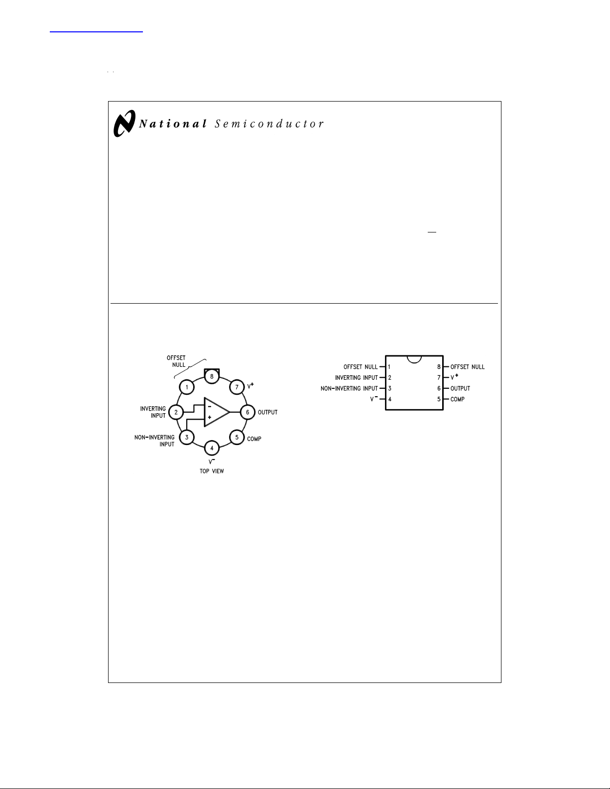
Connection Diagrams
Metal Can Package
DS010474-1
Order Number LM725H/883, LM725CH
or LM725AH/883
See NS Package Number H08C
Features
n High open loop gain 3,000,000
n Low input voltage drift 0.6 µV/˚C
n High common mode rejection 120 dB
n Low input noise current 0.15 pA/
n Low input offset current 2 nA
n High input voltage range
n Wide power supply range
n Offset null capability
n Output short circuit protection
Dual-In-Line Package
Order Number LM725CN
See NS Package Number N08E
±
14V
±
3V to±22V
√
Hz
DS010474-2
© 1999 National Semiconductor Corporation DS010474 www.national.com
Absolute Maximum Ratings (Note 1)
If Military/Aerospace specified devices are required,
please contact theNationalSemiconductor Sales Office/
Distributors for availability and specifications.
Supply Voltage
Internal Power Dissipation (Note 2) 500 mW
Differential Input Voltage
Input Voltage (Note 3)
±
22V
±
±
22V
Lead Temperature
(Soldering, 10 Sec.) 260˚C
Maximum Junction Temperature 150˚C
Operating Temperature Range T
A(MIN)
LM725 −55˚C to +125˚C
5V
LM725A −55˚C to +125˚C
LM725C 0˚C to +70˚C
T
A(MAX)
Storage Temperature Range −65˚C to +150˚C
Electrical Characteristics (Note 4)
Parameter Conditions LM725A LM725 LM725C Units
Min Typ Max Min Typ Max Min Typ Max
Input Offset Voltage T
(Without External Trim) R
Input Offset Current T
Input Bias Current T
Input Noise Voltage T
Input Noise Current T
Input Resistance T
Input Voltage Range T
Large Signal Voltage
Gain
Common-Mode T
Rejection Ratio R
Power Supply T
Rejection Ratio R
Output Voltage Swing T
Power Consumption T
Input Offset Voltage R
(Without External Trim)
Average Input Offset R
Voltage Drift 2.0 2.0 5.0 2.0 µV/˚C
(Without External Trim)
Average Input Offset R
Voltage Drift 0.6 1.0 0.6 0.6 µV/˚C
(With External Trim)
Input Offset Current T
Average Input Offset 35 90 35 150 10 pA/˚C
Current Drift
Input Bias Current T
=
25˚C, 0.5 0.5 1.0 0.5 2.5 mV
A
≤ 10 kΩ
S
=
25˚C 2.0 5.0 2.0 20 2.0 35 nA
A
=
25˚C 42 80 42 100 42 125 nA
A
=
25˚C
A
=
f
10 Hz 15 15 15 nV/
o
=
f
100 Hz 9.0 9.0 9.0 nV/
o
=
f
1 kHz 8.0 8.0 8.0 nV/
o
=
25˚C
A
=
f
10 Hz 1.0 1.0 1.0 pA/
o
=
f
100 Hz 0.3 0.3 0.3 pA/
o
=
f
1 kHz 0.15 0.15 0.15 pA/
o
=
25˚C 1.5 1.5 1.5 MΩ
A
=
25˚C
A
=
T
25˚C,
A
R
≥ 2kΩ, 1000 3000 1000 3000 250 3000 V/mV
L
=
±
V
OUT
=
25˚C, 120 110 120 94 120 dB
A
≤ 10 kΩ
S
=
25˚C, 2.0 5.0 2.0 10 2.0 35 µV/V
A
≤ 10 kΩ
S
=
25˚C,
A
R
≥ 10 kΩ
L
R
≥ 2kΩ
L
=
25˚C 80 105 80 105 80 150 mW
A
≤ 10 kΩ 0.7 1.5 3.5 mV
S
=
50Ω
S
=
50Ω
S
=
T
A
MAX
=
T
T
A
MIN
=
T
A
MAX
=
T
T
A
MIN
10V
±
13.5
±
12.5±13.5
±
12.0±13.5
±
14
±
13.5
±
12±13.5
±
10±13.5
±
14
±
13.5±14 V
±12±
13.5 V
±10±
13.5 V
1.2 4.0 1.2 20 1.2 35 nA
7.5 18.0 7.5 40 4.0 50 nA
20 70 20 100 125 nA
80 180 80 200 250 nA
√
√
√
√
√
√
Hz
Hz
Hz
Hz
Hz
Hz
www.national.com 2
Electrical Characteristics (Note 4) (Continued)
Parameter Conditions LM725A LM725 LM725C Units
Min Typ Max Min Typ Max Min Typ Max
Large Signal Voltage
Gain
Common-Mode R
R
≥ 2kΩ
L
=
T
T
A
MAX
R
≥ 2kΩ
L
=
T
T
A
MIN
≤ 10 kΩ 110 100 115 dB
S
1,000,000 1,000,000 125,000 V/V
500,000 250,000 125,000 V/V
Rejection Ratio
Power Supply R
≤ 10 kΩ 8.0 20 20 µV/V
S
Rejection Ratio
Output Voltage Swing R
Note 1: “Absolute Maximum Ratings” indicate limits beyond which damage to the device may occur. Operating Ratings indicate conditions for which the device is
functional, but do not guarantee specific performance limits.
Note 2: Derate at 150˚C/W for operation at ambient temperatures above 75˚C.
Note 3: For supply voltages less than
Note 4: These specifications apply for V
Note 5: For Military electrical specifications RETS725AX are available for LM725AH and RETS725X are available for LM725H.
≥ 2kΩ
L
±
22V, the absolute maximum input voltage is equal to the supply voltage.
=
±
15V unless otherwise specified.
S
±
12
±
10
±
10 V
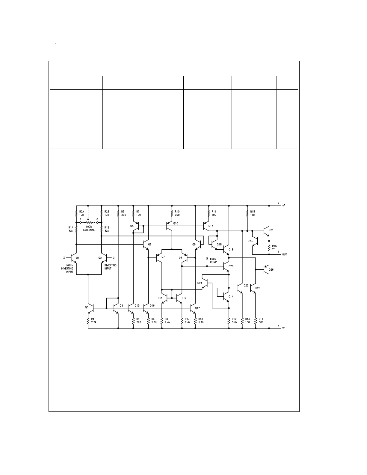
Schematic Diagram
DS010474-5
www.national.com3
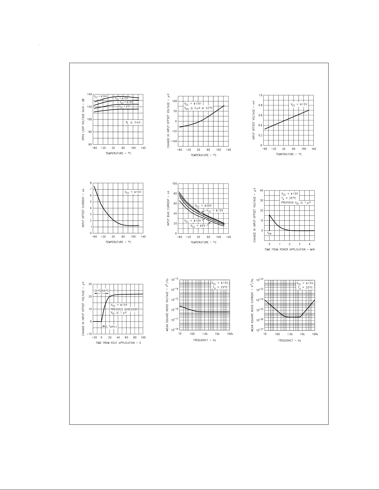
Typical Performance Characteristics
Voltage Gain vs Temperature
for Supply Voltages
DS010474-15
Input Offset Current
vs Temperature
DS010474-18
Change in Trimmed Input
Offset Voltage vs Temperature
DS010474-16
Input Bias Current
vs Temperature
DS010474-19
Untrimmed Input Offset
Voltage vs Temperature
DS010474-17
Stabilization Time of
Input Offset Voltage
from Power Turn-On
DS010474-20
Change in Input
Offset Voltage Due to
Thermal Shock vs Time
DS010474-21
www.national.com 4
Input Noise
Voltage vs Frequency
DS010474-22
Input Noise
Current vs Frequency
DS010474-23
 Loading...