

查询LM7131供应商
LM7131
Tiny High Speed Single Supply Operational Amplifier
General Description
The LM7131 is a high speed bipolar operational amplifier
available in a tiny SOT23-5 package. This makes the
LM7131 ideal for space and weight critical designs. Single
supply voltages of 3V and 5V provides good video performance, wide bandwidth, low distortion, and high PSRR and
CMRR. This makes the amplifier an excellent choice for
desktop and portable video and computing applications. The
amplifier is supplied in surface mount 8-pin and tiny
SOT23-5 packages.
Tiny amplifiers are so small they can be placed anywhere on
a board close to the signal source or next to an A-to-D input.
Good high speed performance at low voltage makes the
LM7131 a preferred part for battery powered designs.
Features
n Tiny SOT23-5 package saves space-typical circuit
layouts take half the space of SO-8 designs.
September 1999
n Guaranteed specs at 3V, 5V, and
n Typical supply current 7.0 mA at 5V, 6.5 mA at 3V
n 4V output swing with +5V single supply
n Typical total harmonic distortion of 0.1%at 4 MHz
n 70 MHz Gain-Bandwidth Product
n 90 MHz −3 dB bandwidth at 3V and 5V, Gain=+1
n Designed to drive popular video A/D converters
n 40 mA output can drive 50Ω loads
n Differential gain and phase 0.25%and 0.75˚ at A
±
5V supplies
Applications
n Driving video A/D converters
n Video output for portable computers and PDAs
n Desktop teleconferencing
n High fidelity digital audio
n Video cards
LM7131 Tiny High Speed Single Supply Operational Amplifier
=
+2
V
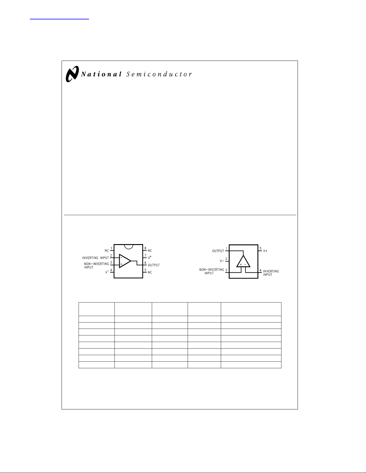
Connection Diagrams
8-Pin SO-8
DS012313-1
Top View
Package Ordering NSC Drawing Package Supplied as
Information Number Marking
8-Pin SO-8 LM7131ACM M08A LM7131ACM rails
8-Pin SO-8 LM7131BCM M08A LM7131BCM rails
8-Pin SO-8 LM7131ACMX M08A LM7131ACM 2.5k units tape and reel
8-Pin SO-8 LM7131BCMX M08A LM7131BCM 2.5k units tape and reel
5-Pin SOT 23-5 LM7131ACM5 MA05A A02A 1k units on tape and reel
5-Pin SOT 23-5 LM7131BCM5 MA05A A02B 1k units on tape and reel
5-Pin SOT 23-5 LM7131ACM5X MA05A A02A 3k units tape and reel
5-Pin SOT 23-5 LM7131BCM5X MA05A A02B 3k units tape and reel
5-Pin SOT23-5
Top View
DS012313-2
© 1999 National Semiconductor Corporation DS012313 www.national.com
Absolute Maximum Ratings (Note 1)
If Military/Aerospace specified devices are required,
please contact the NationalSemiconductorSalesOffice/
Distributors for availability and specifications.
ESD Tolerance (Note 2) 2000V
Differential Input Voltage
Voltage at Input/Output Pin (V
Supply Voltage (V
+–V−
) 12V
+
)+0.1V, (V−) − 0.3V
Current at Input Pin
Current at Output Pin (Note 3)
Current at Power Supply Pin
Lead Temperature
±
±
80 mA
±
80 mA
±
2.0
5mA
(soldering, 10 sec) 260˚C
Storage Temperature Range − 65˚C to +150˚C
Junction Temperature (Note 4) 150˚C
Operating Ratings
Supply Voltage (V+–V−) 2.7V ≤ V ≤ 12V
Junction Temperature Range
LM7131AC, LM7131BC 0˚C ≤ T
Thermal Resistance (θ
)
JA
SO-8 Package, 8-Pin Surface Mount 165˚C/W
M05A Package, 5-Pin Surface Mount 325˚C/W
≤ + 70˚C
J
3V DC Electrical Characteristics
Unless otherwise specified, all limits guaranteed for T
face limits apply at the temperature extremes.
Symbol Parameter Conditions Typ
V
OS
TCV
Input Offset Voltage 0.02 3.5 7 mV
Input Offset Voltage 10 µV/˚C
OS
=
J
25˚C, V
+
=
3V, V
−
=
(Note 5)
Average Drift
I
B
I
OS
CMRR Common Mode 0V ≤ V
Input Bias Current 20 35 35 µA
Input Offset Current 0.35 3.5 3.5 µA
≤ 0.85V 75 60 60 dB
CM
Rejection Ratio (Video Levels) 55 55 min
CMRR Common Mode 0.85V ≤ V
≤ 1.7V 70 55 55 dB
CM
Rejection Ratio (Mid-Range) 50 50 min
+PSRR Positive Power Supply V
Rejection Ratio V
−PSRR Negative Power Supply V
Rejection Ratio V
V
CM
Input Common-Mode V
=
+
=
−
=
−
=
+
=
=
3V, V
0V 75 65 65 dB
3V to 6.5V 60 60 min
+
=
−3V, V
0V 75 65 65 dB
−3V to −6.5V 60 60 min
3V 0.0 0.0 0.0 V
+
−
Voltage Range For CMRR ≥ 50 dB 0.00 0.00 min
2.0 1.70 1.70 V
A
VOL
Voltage Gain R
=
L
150Ω,V
=
0.250V 60 55 55 dB
O
to 1.250V 50 50
C
IN
Common-Mode 2 pF
Input Capacitance
+
V
O
Output Swing V
=
3V, R
=
150Ω 2.6 2.3 2.3 V
L
High terminated at 0V 2.0 2.0 min
Low V
=
3V, R
=
150Ω 0.05 0.15 0.15 V
L
+
terminated at 0V 0.20 0.20 max
High V
=
3V, R
=
150Ω 2.6 2.3 2.3 V
L
+
terminated at 1.5V 2.0 2.0 min
Low V
=
3V, R
=
150Ω 0.5 0.8 0.8 V
L
+
terminated at 1.5V 1.0 1.0 max
+
V
O
Output Swing V
=
3V, R
=
600Ω 2.73 V
L
High terminated at 0V max
+
=
=
0V, V
CM
/2 and R
V
V
O
LM7131AC LM7131BC Units
Limit Limit
(Note 6) (Note 6)
410max
40 40 max
55max
1.60 1.60 max
=
150Ω. Bold-
L
www.national.com 2
3V DC Electrical Characteristics (Continued)
Unless otherwise specified, all limits guaranteed for T
face limits apply at the temperature extremes.
=
J
25˚C, V
+
Symbol Parameter Conditions Typ
+
V
O
Output Swing V
=
3V, R
=
600Ω 0.06 V
L
Low terminated at 0V max
I
SC
Output Short Circuit Sourcing, V
=
0V 65 45 45 mA
O
Current 40 40 min
Sinking, V
I
S
Supply Current V
+
=
3V 40 25 25 mA
O
=
+ 3V 6.5 9.0 9.0 mA
=
3V, V
−
=
(Note 5)
0V, V
=
CM
+
=
/2 and R
V
V
O
LM7131AC LM7131BC Units
Limit Limit
(Note 6) (Note 6)
20 20 min
9.5 9.5 max
=
150Ω. Bold-
L
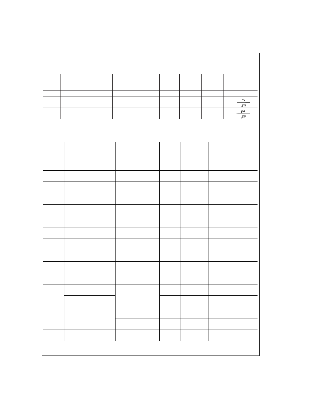
3V AC Electrical Characteristics
Unless otherwise specified, all limits guaranteed for T
face limits apply at the temperature extremes.
Symbol Parameter Conditions Typ
=
J
25˚C, V
+
=
3V, V
−
=
(Note 5)
0V, V
=
CM
+
=
/2 and R
V
V
O
=
150Ω. Bold-
L
LM7131AC LM7131BC Units
Limit Limit
(Note 6) (Note 6)
T.H.D. Total Harmonic Distortion F=4 MHz, A
=
R
150Ω,V
L
Differential Gain (Note 10) 0.45
=
+ 2 0.1
V
=
1.0V
O
PP
%
%
Differential Phase (Note 10) 0.6 ˚
SR Slew Rate R
=
L
150Ω,C
=
5 pF 120 V/µS
L
(Note 7)
SR Slew Rate R
=
L
150Ω,C
=
20 pF 100 V/µS
L
(Note 7)
GBW Gain-Bandwidth Product 70 MHz
Closed-Loop−3dB 90 MHz
Bandwidth
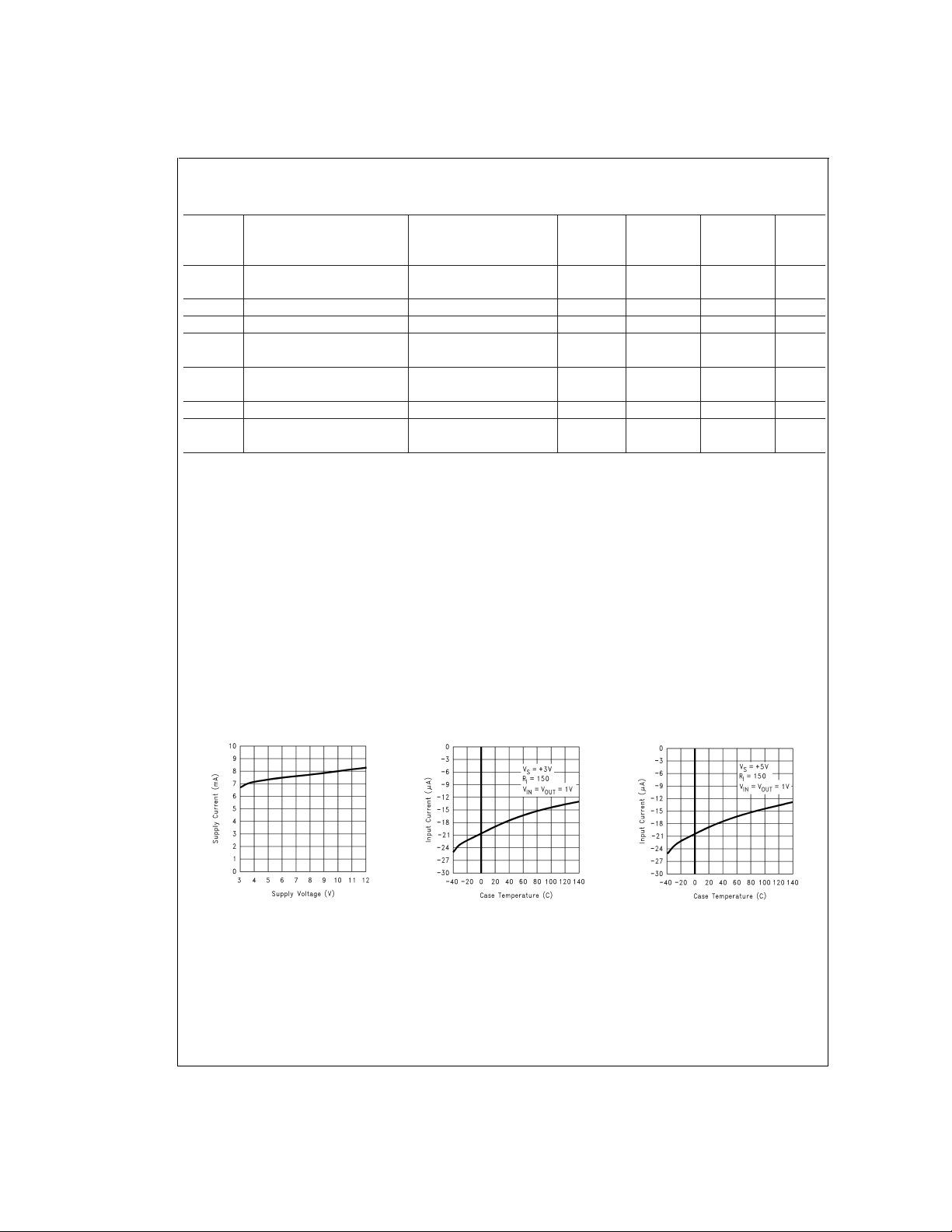
5V DC Electrical Characteristics
Unless otherwise specified, all limits guaranteed for T
face limits apply at the temperature extremes.
Symbol Parameter Conditions Typ
=
J
25˚C, V
+
=
5V, V
−
=
(Note 5)
0V, V
=
/2 and R
V
CM
V
O
=
L
+
=
LM7131AC LM7131BC Units
Limit Limit
150Ω. Bold-
(Note 6) (Note 6)
V
OS
Input Offset Voltage 0.02 3.5 7 mV
410max
TCV
OS
Input Offset Voltage 10 µV/˚C
Average Drift
I
B
Input Bias Current 20 35 35 µA
40 40 max
I
OS
Input Offset Current 0.35 3.5 3.5 µA
55max
CMRR Common Mode 0V ≤ V
≤ 1.85V 75 65 65 dB
CM
Rejection Ratio (Video Levels) 60 60 min
CMRR Common Mode 1.85V ≤ V
≤ 3.7V 70 55 55 dB
CM
Rejection Ratio (Mid-Range) 50 50 min
+ PSRR Positive Power Supply V
+
=
5V, V
−
=
0V 75 65 65 dB
www.national.com3
5V DC Electrical Characteristics (Continued)
Unless otherwise specified, all limits guaranteed for T
face limits apply at the temperature extremes.
=
J
25˚C, V
+
Symbol Parameter Conditions Typ
+
=
Rejection Ratio V
− PSRR Negative Power Supply V
Rejection Ratio V
V
CM
Input Common-Mode V
5V to 10V 60 60 min
−
=
−
=
+
=
+
− 5V, V
=
0V 75 65 65 dB
− 5V to −10V 60 60 min
5V 0.0 − 0.0 − 0.0 V
Voltage Range For CMRR ≥ 50 dB 0.00 0.00 min
A
VOL
Voltage Gain R
=
L
150Ω,V
=
O
0.250V to 2.250V 55 55 min
C
IN
Common-Mode 2 pF
Input Capacitance
+
V
O
Output Swing V
=
5V, R
=
150Ω 4.5 4.3 4.3 V
L
High terminated at 0V 4.0 4.0 min
Low V
=
5V, R
=
150Ω 0.08 0.15 0.15 V
L
+
terminated at 0V 0.20 0.20 max
High V
=
5V, R
=
150Ω 4.5 4.3 4.3 V
L
+
terminated at 2.5V 4.0 4.0 min
Low V
=
5V, R
=
150Ω 0.5 0.8 0.8 V
L
+
terminated at 2.5V 1.0 1.0 max
+
V
O
Output Swing V
=
5V, R
=
600Ω 4.70 V
L
High terminated at 0V max
+
V
O
Ouptut Swing V
=
5V, R
=
600Ω 0.07 V
L
Low terminated at 0V max
I
SC
Output Short Circuit Sourcing, V
=
0V 65 45 45 mA
O
Current 40 40 min
Sinking, V
I
S
Supply Current V
+
=
5V 40 25 25 mA
O
=
+5V 7.0 9.5 9.5 mA
−
=
5V, V
(Note 5)
4.0 3.70 3.70 V
70 60 60 dB
=
0V, V
CM
+
=
=
/2 and R
V
V
O
LM7131AC LM7131BC Units
Limit Limit
(Note 6) (Note 6)
3.60 3.60 max
20 20 min
10.0 10.0 max
=
150Ω. Bold-
L
5V AC Electrical Characteristics
Unless otherwise specified, all limits guaranteed for T
face limits apply at the temperature extremes.
Symbol Parameter Conditions Typ
=
J
25˚C, V
+
=
5V, V
(Note 5)
−
=
0V, V
CM
+
=
=
/2 and R
V
V
O
LM7131AC LM7131BC Units
Limit Limit
=
150Ω. Bold-
L
(Note 6) (Note 6)
=
T.H.D. Total Harmonic Distortion F=4 MHz, A
=
R
150Ω,V
L
+2 0.1
V
=
2.0V
O
PP
Differential Gain (Note 10) 0.25
Differential Phase (Note 10) 0.75 ˚
SR Slew Rate R
=
L
150Ω,C
=
5 pF 150 V/µs
L
(Note 8)
SR Slew Rate R
=
L
150Ω,C
=
20 pF 130 V/µs
L
(Note 8)
GBW Gain-Bandwidth Product 70 MHz
Closed-Loop −3 dB 90 MHz
www.national.com 4
%
%
5V AC Electrical Characteristics (Continued)
Unless otherwise specified, all limits guaranteed for T
face limits apply at the temperature extremes.
=
J
25˚C, V
+
Symbol Parameter Conditions Typ
Bandwidth
e
n
Input-Referred f=1 kHz 11
Voltage Noise
i
n
Input-Referred f=1 kHz 3.3
Current Noise
±
5V DC Electrical Characteristics
Unless otherwise specified, all limits guaranteed for T
limits apply at the temperature extremes.
=
J
25˚C, V
+
Symbol Parameter Conditions Typ
V
OS
TCV
Input Offset Voltage 0.02 3.5 7 mV
Input Offset Voltage 10 µV/˚C
OS
Average Drift
I
B
I
OS
CMRR Common Mode −5V ≤ V
Input Bias Current 20 35 35 µA
Input Offset Current 0.35 3.5 3.5 µA
≤ 3.7V 75 65 65 dB
CM
Rejection Ratio 60 60 min
+PSRR Positive Power Supply V
Rejection Ratio V
−PSRR Negative Power Supply V
Rejection Ratio V
V
CM
Input Common-Mode V
+
+
−
−
+
−
=
=
5V, V
0V 75 65 65 dB
=
5V to 10V 60 60 min
+
=
=
=
=
−5V, V
0V 75 65 65 dB
−5V to −10V 60 60 min
−
=
5V, V
−5V −5.0 −5.0 −5.0 V
Voltage Range For CMRR ≥ 60 dB −5.0 −5.0 min
A
VOL
C
IN
Voltage Gain R
Common-Mode 2 pF
=
150Ω,705555dB
L
=
V
−2.0 to +2.0 50 50
O
Input Capacitance
V
O
Output Swing V
+
High R
−
=
=
5V, V
−5V 4.5 4.3 4.3 V
=
150Ω 4.0 4.0 min
L
Low terminated at 0V −4.5 −3.5 −3.5 V
I
SC
Output Short Circuit Sourcing, V
=
−5V 65 45 45 mA
O
Current 40 40 min
=
+5V, V
=
5V 40 25 25 mA
O
−
=
−5V 7.5 10.5 10.5 mA
Sinking, V
I
S
Supply Current V
+
−
=
5V, V
(Note 5)
−
=
5V, V
(Note 5)
4.0 3.70 3.70 V
=
0V, V
=
CM
+
=
/2 and R
V
V
O
L
LM7131AC LM7131BC Units
Limit Limit
(Note 6) (Note 6)
=
5V, V
=
=
V
O
0V and R
CM
=
L
LM7131AC LM7131BC Units
Limit Limit
(Note 6) (Note 6)
410max
40 40 max
55max
3.60 3.60 max
−2.5 −2.5 max
20 20 min
11.5 11.5 max
=
150Ω. Bold-
150Ω. Boldface
www.national.com5
±
5V AC Electrical Characteristics
Unless otherwise specified, all limits guaranteed for T
limits apply at the temperature extremes.
Symbol Parameter Conditions Typ
=
J
25˚C, V
+
=
5V, V
−
=
(Note 5)
5V, V
=
=
V
O
0V and R
CM
=
150Ω. Boldface
L
LM7131AC LM7131BC Units
Limit Limit
(Note 6) (Note 6)
T.H.D. Total Harmonic Distortion F=4 MHz, A
=
R
150Ω,V
L
Differential Gain (Note 10) 0.25
=
−2 1.5
V
=
4.0V
O
PP
%
%
Differential Phase (Note 10) 1.0 ˚
SR Slew Rate R
=
L
150Ω,C
=
5 pF 150 V/µs
L
(Note 9)
SR Slew Rate R
=
L
150Ω,C
=
20 pF 130 V/µs
L
(Note 9)
GBW Gain-Bandwidth Product 70 MHz
Closed-Loop −3 dB 90 MHz
Bandwidth
Note 1: Absolute maximum Ratings indicatelimits beyond which damage to the device may occur. Operating Ratings indicate conditions for which the device is intended to be functional, but specific performance is not guaranteed. For guaranteed specifications and the test conditions, see the Electrical characteristics.
Note 2: Human body model, 1.5 kΩ in series with 100 pF.
Note 3: Applies to both single-supply and split-supply operation. Continuous short circuit operation at elevated ambient temperature can result in exceeding the
maximum allowed junction temperature of 150˚C.
Note 4: The maximum power dissipation is a function of T
-TA)/θJA. All numbers apply for packages soldered directly into a PC board.
Note 5: Typical values represent the most likely parametric norm.
Note 6: All limits are guaranteed by testing or statistical analysis.
Note 7: Connected as voltage follower with 1.5V step input. Number specified is the slower of the positive and negative slew rates. V
nected to 1.5V.Amp excited with 1 kHz to produce V
Note 8: Connected as Voltage Follower with 4.0V step input. Number specified is the slower of the positive and negative slew rates. V
nected to 2.5V.Amp excited with 1 kHz to produce V
Note 9: Connected as Voltage Follower with 4.0V step input. Number specified is the slower of the positive and negative slew rates. V
=
150Ω connected to 0V.Amp excited with 1 kHz to produce V
R
L
Note 10: Differential gain and phase measured with a 4.5 MHz signal into a 150Ω load, Gain=+2.0, between 0.6V and 2.0V output.
, θJA, and TA. The maximum allowable power dissipation at any ambient temperature is P
J(max)
=
.
1.5 V
O
PP
=
.
4V
O
PP
=
.
4V
O
PP
+
+
=
3V and R
=
5V and R
+
=
(T
D
J(max)
=
150Ω con-
L
=
150Ω con-
L
−
=
=
5V, V
−5V and
Typical Performance Characteristics
LM7131 Supply Current vs
Supply Voltage
DS012313-27
www.national.com 6
LM7131 Input Current vs
Temperature
@
3V
DS012313-28
LM7131 Input Current vs
Temperature
@
5V
DS012313-29
Typical Performance Characteristics (Continued)
LM7131 Input Current vs
Input Voltage
@
3V
LM7131 Voltage Noise vs
Frequency
@
3V
LM7131 PSRR vs
Frequency
@
5V
DS012313-30
DS012313-33
LM7131 Input Current vs
Input Voltage
@
5V
LM7131 Voltage Noise vs
Frequency
LM7131 Cable Driver
A
V
@
5V
=
@
+3V
+1
DS012313-31
DS012313-34
LM7131 CMRR vs
Frequency
@
5V
LM7131 PSRR vs
Frequency
LM7131 Cable Driver
A
V
@
3V
=
@
+3V
+2
DS012313-32
DS012313-35
DS012313-36
DS012313-37
DS012313-38
www.national.com7
 Loading...