

查询LM71供应商
LM71
LM71 SPI/MICROWIRE 13-Bit Plus Sign Temperature Sensor
March 2004
SPI/MICROWIRE
™
13-Bit Plus Sign Temperature Sensor
General Description
The LM71 is a low-power, high-resolution digital temperature
sensor with an SPI and MICROWIRE compatible interface,
available in the 5-pin SOT23 or the 6-pin LLP (no pull back)
package. The host can query the LM71 at any time to read
temperature. Its low operating current is useful in systems
where low power consumption is critical.
The LM71 has 13-bit plus sign temperature resolution
(0.03125˚C per LSB) while operating over a temperature
range of −40˚C to +150˚C.
The LM71’s 2.65V to 5.5V supply voltage range, fast conversion rate, low supply current, and simple SPI interface
make it ideal for a wide range of applications.
Applications
n System Thermal Management
n Personal Computers
n Portable Electronic Devices
n Disk Drives
n Office Electronics
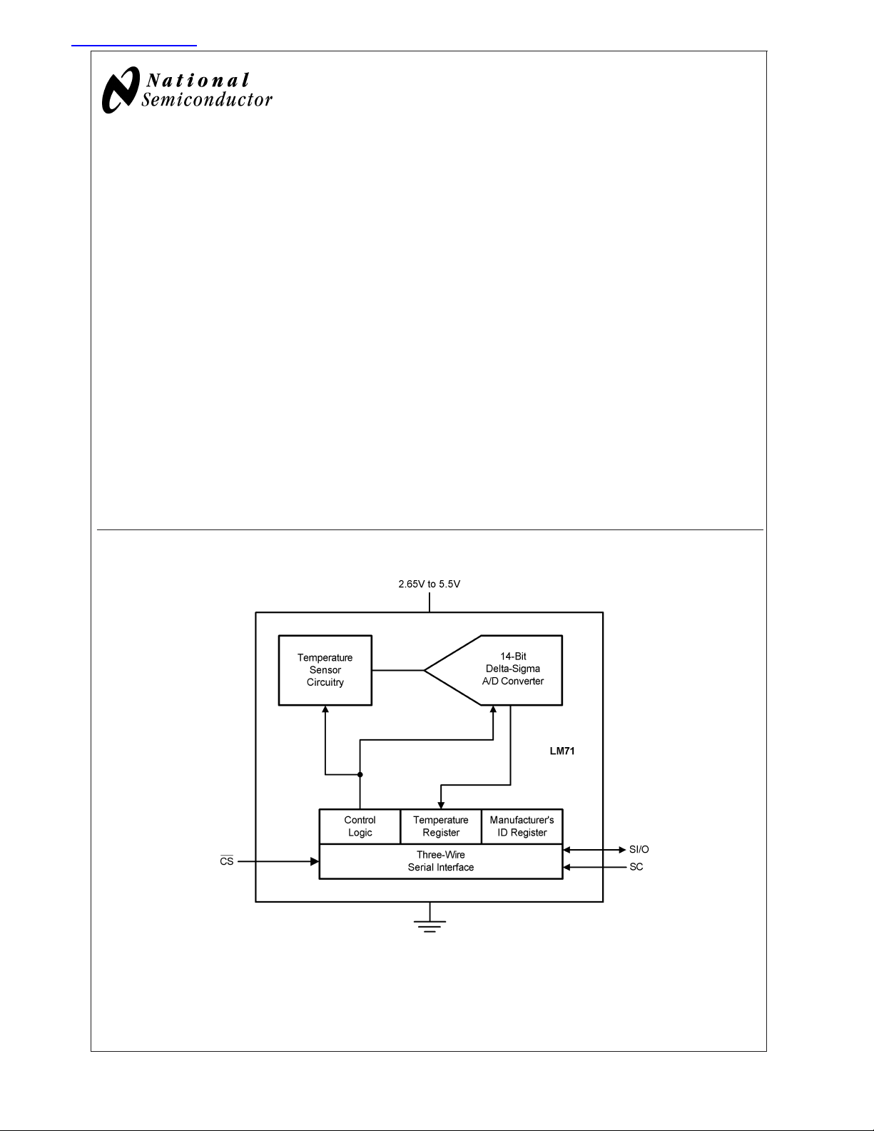
Simplified Block Diagram
n Electronic Test Equipment
n Vending Machines
Features
n SOT23-5 or No-Pull-Back LLP-6 Packages
n Operates over a full −40˚C to +150˚C range
n SPI and MICROWIRE Bus interface
Key Specifications
j
Supply Voltage 2.65V to 5.5V
j
Supply Current operating 300 µA (typ)
550 µA (max)
j
Temperature
±
Accuracy −10˚C to +65˚C
−40˚C to 150˚C +3/− 2˚C (max)
j
Temperature
Resolution
1.5˚C (max)
31.25 m˚C
20031701
MICROWIRE™is a trademark of National Semiconductor Corporation.
®
TRI-STATE
© 2004 National Semiconductor Corporation DS200317 www.national.com
is a registered trademark of National Semiconductor Corporation.
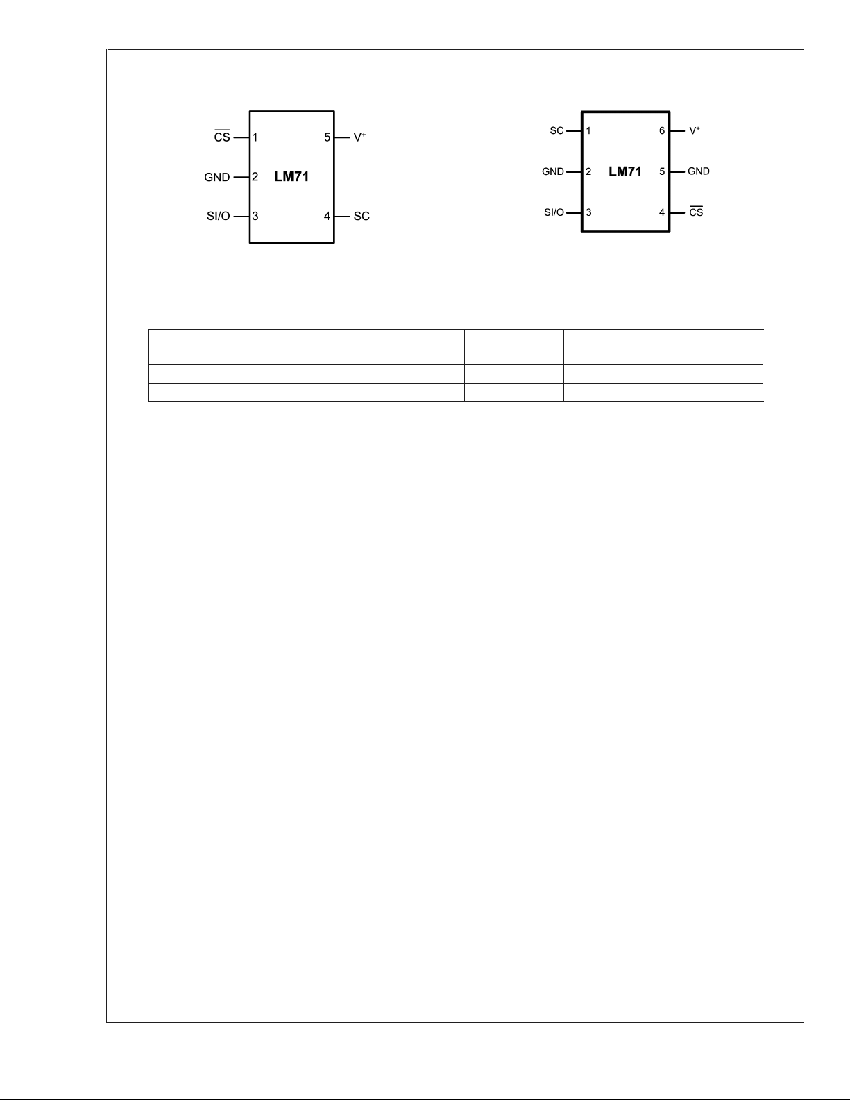
Connection Diagrams
LM71
SOT23-5 LLP-6 No Pull-Back
TOP VIEW
NS Package Number MF05A
Ordering Information
Order Number
LM71CIMF T16C MF05A 2.65V to 5.5V 3000 Units in Tape and Reel
LM71CISD LM71C SDE06A 2.65V to 5.5V 4500 Units in Tape and Reel
Package
Marking
20031702
NS Package
Number
TOP VIEW
20031728
NS Package Number SDE06A
Supply Voltage Transport Media
www.national.com 2
Pin Descriptions
Label Pin Number Function Typical Connection
SOT23-5 LLP-6
CS
GND 2 2, 5 Power Supply Ground Connect all GND Pins to ground
SI/O 3 3 Slave Input/Output - Serial bus
SC 4 1 Slave Clock - Serial bus clock Shmitt
+
V
1 4 Chip Select input From controller
From and to controller
bi-directional data line. Shmitt trigger input.
From controller
trigger input line
5 6 Positive Supply Voltage Input DC voltage from 2.65V to 5.5V. Bypass with a
0.1 µF ceramic capacitor.
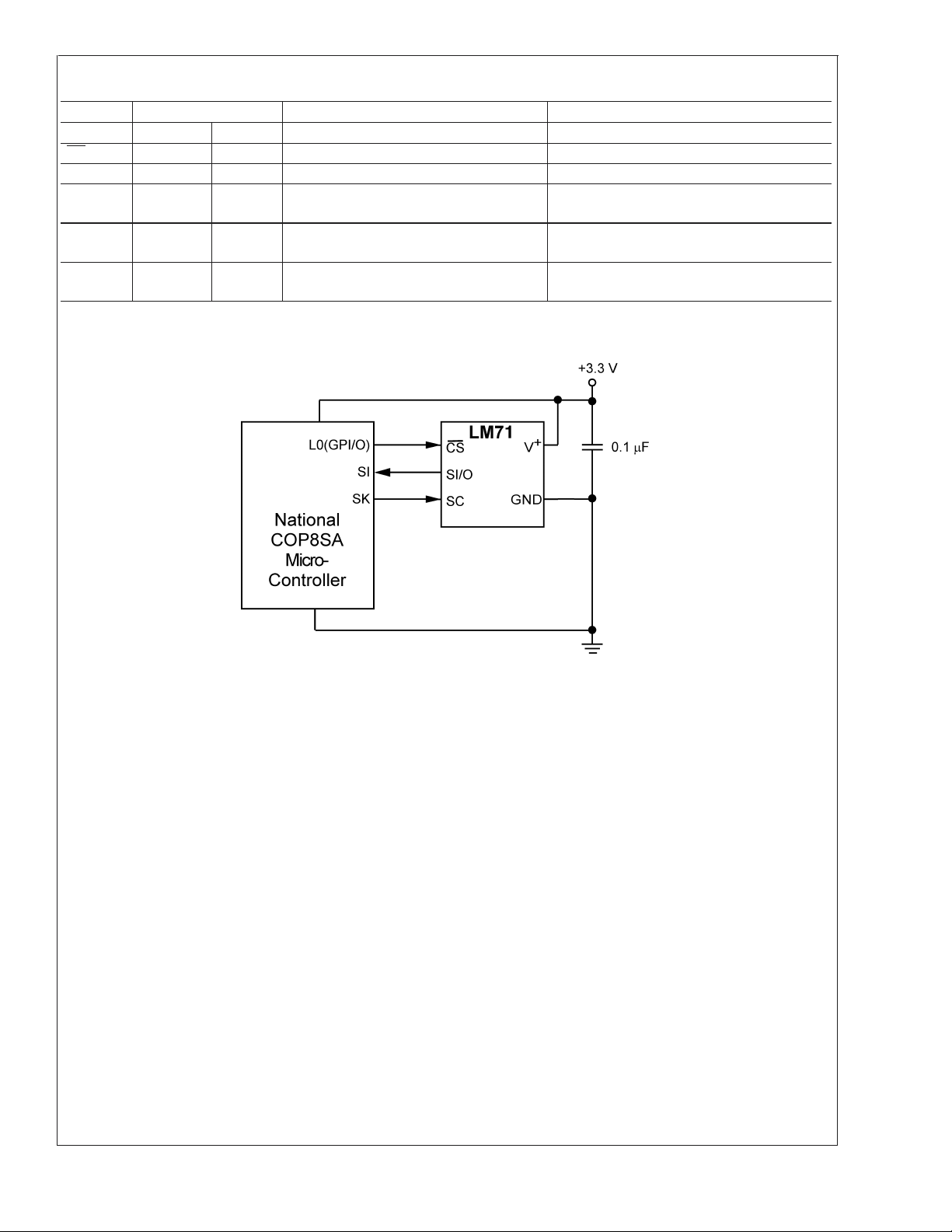
Typical Application
LM71
FIGURE 1. COP Microcontroller Interface
20031703
www.national.com3
Absolute Maximum Ratings (Note 1)
LM71
Supply Voltage −0.3V to 6.0V
Voltage at any Pin −0.3V to V
Input Current at any Pin (Note 2) 5 mA
Storage Temperature −65˚C to +150˚C
Soldering Information, Lead Temperature
SOT23-5 Package (Note 3)
Vapor Phase (60 seconds)
Infrared (15 seconds)
LLP-6 Package (Note 3)
Infrared (5 seconds) 215˚C
+
+ 0.3V
215˚C
220˚C
ESD Susceptibility (Note 4)
Human Body Model
Machine Model
Operating Ratings
Specified Temperature Range
(Note 5) T
LM71CIMF, LM71CISD −40˚C to +150˚C
Supply Voltage Range (+V
)
S
LM71CIMF, LM71CISD +2.65V to +5.5V
MIN
2000V
200V
to T
MAX
Temperature-to-Digital Converter Characteristics Unless otherwise noted, these specifica-
tions apply for V
+
= 2.65V to 3.6V (Note 6). Boldface limits apply for TA=TJ=T
MIN
to T
; all other limits TA=TJ=
MAX
+25˚C, unless otherwise noted.
LM71CIMF
Parameter Conditions
Typical
(Note 7)
LM71CISD
Limits
Units
(Limit)
(Note 8)
Temperature Error
= −10˚C to +65˚C
T
A
±
1.5 ˚C (max)
(Note 6)
TA= −40˚C to +85˚C
T
= −40˚C to +150˚C +3/−2 ˚C (max)
A
Resolution 14
0.03125
Temperature
(Note 9) 200 270 ms (max)
±
2.0 ˚C (max)
Bits
˚C
Conversion Time
Quiescent Current Serial Bus Inactive 300 550 µA (max)
Logic Electrical Characteristics
DIGITAL DC CHARACTERISTICS Unless otherwise noted, these specifications apply for V+= 2.65V to 3.6V (Note 6). Boldface limits apply for T
A=TJ=TMIN
to T
Symbol Parameter Conditions
V
IN(1)
V
IN(0)
Logical “1” Input Voltage V+x 0.7 V (min)
Logical “0” Input Voltage −0.3 V (min)
Input Hysteresis Voltage V
I
IN(1)
I
IN(0)
C
IN
V
OH
V
OL
I
O_TRI-STATE
Logical “1” Input Current VIN=V
Logical “0” Input Current VIN= 0V −0.005 −3.0 µA (min)
All Digital Inputs 20 pF
High Level Output Voltage IOH= −400 µA 2.4 V (min)
Low Level Output Voltage IOL=+2mA 0.4 V (max)
TRI-STATE®Output Leakage
Current
; all other limits TA=TJ= +25˚C, unless otherwise noted.
MAX
Typical
(Note 7)
+
= 3.0V to 3.6V 0.4 0.33 V (min)
+
0.005 3.0 µA (max)
VO= GND
+
=V
V
O
Limits
(Note 8)
+
V
+ 0.3 V (max)
+
V
x 0.3 V (max)
−1
+1
µA (max)
Units
(Limit)
µA (min)
www.national.com 4

Logic Electrical Characteristics (Continued)
SERIAL BUS DIGITAL SWITCHING CHARACTERISTICS Unless otherwise noted, these specifications apply for V+= 2.65V
to 3.6V (Note 6); C
=T
to T
MIN
MAX
Symbol Parameter Conditions
t
1
t
2
t
3
t
4
t
5
t
6
t
7
SC (Clock) Period 0.16
CS Low to SC (Clock) High Set-Up Time 100 ns (min)
CS Low to Data Out (SO) Delay 70 ns (max)
SC (Clock) Low to Data Out (SO) Delay 70 ns (max)
CS High to Data Out (SO) TRI-STATE 200 ns (max)
SC (Clock) High to Data In (SI) Hold Time 50 ns (min)
Data In (SI) Set-Up Time to SC (Clock) High 30 ns (min)
(load capacitance) on output lines = 100 pF unless otherwise specified. Boldface limits apply for TA=T
L
; all other limits TA=TJ= +25˚C, unless otherwise noted.
Typical
(Note 7)
Limits
(Note 8)
DC
Units
(Limit)
µs (min)
(max)
LM71
J
FIGURE 2. Data Output Timing Diagram
FIGURE 3. TRI-STATE Data Output Timing Diagram
20031704
20031705
www.national.com5

Logic Electrical Characteristics (Continued)
LM71
20031706
FIGURE 4. Data Input Timing Diagram
Note 1: Absolute Maximum Ratings indicate limits beyond which damage to the device may occur. DC and AC electrical specifications do not apply when operating
the device beyond its rated operating conditions.
Note 2: When the input voltage (V
Note 3: See AN-450 “Surface Mounting Methods and Their Effect on Product Reliability” or the section titled “Surface Mount” found in a current National
Semiconductor Linear Data Book for other methods of soldering surface mount devices.
Note 4: Human body model, 100 pF discharged through a 1.5 kΩ resistor. Machine model, 200 pF discharged directly into each pin.
Note 5: The life expectancy of the LM71 will be reduced when operating at elevated temperatures. LM71 θ
attached to a printed circuit board with 2 oz. foil is summarized in the table below:
) at any pin exceeds the power supplies (V
I
Device Number
<
GND or V
I
NS Package
Number
>
+VS) the current at that pin should be limited to 5 mA.
I
(thermal resistance, junction-to-ambient) when
JA
Thermal
Resistance (θ
)
JA
LM71CIMF MF05A 250˚C/W
LM71CISD SDE06A 57.6˚C/W
Note 6: The LM71 will operate properly over the V+supply voltage range of 2.65V to 5.5V.
Note 7: Typicals are at T
Note 8: Limits are guaranteed to National’s AOQL (Average Outgoing Quality Level).
Note 9: This specification is provided only to indicate how often temperature data is updated. The LM71 can be read at any time without regard to conversion state
(and will yield last conversion result). A conversion in progress will not be interrupted. The output shift register will be updated at the completion of the read and a
new conversion restarted.
Note 10: For best accuracy, minimize output loading. Higher sink currents can affect sensor accuracy with internal heating. This can cause an error of 0.64˚C at full
rated sink current and saturation voltage based on junction-to-ambient thermal resistance.
= 25˚C and represent most likely parametric norm.
A
www.national.com 6

Electrical Characteristics
LM71
20031708
FIGURE 5. Temperature-to-Digital Transfer Function (Non-linear scale for clarity)
TRI-STATE Test Circuit
20031707
FIGURE 6.
www.national.com7

Typical Performance Characteristics
LM71
Static Supply Current vs. Temperature Temperature Error
20031796 20031797
1.0 Functional Description
The LM71 temperature sensor incorporates a temperature
sensor and 13-bit plus sign ∆Σ ADC (Delta-Sigma Analog-toDigital Converter). Compatibility of the LM71’s three wire
serial interface with SPI and MICROWIRE allows simple
communications with common microcontrollers and processors. Shutdown mode can be used to optimize current drain
for different applications. A Manufacture’s/Device ID register
identifies the LM71 as National Semiconductor product.
1.1 POWER UP AND POWER DOWN
The LM71 always powers up in a known state. The power up
default condition is continuous conversion mode. Immediately after power up the LM71 will output an erroneous code
until the first temperature conversion has completed.
When the supply voltage is less than about 1.6V (typical),
the LM71 is considered powered down. As the supply voltage rises above the nominal 1.6V power up threshold, the
internal registers are reset to the power up default state
described above.
1.2 SERIAL BUS INTERFACE
The LM71 operates as a slave and is compatible with SPI or
MICROWIRE bus specifications. Data is clocked out on the
falling edge of the serial clock (SC), while data is clocked in
on the rising edge of SC. A complete transmit/receive communication will consist of 32 serial clocks. The first 16 clocks
comprise the transmit phase of communication, while the
second 16 clocks are the receive phase.
When CS is high SI/O will be in TRI-STATE. Communication
should be initiated by taking chip select (CS) low. This
should not be done when SC is changing from a low to high
state. Once CS is low the serial I/O pin (SI/O) will transmit
the first bit of data. The master can then read this bit with the
rising edge of SC. The remainder of the data will be clocked
out by the falling edge of SC. CS can be taken high at any
time during the transmit phase. If CS is brought low in the
middle of a conversion the LM71 will complete the conversion and the output shift register will be updated after CS is
brought back high.
The receive phase of a communication starts after 16 SC
periods. CS can remain low for 32 SC cycles. The LM71 will
read the data available on the SI/O line on the rising edge of
the serial clock. Input data is to an 8-bit shift register. The
part will detect the last eight bits shifted into the register. The
receive phase can last up to 16 SC periods. All ones must be
shifted in order to place the part into shutdown. All zeros
must be shifted in order to place the LM71 into continuous
conversion mode. Only the following codes should be transmitted to the LM71:
00 hex for continuous conversion
•
FF hex for shutdown
•
Another code may place the part into a test mode. Test
modes are used by National Semiconductor to thoroughly
test the function of the LM71 during production testing. Only
eight bits have been defined above since only the last eight
transmitted are detected by the LM71, before CS is taken
HIGH.
The following communication can be used to determine the
Manufacturer’s/Device ID and then immediately place the
part into continuous conversion mode. With CS continuously
low:
Read 16 bits of temperature data
•
Write 16 bits of data commanding shutdown
•
Read 16 bits of Manufacture’s/Device ID data
•
Write 8 to 16 bits of data commanding Conversion Mode
•
Take CS HIGH.
•
Note that 300 ms will have to pass for a conversion to
complete before the LM71 actually transmits temperature
data.
www.national.com 8

1.0 Functional Description (Continued)
1.3 TEMPERATURE DATA FORMAT
Temperature data is represented by a 14-bit, two’s complement word with an LSB (Least Significant Bit) equal to
0.03125˚C:
Temperature
+150˚C 0100 1011 0000 0011 4B03
+125˚C 0011 1110 1000 0011 3E83
+25˚C 0000 1100 1000 0011 0C83
+0.03125˚C 0000 0000 0000 0111 0007
0˚C 0000 0000 0000 0011 0003
−0.03125˚C 1111 1111 1111 1111 FFFF
−25˚C 1111 0 011 1000 0011 F383
−40˚C 1110 1100 0000 0011 EC03
The first data byte is the most significant byte with most
significant bit first, permitting only as much data as neces-
1.5.1 Configuration Register
(Selects shutdown or continuous conversion modes):
(Write Only):
D15 D14 D13 D12 D11 D10 D9 D8 D7 D6 D5 D4 D3 D2 D1 D0
XXXXXXXX Shutdown
Digital Output
Binary Hex
sary to be read to determine temperature condition. For
instance, if the first four bits of the temperature data indicate
an overtemperature condition, the host processor could immediately take action to remedy the excessive temperatures.
1.4 SHUTDOWN MODE/MANUFACTURER’S ID
Shutdown mode is enabled by writing XX FF to the LM71 as
shown in Figure 7c. The serial bus is still active when the
LM71 is in shutdown. When in shutdown mode the LM71
always will output 1000 0000 0000 1111. This is the
manufacturer’s/Device ID information. The first 5-bits of the
field (1000 0XXX) are reserved for manufacturer’s ID.
1.5 INTERNAL REGISTER STRUCTURE
The LM71 has three registers, the temperature register, the
configuration register and the manufacturer’s/device identification register. The temperature and manufacturer’s/device
identification registers are read only. The configuration register is write only.
LM71
D0–D15 set to XX FF hex enables shutdown mode.
D0–D15 set to 00 00 hex sets Continuous conversion mode.
Note: setting D0-D15 to any other values may place the LM70 into a manufacturer’s test mode, upon which the LM71 will stop
responding as described. These test modes are to be used for National Semiconductor production testing only. See Section 1.2
Serial Bus Interface for a complete discussion.
1.5.2 Temperature Register
(Read Only):
D15 D14 D13 D12 D11 D10 D9 D8 D7 D6 D5 D4 D3 D2 D1 D0
MSB Bit 12 Bit 11 Bit 10 Bit 9 Bit 8 Bit 7 Bit 6 Bit 5 Bit 4 Bit 3 Bit 2 Bit1 LSB 1 1
D0–D1: Logic 1 will be output on SI/0.
D2–D15: Temperature Data. One LSB = 0.03125˚C. Two’s complement format.
1.5.3 Manufacturer/Device ID Register
(Read Only):
D15 D14 D13 D12 D11 D10 D9 D8 D7 D6 D5 D4 D3 D2 D1 D0
1000000000001111
D0–D1: Logic 1 will be output on SI/0.
D2–D15: Manufacturer’s/Device ID Data. This register is accessed whenever the LM71 is in shutdown mode.
www.national.com9
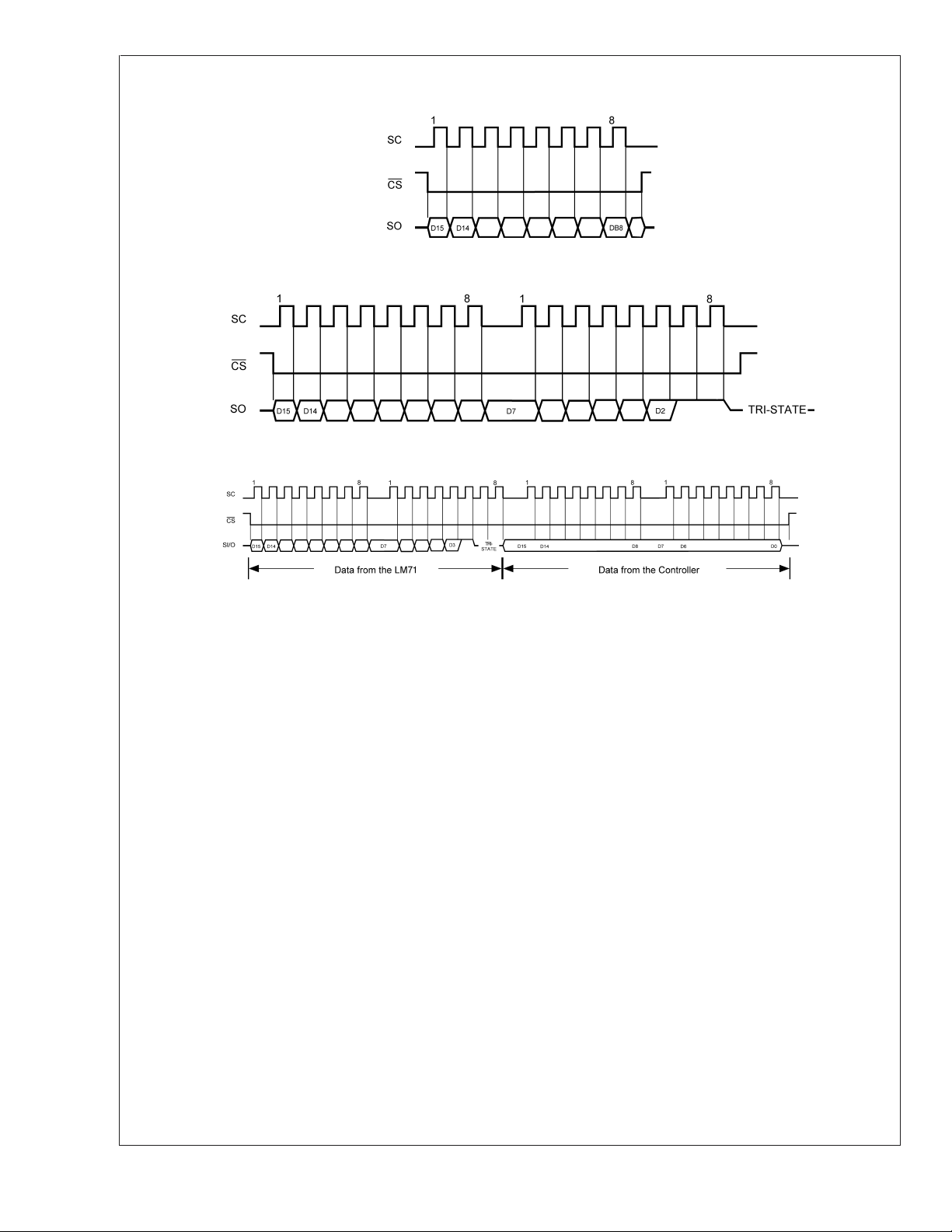
2.0 Serial Bus Timing Diagrams
LM71
a) Reading Continuous Conversion - Single Eight-Bit Frame
b) Reading Continuous Conversion - Two Eight-Bit Frames
c) Writing Shutdown Control
FIGURE 7. Timing Diagrams
3.0 Application Hints
To get the expected results when measuring temperature
with an integrated circuit temperature sensor like the LM71,
it is important to understand that the sensor measures its
own die temperature. For the LM71, the best thermal path
between the die and the outside world is through the LM71’s
pins. In the SOT23 package, all the pins on the LM71 will
have an equal effect on the die temperature. Because the
pins represent a good thermal path to the LM71 die, the
LM71 will provide an accurate measurement of the temperature of the printed circuit board on which it is mounted. There
is a less efficient thermal path between the plastic package
and the LM71 die. If the ambient air temperature is signifi-
20031714
20031715
20031718
cantly different from the printed circuit board temperature, it
will have a small effect on the measured temperature.
In probe-type applications, the LM71 can be mounted inside
a sealed-end metal tube, and can then be dipped into a bath
or screwed into a threaded hole in a tank. As with any IC, the
LM71 and accompanying wiring and circuits must be kept
insulated and dry, to avoid leakage and corrosion. This is
especially true if the circuit may operate at cold temperatures
where condensation can occur. Printed-circuit coatings and
varnishes such as Humiseal and epoxy paints or dips are
often used to insure that moisture cannot corrode the LM71
or its connections.
www.national.com 10

4.0 Typical Applications
LM71
20031720
FIGURE 8. Temperature monitor using Intel 196 processor
20031719
FIGURE 9. LM71 digital input control using micro-controller’s general purpose I/O.
www.national.com11

Physical Dimensions inches (millimeters) unless otherwise noted
LM71
Order Number LM71Top View
CIMF
NS Package Number MF05A
www.national.com 12

Physical Dimensions inches (millimeters) unless otherwise noted (Continued)
LM71 SPI/MICROWIRE 13-Bit Plus Sign Temperature Sensor
Order Number LM71Bottom View
CISD
NS Package Number SDE06A
LIFE SUPPORT POLICY
NATIONAL’S PRODUCTS ARE NOT AUTHORIZED FOR USE AS CRITICAL COMPONENTS IN LIFE SUPPORT
DEVICES OR SYSTEMS WITHOUT THE EXPRESS WRITTEN APPROVAL OF THE PRESIDENT AND GENERAL
COUNSEL OF NATIONAL SEMICONDUCTOR CORPORATION. As used herein:
1. Life support devices or systems are devices or
systems which, (a) are intended for surgical implant
into the body, or (b) support or sustain life, and
whose failure to perform when properly used in
accordance with instructions for use provided in the
2. A critical component is any component of a life
support device or system whose failure to perform
can be reasonably expected to cause the failure of
the life support device or system, or to affect its
safety or effectiveness.
labeling, can be reasonably expected to result in a
significant injury to the user.
BANNED SUBSTANCE COMPLIANCE
National Semiconductor certifies that the products and packing materials meet the provisions of the Customer Products
Stewardship Specification (CSP-9-111C2) and the Banned Substances and Materials of Interest Specification
(CSP-9-111S2) and contain no ‘‘Banned Substances’’ as defined in CSP-9-111S2.
National Semiconductor
Americas Customer
Support Center
Email: new.feedback@nsc.com
Tel: 1-800-272-9959
www.national.com
National does not assume any responsibility for use of any circuitry described, no circuit patent licenses are implied and National reserves the right at any time without notice to change said circuitry and specifications.
National Semiconductor
Europe Customer Support Center
Fax: +49 (0) 180-530 85 86
Email: europe.support@nsc.com
Deutsch Tel: +49 (0) 69 9508 6208
English Tel: +44 (0) 870 24 0 2171
Français Tel: +33 (0) 1 41 91 8790
National Semiconductor
Asia Pacific Customer
Support Center
Email: ap.support@nsc.com
National Semiconductor
Japan Customer Support Center
Fax: 81-3-5639-7507
Email: jpn.feedback@nsc.com
Tel: 81-3-5639-7560
 Loading...