

查询LM709供应商
LM709
Operational Amplifier
General Description
The LM709 series is a monolithic operational amplifier intended for general-purpose applications. Operation is completely specified over the range of voltages commonly used
for these devices. The design, in addition to providing high
gain, minimizes both offset voltage and bias currents. Further, the class-B output stage gives a large output capability
with minimum power drain.
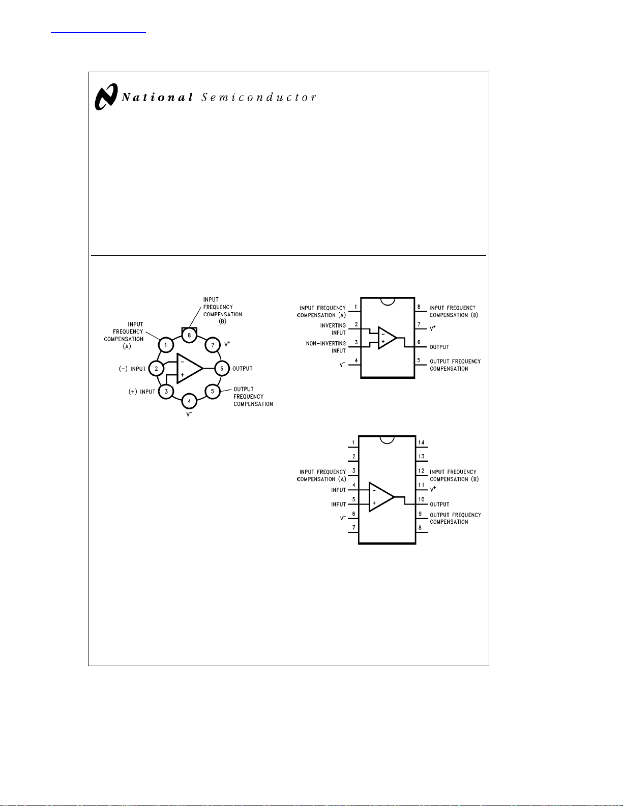
Connection Diagrams
Metal Can Package
February 1995
External components are used to frequency compensate
the amplifier. Although the unity-gain compensation network
specified will make the amplifier unconditionally stable in all
feedback configurations, compensation can be tailored to
optimize high-frequency performance for any gain setting.
The LM709C is the commercial-industrial version of the
LM709. It is identical to the LM709 except that it is specified
for operation from 0
Ctoa70§C.
§
Dual-In-Line Package
LM709 Operational Amplifier
TL/H/11477– 6
Order Number LM709CN-8
See NS Package Number N08E
TL/H/11477– 4
Order Number LM709AH, LM709H or LM709CH
See NS Package Number H08C
C
1995 National Semiconductor Corporation RRD-B30M115/Printed in U. S. A.
TL/H/11477
Dual-In-Line Package
TL/H/11477– 5
Order Number LM709CN
See NS Package Number N14A
Absolute Maximum Ratings (Note 3)
If Military/Aerospace specified devices are required,
please contact the National Semiconductor Sales
Office/Distributors for availability and specifications.
Supply Voltage
LM709/LM709A/LM709C
g
18V
Power Dissipation (Note 1)
LM709/LM709A 300 mW
LM709C 250 mW
Differential Input Voltage
LM709/LM709A/LM709C
g
5V
Input Voltage
LM709/LM709A/LM709C
Output Short-Circuit Duration (T
LM709/LM709A/LM709C 5 seconds
A
ea
25§C)
g
10V
Storage Temperature Range
LM709/LM709A/LM709C
b
65§Ctoa150§C
Lead Temperature (Soldering, 10 sec.)
LM709/LM709A/LM709C 300
Operating Ratings (Note 3)
Junction Temperature Range (Note 1)
LM709/LM709A
LM709C 0
Thermal Resistance (iJA)
H Package 150
8-Pin N Package 134
14-Pin N Package 109
b
55§Ctoa150§C
Ctoa100§C
§
C/W, (iJC)45§C/W
§
Electrical Characteristics (Note 2)
Parameter Conditions
s
25§C, R
10 kX 0.6 2.0 1.0 5.0 2.0 7.5 mV
S
25§C 100 200 200 500 300 1500 nA
25§C 10 50 50 200 100 500 nA
25§C 350 700 150 400 50 250 kX
25§C 150 150 150 X
e
25§C, V
20 mV, C
25§C 1.5 0.3 1.0 0.3 1.0 ms
g
15V 2.5 3.6 2.6 5.5 2.6 6.6 mA
S
s
100 pF
L
25§C 0.25 0.25 0.25 V/ms
10 kX 3.0 6.0 10 mV
10V
e
25§CtoT
A
e
A
e
A
e
T
A
t
2kX
L
e
10 kX
L
e
2kX
L
25§CtoT
25§CtoT
25§CtoT
MAX
MIN
MAX
MIN
50X T
10 kX T
g
15V, R
e
g
g
15V, R
g
15V, R
g
15V
10 kX
10 kX
T
MAX
T
MIN
T
MIN
T
MIN
55§CsT
s
a
125§C for the LM709/LM709A and 0§CsT
A
b
V
T
A
A
A
A
A
A
IN
A
A
S
S
S
S
OUT
S
S
S
S
S
A
A
A
A
e
e
e
e
e
e
e
e
e
s
e
e
e
e
e
e
s
s
e
e
e
e
Input Offset Voltage T
Input Bias Current T
Input Offset Current T
Input Resistance T
Output Resistance T
Supply Current T
Transient Response V
Risetime T
Overshoot 30 10 30 10 30 %
Slew Rate T
Input Offset Voltage R
Average Temperature R
Coefficient of T
Input Offset Voltage R
Large Signal V
Voltage Gain V
Output Voltage Swing V
Input Voltage Range V
Common-Mode R
Rejection Ratio
Supply Voltage R
Rejection Ratio
Input Offset Current T
Input Bias Current T
Input Resistance T
Note 1: For operating at elevated temperatures, the device must be derated based on a 150§C maximum junction temperature for LM709/LM709A and 100§C
maximum for L709C. For operating at elevated temperatures, the device must be derated based on thermal resistance i
Note 2: These specifications apply for
s
g
9VsV
Note 3: Absolute Maximum Ratings indicate limits which if exceeded may result in damage. Operating Ratings are conditions where the device is expected to be
functional but not necessarily within the guaranteed performance limits. For guaranteed specifications and test conditions, see the Electrical Characteristics.
g
15V, C1e5000 pF, R1e1.5 kX,C2e200 pF and R2e51X.
S
LM709A LM709 LM709C
Min Typ Max Min Typ Max Min Typ Max
1.8 10 3.0 6.0
1.8 10 6.0 12
2.0 15
4.8 25
25 70 25 45 70 15 45 V/mV
g12g
g10g
g
8
14
13
g12g
g10g
g8g
14
13
10
g12g
g10g
g8g
14
13
10 V
80 110 70 90 65 90 dB
40 100 25 150 25 200 mV/V
3.5 50 20 200 75 400
40 250 100 500 125 750
0.3 0.6 0.5 1.5 0.36 2.0 mA
85 170 40 100 50 250 kX
and TA.
s
a
A
JA,TJ(MAX)
70§C for the LM709C with the following conditions:
C/W
§
C/W
§
mV/
C
§
Units
V
nA
C
§
2
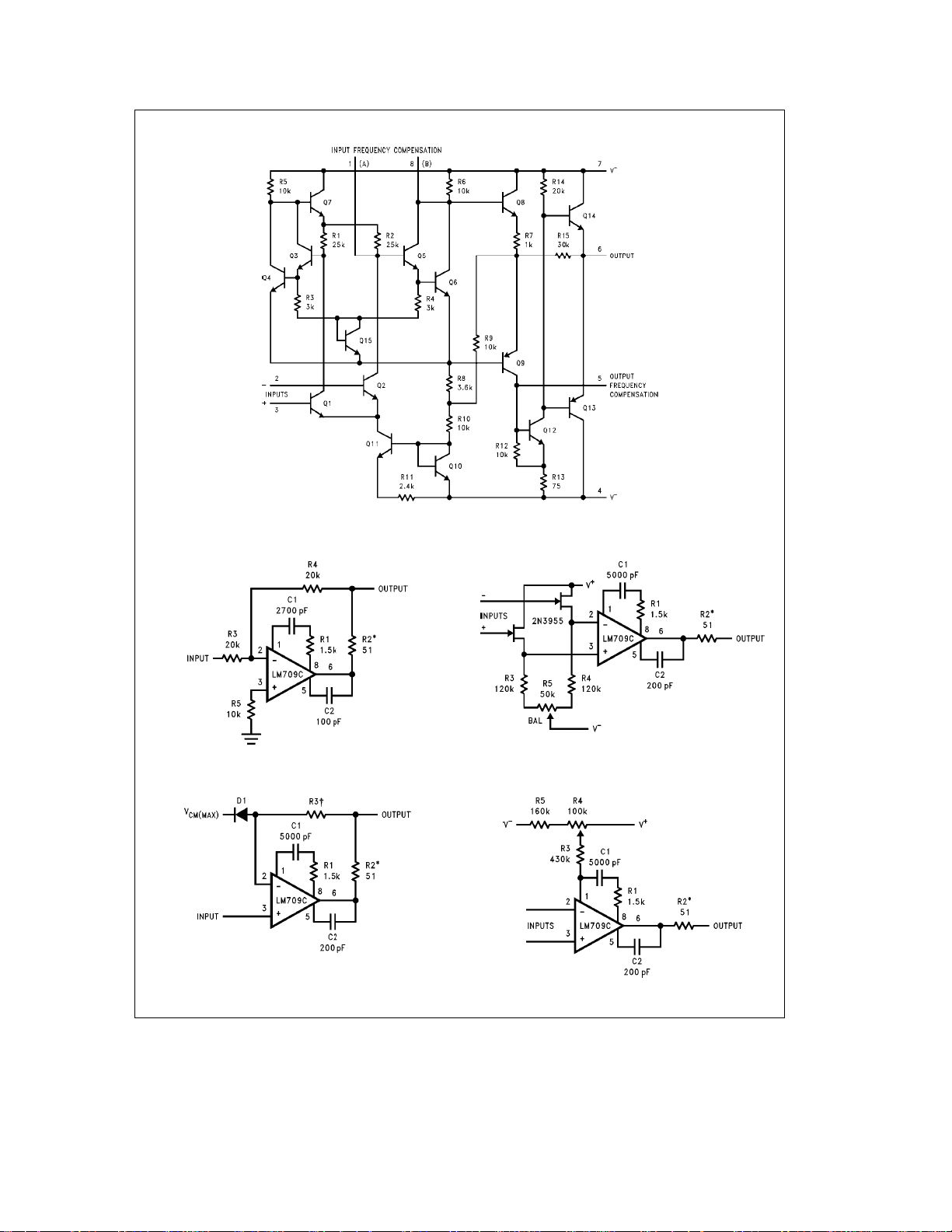
Schematic Diagram**
Typical Applications**
Unity Gain Inverting Amplifier
TL/H/11477– 1
FET Operational Amplifier
Voltage Follower
*To be used with any capacitive loading on output.
**Pin connections shown are for metal can package.
²
Should be equal to DC source resistance on input.
TL/H/11477– 2
TL/H/11477– 7
TL/H/11477– 3
Offset Balancing Circuit
TL/H/11477– 8
3
 Loading...