

LM6511
180 ns 3V Comparator
LM6511 180 ns 3V Comparator
March 2003
General Description
The LM6511 voltage comparator is ideal for analog-digital
interface circuitry when only a +3V or +3.3V supply is available. The open-collector output permits signal compatibility
with a wide variety of digital families: +5V CMOS, +3V
CMOS, TTL and so on. Supply voltage may range from 2.7V
to 36V between supply voltage leads. The LM6511 operates
with little power consumption (P
+2.7V and V
This voltage comparator offers many features that are available in traditional sub-microsecond comparators: output
sync strobe, inputs and output may be isolated from system
ground, and wire-ORing. Also, the LM6511 uses the
industry-standard, single comparator pinout configuration.
−
= 0V).
<
9.45 mW at V+=
diss
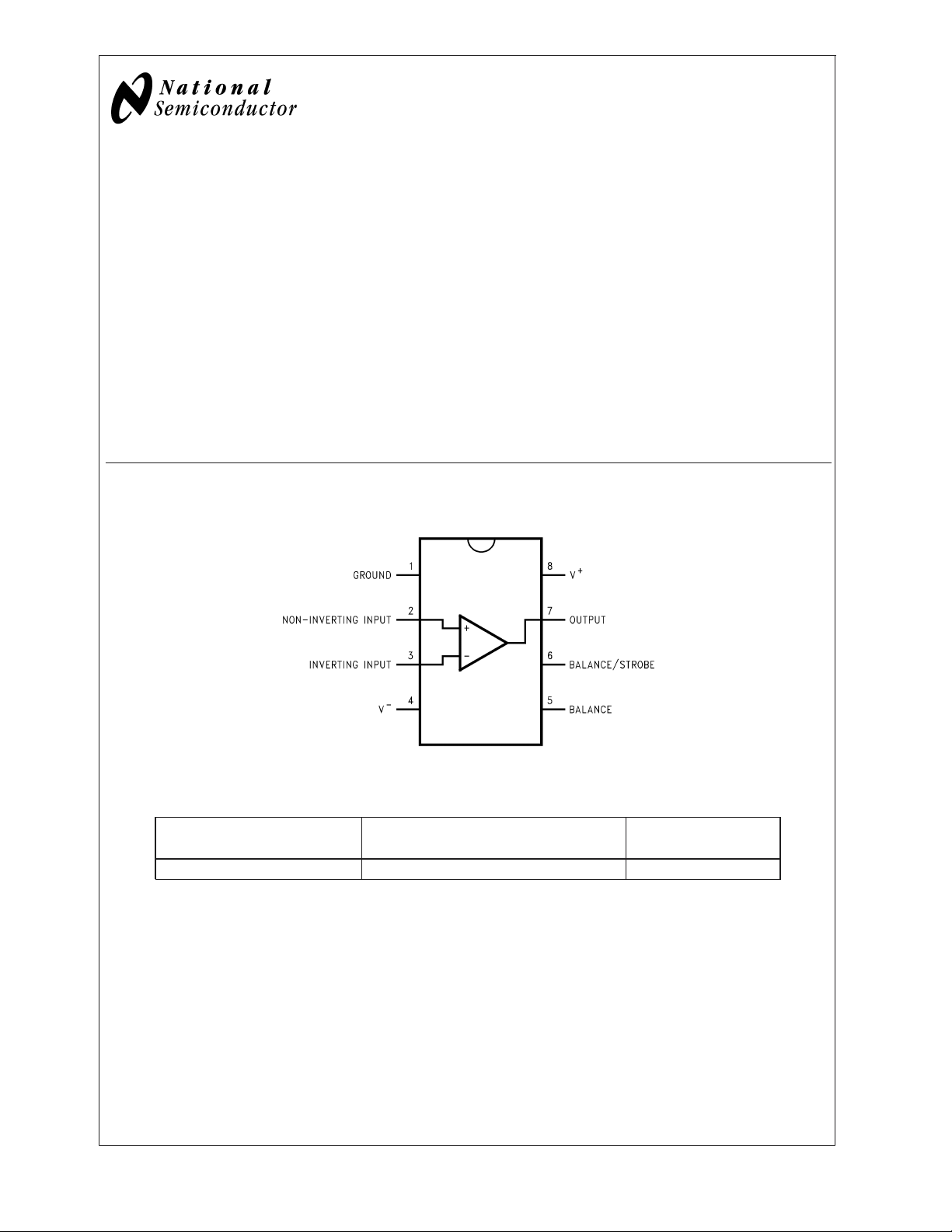
Connection Diagram
8-Pin SO
Features
(Typical unless otherwise noted)
n Operates at +2.7V, +3V, +3.3V, +5V
n Low Power consumption
n Fast Response Time of 180 ns
<
9.45 mW@V+= 2.7V (max)
Applications
n Portable Equipment
n Cellular Phones
n Digital Level Shifting
01188801
Ordering Information
Package Industrial Temperature Range NSC Package
−40˚C to +85˚C Drawing
8-Pin Small Outline LM6511IM, LM6511IMX M08A
© 2003 National Semiconductor Corporation DS011888 www.national.com
Absolute Maximum Ratings (Note 1)
If Military/Aerospace specified devices are required,
LM6511
please contact the National Semiconductor Sales Office/
Distributors for availability and specifications.
Supply Voltage −0.3 to +36V
Power Dissipation 500 mW
Output Short Circuit Duration 10s
Junction Temperature 150˚C
ESD Rating
(C = +100 pF, R = 1.5 kΩ) 300V
Output to Negative Supply Voltage 50V
Ground to Negative Supply Voltage 30V
±
Differential Input Voltage
30V
Input Voltage (Note 2)
Storage Temperature Range −65˚C to +150˚C
Operating Ratings (Note 1)
Supply Voltage 2.5V to 30V
Temperature Range −40˚C ≤ T
Soldering Information:
SO Package
(Vapor Phase in 60 sec)
SO Package (Infrared in 15 sec)
215˚C
220˚C
Thermal Resistance (θ
SO Package 170˚C/W
)
JA
DC Electrical Characteristics
Unless otherwise specified, all limits guaranteed for TJ= 25˚C. Boldface limits apply at the temperature extremes. V+= 2.7V,
−
= 0V, 50Ω≤RL≤ 50kΩ, and IL= 1.0 mA unless otherwise specified
V
Symbol Parameter Conditions Typical LM6511I Units
Limit
V
OS
I
B
I
OS
I
S
V
SAT
A
V
CMRR Common Mode Rejection Ratio 72 dB
I
STROBE
V
IN
Offset Voltage RS≤ 50 kΩ 1.5 5 mV
(Note 3) 8 max
Input Bias Current 38 130
200 nA
Input Offset Current RS≤ 50 kΩ 1.5 20
(Note 3) 50
Positive Supply Current 2.7 3.5
5 mA
Negative Supply Current 1.5 2.0
2.5
Saturation Voltage VIN≤ 10 mV 0.23 0.4 V
I
=8mA 0.4 max
SINK
Large Signal Voltage Gain ∆V
= 2V 40 V/mV
OUT
Strobe ON Current (Note 5) 2.0 5.0 mA max
Input Voltage Range 0.50 V min
+
V
− 1.25 V max
Output Leakage Current V
≥ 10 mV, V
IN
I
STROBE
= 35V, 0.2 nA
OUT
= 3 mA max
J
+85˚C
(Limits)
max
max
≤
AC Electrical Characteristics
Unless otherwise specified, all limits guaranteed for TJ= 25˚C. Boldface limits apply at the temperature extremes. V+= 2.7V,
−
= 0V, 50Ω≤RL≤ 50kΩ, and IL= 1.0 mA unless otherwise specified
V
Symbol Parameter Conditions Typical LM6511I Units
Limit
T
R
Note 1: Absolute Maximum Ratings indicate limits beyond which damage to the device may occur. Operating ratings indicate conditions the device is intended to
be functional, but do not guarantee specific performance limits. For guaranteed specifications and test conditions, see the Electrical Characteristics. The guaranteed
specifications apply only for the test conditions listed.
Note 2: The positive input voltage limit is 30V above the negative supply voltage. The negative input voltage limit is equal to the negative supply voltage or 30V
below the positive supply voltage, whichever is less.
Note 3: The offset voltage and offset current limits are the maximum values required to drive the output within a volt of either supply witha1mAload. Therefore,
these parameters define an error band and take into account the worst-case effects of voltage gain and input impedance.
Note 4: This specification is for a 100 mV input step with a 25 mV overdrive.
www.national.com 2
Response Time (Note 4) 180 ns
(Limits)

AC Electrical Characteristics (Continued)
Note 5: This specification gives the range of current which must be drawn from the strobe pin to ensure the output is properly disabled. Do not short the strobe pin
to ground; it should be current driven at 3 mA to 5 mA.
LM6511
LM6511 Typical Performance Characteristics V
Input Bias Current Input Offset Current
01188808
Input Current vs. Input Voltage Common Mode Limits
= 3V unless otherwise noted
S
01188809
01188810
Transfer Function Output Saturation Voltage
01188812
01188811
01188813
www.national.com3

LM6511 Typical Performance Characteristics V
LM6511
Output Current Limiting Supply Current vs. Temperature
= 3V unless otherwise noted (Continued)
S
Output Leakage Current Propagation Delay vs. Overdrive
Typical Application
01188814
01188816
Universal Logic Level Shifter
01188815
01188803
Notes: Because of the very wide operating and output voltage range, the LM6511 may be used to shift logic levels from 3V to TTL or CMOS to the other way
around. By biasing the input to
go to the output logic supply (V
1
⁄2of the input logic supply (VA), this assures that this input remains within the input voltage range. The pull-up resistor should
).
B
01188804
www.national.com 4
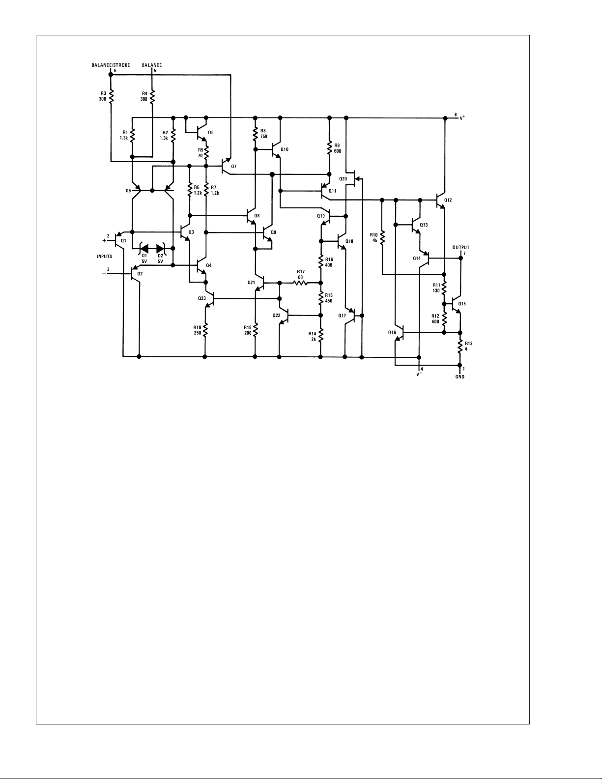
Schematic Diagram
LM6511
01188805
www.national.com5

Physical Dimensions inches (millimeters) unless otherwise noted
LM6511 180 ns 3V Comparator
8-Pin Small Outline Package (M)
Order Number LM6511IM, LM6511IMX
Package Number M08A
LIFE SUPPORT POLICY
NATIONAL’S PRODUCTS ARE NOT AUTHORIZED FOR USE AS CRITICAL COMPONENTS IN LIFE SUPPORT
DEVICES OR SYSTEMS WITHOUT THE EXPRESS WRITTEN APPROVAL OF THE PRESIDENT AND GENERAL
COUNSEL OF NATIONAL SEMICONDUCTOR CORPORATION. As used herein:
1. Life support devices or systems are devices or
systems which, (a) are intended for surgical implant
into the body, or (b) support or sustain life, and
whose failure to perform when properly used in
accordance with instructions for use provided in the
2. A critical component is any component of a life
support device or system whose failure to perform
can be reasonably expected to cause the failure of
the life support device or system, or to affect its
safety or effectiveness.
labeling, can be reasonably expected to result in a
significant injury to the user.
National Semiconductor
Americas Customer
Support Center
Email: new.feedback@nsc.com
Tel: 1-800-272-9959
www.national.com
National does not assume any responsibility for use of any circuitry described, no circuit patent licenses are implied and National reserves the right at any time without notice to change said circuitry and specifications.
National Semiconductor
Europe Customer Support Center
Fax: +49 (0) 180-530 85 86
Email: europe.support@nsc.com
Deutsch Tel: +49 (0) 69 9508 6208
English Tel: +44 (0) 870 24 0 2171
Français Tel: +33 (0) 1 41 91 8790
National Semiconductor
Asia Pacific Customer
Support Center
Fax: +65-6250 4466
Email: ap.support@nsc.com
Tel: +65-6254 4466
National Semiconductor
Japan Customer Support Center
Fax: 81-3-5639-7507
Email: jpn.feedback@nsc.com
Tel: 81-3-5639-7560
 Loading...