


October 2003
LM5110
Dual 5A Compound Gate Driver with Negative Output
Voltage Capability
General Description
The LM5110 Dual Gate Driver replaces industry standard
gate drivers with improved peak output current and efficiency. Each “compound” output driver stage includes MOS
and bipolar transistors operating in parallel that together sink
more than 5A peak from capacitive loads. Combining the
unique characteristics of MOS and bipolar devices reduces
drive current variation with voltage and temperature. Separate input and output ground pins provide Negative Drive
Capability allowing the user to drive MOSFET gates with
positive and negative VGS voltages. The gate driver control
inputs are referenced to a dedicated input ground (IN_REF).
The gate driver outputs swing from V
which can be negative with respect to IN_REF. The
V
EE
ability to hold MOSFET gates off with a negative VGS voltage reduces losses when driving low threshold voltage
MOSFETs often used as synchronous rectifiers. When driving with conventional positive only gate voltage, the IN_REF
and V
common ground. Under-voltage lockout protection and a
shutdown input pin are also provided. The drivers can be
operated in parallel with inputs and outputs connected to
double the drive current capability. This device is available in
the SOIC-8 and the thermally-enhanced LLP-10 packages.
pins are connected together and referenced to a
EE
to the output ground
CC
Features
n Independently drives two N-Channel MOSFETs
n Compound CMOS and bipolar outputs reduce output
current variation
n 5A sink/3A source current capability
n Two channels can be connected in parallel to double the
drive current
n Independent inputs (TTL compatible)
n Fast propagation times (25 ns typical)
n Fast rise and fall times (14 ns/12 ns rise/fall with 2 nF
load)
n Dedicated input ground pin (IN_REF) for split supply or
single supply operation
n Outputs swing from V
relative to input ground
n Available in dual non-inverting, dual inverting and
combination configurations
n Shutdown input provides low power mode
n Supply rail under-voltage lockout protection
n Pin-out compatible with industry standard gate drivers
to VEEwhich can be negative
CC
Typical Applications
n Synchronous Rectifier Gate Drivers
n Switch-mode Power Supply Gate Driver
n Solenoid and Motor Drivers
n Power Level Shifter
Package
n SOIC-8
n LLP-10 (4 mmx4mm)
LM5110 Dual 5A Compound Gate Driver with Negative Output Voltage Capability
Ordering Information
Order Number Package Type NSC Package Drawing Supplied As
LM5110-1/2/3 M SOIC-8 M08A Shipped in anti-static units
LM5110-1/2/3 MX SOIC-8 M08A 2500 shipped in Tape & Reel
LM5110-1/2/3 SD LLP-10 SDC10A 1000 shipped in Tape & Reel
LM5110-1/2/3 SDX LLP-10 SDC10A 4500 shipped in Tape & Reel
© 2003 National Semiconductor Corporation DS200792 www.national.com

Pin Configurations
LM5110
Block Diagram
SOIC-8
20079201
LLP-10
20079202
NC - NOT CONNECTED
Block Diagram of LM5110
www.national.com 2
20079203

Typical Application
LM5110
Simplified Power Converter Using Synchronous Rectifiers
with Negative Off Gate Voltage
20079204
www.national.com3

Pin Description
LM5110
SOIC-8 LLP-10
Note: Pins 5 and 6 are No Connect for LLP-10 package.
Pin
Description
Name Description Application Information
1 1 IN_REF Ground reference for control
2 2 IN_A ‘A’ side control input TTL compatible thresholds.
33V
EE
4 4 IN_B ‘B’ side control input TTL compatible thresholds.
5 7 OUT_B Output for the ‘B’ side driver. Capable of sourcing 3A and sinking 5A. Voltage
68V
CC
7 9 OUT_A. Output for the ‘A’ side driver. Capable of sourcing 3A and sinking 5A. Voltage
8 10 nSHDN Shutdown input pin Pull below 1.5V to activate low power shutdown
Configuration Table
inputs
Connect to V
voltage swing. Connect to system logic ground
for standard positive only output
EE
reference for positive and negative output voltage
swing.
Power ground of the driver
outputs
Connect to either power ground or a negative gate
drive supply.
swing of this output is from V
CC
to VEE.
Positive supply Locally decouple to VEEand IN_REF.
swing of this output is from VCCto VEE.
mode.
Part Number “A” Output Configuration “B” Output Configuration Package
LM5110-1M Non-Inverting Non-Inverting SOIC- 8
LM5110-2M Inverting Inverting SOIC- 8
LM5110-3M Inverting Non-Inverting SOIC- 8
LM5110-1SD Non-Inverting Non-Inverting LLP-10
LM5110-2SD Inverting Inverting LLP-10
LM5110-3SD Inverting Non-Inverting LLP-10
www.national.com 4

LM5110
Absolute Maximum Ratings (Note 1)
If Military/Aerospace specified devices are required,
please contact the National Semiconductor Sales Office/
Distributors for availability and specifications.
to V
V
CC
EE
V
to IN_REF −0.3V to 15V
CC
−0.3V to 15V
IN_REF to V
Storage Temperature Range, (T
EE
) −55˚C to +150˚C
STG
Maximum Junction Temperature,
(max)) +150˚C
(T
J
Operating Junction Temperature +125˚C
ESD Rating 2kV
−0.3V to 5V
IN to IN_REF, nSHDN to IN_REF −0.3V to 15V
Electrical Characteristics
TJ= −40˚C to +125˚C, VCC= 12V, VEE= IN_REF = 0V, nSHDN = VCC, No Load on OUT_A or OUT_B, unless otherwise
specified.
Symbol Parameter Conditions Min Typ Max Units
Operating Range VCC−IN_REF and VCC−V
V
CC
V
CCR
VCCUnder Voltage Lockout
VCC−IN_REF
(rising)
V
CCH
VCCUnder Voltage Lockout
Hysteresis
I
CC
VCCSupply Current (ICC) IN_A = IN_B = 0V (5110-1) 1 2
IN_A = IN_B = V
CC
(5110-2)
IN_A = V
,IN_B=0V
CC
(5110-3)
I
CCSD
VCCShutdown Current (ICC) nSHDN = 0V 18 25 µA
CONTROL INPUTS
V
IH
V
IL
Logic High 1.75 2.2 V
Logic Low 0.8 1.35 V
HYS Input Hysteresis 400 mV
I
IL
Input Current Low IN_A=IN_B=V
CC
(5110-1-2-3)
I
IH
Input Current High IN_A=IN_B=VCC(5110-1) 10 18 25
IN_A=IN_B=V
IN_A=V
CC
IN_B=V
CC
(5110-2) −1 0.1 1
CC
(5110-3) -1 0.1 1
(5110-3) 10 18 25
SHUTDOWN INPUT
ISD Pull-up Current nSHDN=0V −18 −25 µA
VSDR Shutdown Threshold nSHDN rising 0.8 1.5 2.2 V
VSDH Shutdown Hysteresis 165 mV
OUTPUT DRIVERS
R
OH
R
OL
I
Source
Output Resistance High I
Output Resistance Low I
= −10 mA 30 50 Ω
OUT
= + 10 mA 1.4 2.5 Ω
OUT
Peak Source Current OUTA/OUTB = VCC/2,
200 ns Pulsed Current
I
Sink
Peak Sink Current OUTA/OUTB = VCC/2,
200 ns Pulsed Current
3.5 14 V
EE
2.3 2.9 3.5 V
230 mV
12
12
−1 0.1 1
3A
5A
mA
µA
www.national.com5

Electrical Characteristics (Continued)
TJ= −40˚C to +125˚C, VCC= 12V, VEE= IN_REF = 0V, nSHDN = VCC, No Load on OUT_A or OUT_B, unless otherwise
LM5110
specified.
Symbol Parameter Conditions Min Typ Max Units
SWITCHING CHARACTERISTICS
td1 Propagation Delay Time Low to
High, IN rising (IN to OUT)
td2 Propagation Delay Time High to
Low, IN falling (IN to OUT)
t
r
t
f
Rise Time C
Fall Time C
C
= 2 nF, see Figure
LOAD
1
= 2 nF, see Figure
C
LOAD
1
= 2.0 nF, see Figure
LOAD
1
= 2 nF, see Figure
LOAD
1
25 40 ns
25 40 ns
14 25 ns
12 25 ns
LATCHUP PROTECTION
AEC - Q100, Method 004 T
Note 1: Absolute Maximum Ratings are limits beyond which damage to the device may occur. Operating Ratings are conditions under which operation of the device
is intended to be functional. For guaranteed specifications and test conditions, see the Electrical Characteristics.
= 150˚C 500 mA
J
Timing Waveforms
(a)
20079205
FIGURE 1. (a) Inverting, (b) Non-Inverting
www.national.com 6
(b)
20079206

Typical Performance Characteristics
Supply Current vs Frequency Supply Current vs Capacitive Load
LM5110
20079210
Rise and Fall Time vs Supply Voltage Rise and Fall Time vs Temperature
20079212 20079213
Rise and Fall Time vs Capacitive Load Delay Time vs Supply Voltage
20079211
20079214
20079215
www.national.com7
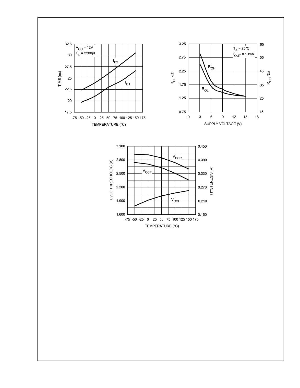
Typical Performance Characteristics (Continued)
LM5110
Delay Time vs Temperature RDSON vs Supply Voltage
20079216
UVLO Thresholds and Hysteresis vs Temperature
20079217
Detailed Operating Description
LM5110 dual gate driver consists of two independent and
identical driver channels with TTL compatible logic inputs
and high current totem-pole outputs that source or sink
current to drive MOSFET gates. The driver output consist of
a compound structure with MOS and bipolar transistor operating in parallel to optimize current capability over a wide
output voltage and operating temperature range. The bipolar
device provides high peak current at the critical threshold
region of the MOSFET VGS while the MOS devices provide
rail-to-rail output swing. The totem pole output drives the
MOSFET gate between the gate drive supply voltage V
and the power ground potential at the VEEpin.
The control inputs of the drivers are high impedance CMOS
buffers with TTL compatible threshold voltages. The negative supply of the input buffer is connected to the input
ground pin IN_REF. An internal level shifting circuit connects
the logic input buffers to the totem pole output drivers. The
level shift circuit and separate input/output ground pins provide the option of single supply or split supply configurations.
When driving MOSFET gates from a single positive supply,
the IN_REF and V
www.national.com 8
pins are both connected to the power
EE
CC
20079218
ground. The LM5110 pinout was designed for compatibility
with industry standard gate drivers in single supply gate
driver applications. Pin 1 (IN_REF) on the LM5110 is a
no-connect on standard driver IC’s. Connecting pin 1 to pin 3
(V
) on the printed circuit board accommodates the pin-out
EE
of both the LM5110 and competitive drivers.
The isolated input/output grounds provide the capability to
drive the MOSFET to a negative VGS voltage for a more
robust and reliable off state. In split supply configuration, the
IN_REF pin is connected to the ground of the controller
which drives the LM5110 inputs. The V
pin is connected to
EE
a negative bias supply that can range from the IN-REF as
much as 14V below the V
mum recommended voltage difference between V
IN_REF or between V
voltage difference between V
gate drive supply. The maxi-
CC
and VEEis 14V. The minimum
CC
and IN_REF is 3.5V.
CC
and
CC
Enhancement mode MOSFETs do not inherently require a
negative bias on the gate to turn off the FET. However,
certain applications may benefit from the capability of negative VGS voltage during turn-off including:
1. when the gate voltages cannot be held safely below the
threshold voltage due to transients or coupling in the
printed circuit board.

Detailed Operating Description
(Continued)
2. when driving low threshold MOSFETs at high junction
temperatures
3. when high switching speeds produce capacitive gatedrain current that lifts the internal gate potential of the
MOSFET
The two driver channels of the LM5110 are designed as
identical cells. Transistor matching inherent to integrated
circuit manufacturing ensures that the ac and dc performance of the channels are nearly identical. Closely matched
propagation delays allow the dual driver to be operated as a
single driver if inputs and output pins are connected. The
drive current capability in parallel operation is 2X the drive of
either channel. Small differences in switching speed between the driver channels will produce a transient current
(shoot-through) in the output stage when two output pins are
connected to drive a single load. The efficiency loss for
parallel operation has been characterized at various loads,
supply voltages and operating frequencies. The power dissipation in the LM5110 increases by less than 1% relative to
the dual driver configuration when operated as a single
driver with inputs and outputs connected.
An Under-voltage lockout (UVLO) circuit is included in the
LM5110, which senses the voltage difference between V
CC
and the input ground pin, IN_REF. When the VCCto IN_REF
voltage difference falls below 2.7V both driver channels are
disabled. The driver will resume normal operation when the
to IN_REF differential voltage exceeds approximately
V
CC
2.9V. UVLO hysteresis prevents chattering during brown-out
conditions.
The Shutdown pin (nSHDN) is a TTL compatible logic input
provided to enable/disable both driver channels. When
nSHDN is in the logic low state, the LM5110 is switched to a
low power standby mode with total supply current less than
25 µA. This function can be effectively used for start-up,
thermal overload, or short circuit fault protection. It is recommended that this pin be connected to V
when the shut-
CC
down function is not being used. The shutdown pin has an
internal 18µA current source pull-up to V
.
CC
The input pins of non-inverting drivers have an internal 18µA
current source pull-down to IN-REF. The input pins of inverting driver channels have neither pull-up nor pull-down current sources.
The LM5110 is available in dual non-inverting (-1), dual
inverting (-2) and the combination inverting plus noninverting (-3) configurations. All three configurations are offered in the SOIC-8 and LLP-10 plastic packages.
Layout Considerations
Attention must be given to board layout when using LM5110.
Some important considerations include:
1. A Low ESR/ESL capacitor must be connected close to
the IC and between the V
and VEEpins to support
CC
high peak currents being drawn from V
during turn-on
CC
of the MOSFET.
2. Proper grounding is crucial. The drivers need a very low
impedance path for current return to ground avoiding
inductive loops. The two paths for returning current to
ground are a) between LM5110 IN-REF pin and the
ground of the circuit that controls the driver inputs, b)
between LM5110 V
pin and the source of the power
EE
MOSFET being driven. All these paths should be as
short as possible to reduce inductance and be as wide
as possible to reduce resistance. All these ground paths
should be kept distinctly separate to avoid coupling between the high current output paths and the logic signals
that drive the LM5110. A good method is to dedicate one
copper plane in a multi-layered PCB to provide a common ground surface.
3. With the rise and fall times in the range of 10 ns to 30 ns,
care is required to minimize the lengths of current carrying conductors to reduce their inductance and EMI
from the high di/dt transients generated by the LM5110.
4. The LM5110 SOIC footprint is compatible with other
industry standard drivers. Simply connect IN_REF pin of
the LM5110 to V
(pin 1 to pin 3) to operate the LM5110
EE
in a standard single supply configuration.
5. If either channel is not being used, the respective input
pin (IN_A or IN_B) should be connected to either
IN_REF or V
to avoid spurious output signals. If the
CC
shutdown feature is not used, the nSHDN pin should be
connected to V
to avoid erratic behavior that would
CC
result if system noise were coupled into a floating
’nSHDN’ pin.
Thermal Performance
INTRODUCTION
The primary goal of thermal management is to maintain the
integrated circuit (IC) junction temperature (T
specified maximum operating temperature to ensure reliability. It is essential to estimate the maximum T
nents in worst case operating conditions. The junction temperature is estimated based on the power dissipated in the
IC and the junction to ambient thermal resistance θ
IC package in the application board and environment. The
is not a given constant for the package and depends on
θ
JA
the printed circuit board design and the operating environment.
DRIVE POWER REQUIREMENT CALCULATIONS IN LM5110
The LM5110 dual low side MOSFET driver is capable of
sourcing/sinking 3A/5A peak currents for short intervals to
drive a MOSFET without exceeding package power dissipation limits. High peak currents are required to switch the
MOSFET gate very quickly for operation at high frequencies.
) below a
J
of IC compo-
J
for the
JA
LM5110
www.national.com9

Thermal Performance (Continued)
LM5110
20079207
FIGURE 2.
The schematic above shows a conceptual diagram of the
LM5110 output and MOSFET load. Q1 and Q2 are the
switches within the gate driver. R
the external MOSFET, and C
is the gate resistance of
G
is the equivalent gate capaci-
IN
tance of the MOSFET. The gate resistance Rg is usually very
small and losses in it can be neglected. The equivalent gate
capacitance is a difficult parameter to measure since it is the
combination of C
(gate to source capacitance) and C
GS
GD
(gate to drain capacitance). Both of these MOSFET capacitances are not constants and vary with the gate and drain
voltage. The better way of quantifying gate capacitance is
the total gate charge Q
charge required by C
voltage V
GATE
.
in coloumbs. QGcombines the
G
and CGDfor a given gate drive
GS
Assuming negligible gate resistance, the total power dissipated in the MOSFET driver due to gate charge is approximated by
DRIVER
=V
GATExQGxFSW
P
Where
= switching frequency of the MOSFET.
F
SW
As an example, consider the MOSFET MTD6N15 whose
gate charge specified as 30 nC for V
GATE
= 12V.
The power dissipation in the driver due to charging and
discharging of MOSFET gate capacitances at switching frequency of 300 kHz and V
P
= 12V x 30 nC x 300 kHz = 0.108W.
DRIVER
of 12V is equal to
GATE
If both channels of the LM5110 are operating at equal frequency with equivalent loads, the total losses will be twice as
this value which is 0.216W.
In addition to the above gate charge power dissipation, transient power is dissipated in the driver during output
transitions. When either output of the LM5110 changes state,
current will flow from V
to VEEfor a very brief interval of
CC
time through the output totem-pole N and P channel
MOSFETs. The final component of power dissipation in the
driver is the power associated with the quiescent bias current consumed by the driver input stage and Under-voltage
lockout sections.
Characterization of the LM5110 provides accurate estimates
of the transient and quiescent power dissipation components. At 300 kHz switching frequency and 30 nC load used
in the example, the transient power will be 8 mW. The 1 mA
nominal quiescent current and 12V V
supply produce a
GATE
12 mW typical quiescent power.
Therefore the total power dissipation
= 0.216 + 0.008 + 0.012 = 0.236W.
P
D
We know that the junction temperature is given by
TJ=PDx θJA+T
A
Or the rise in temperature is given by
T
RISE=TJ−TA=PD
x θ
JA
For SOIC-8 package θJAis estimated as 170˚C/W for the
conditions of natural convection.
Therefore T
RISE
T
is equal to
= 0.236 x 170 = 40.1˚C
RISE
For LLP-10 package, the integrated circuit die is attached to
leadframe die pad which is soldered directly to the printed
circuit board. This substantially decreases the junction to
ambient thermal resistance (θ
achievable with the LLP10 package. The resulting T
). θJAas low as 40˚C/W is
JA
RISE
for
the dual driver example above is thereby reduced to just 9.5
degrees.
CONTINUOUS CURRENT RATING OF LM5110
The LM5110 can deliver pulsed source/sink currents of 3A
and 5A to capacitive loads. In applications requiring continuous load current (resistive or inductive loads), package
power dissipation, limits the LM5110 current capability far
below the 5A sink/3A source capability. Rated continuous
current can be estimated both when sourcing current to or
sinking current from the load. For example when sinking, the
maximum sink current can be calculated as
where RDS(on) is the on resistance of lower MOSFET in the
output stage of LM5110.
Consider T
(max) of 125˚C and θJAof 170˚C/W for an SO-8
J
package under the condition of natural convection and no air
flow. If the ambient temperature (T
) is 60˚C, and the R
A
-
D
www.national.com 10

Thermal Performance (Continued)
S
(on) of the LM5110 output at TJ(max) is 2.5Ω, this equation
yields I
peak pulsed currents.
Similarly, the maximum continuous source current can be
calculated as
(max) of 391mA which is much smaller than 5A
SINK
LM5110
where V
is the voltage drop across hybrid output stage
DIODE
which varies over temperature and can be assumed to be
about 1.1V at T
eters as above, this equation yields I
(max) of 125˚C. Assuming the same param-
J
SOURCE
(max) of 347mA.
www.national.com11

Physical Dimensions inches (millimeters)
unless otherwise noted
LM5110
NOTES: UNLESS OTHERWISE SPECIFIED
1. STANDARD LEAD FINISH TO BE 200 MICROINCHES/5.08 MICROMETERS MINIMUM LEAD/TIN(SOLDER) ON
COPPER.
2. DIMENSION DOES NOT INCLUDE MOLD FLASH.
3. REFERENCE JEDEC REGISTRATION MS-012, VARIATION AA, DATED MAY 1990.
8-Lead SOIC Package
NS Package Number M08A
www.national.com 12

Physical Dimensions inches (millimeters) unless otherwise noted (Continued)
LM5110 Dual 5A Compound Gate Driver with Negative Output Voltage Capability
NOTES: UNLESS OTHERWISE SPECIFIED
1. FOR SOLDER THICKNESS AND COMPOSITION, SEE “SOLDER INFORMATION” IN THE PACKAGING SECTION OF
THE NATIONAL SEMICONDUCTOR WEB PAGE (www.national.com).
2. MAXIMUM ALLOWABLE METAL BURR ON LEAD TIPS AT THE PACKAGE EDGES IS 76 MICRONS.
3. NO JEDEC REGISTRATION AS OF MAY 2003.
10-Lead LLP Package
NS Package Number SDC10A
LIFE SUPPORT POLICY
NATIONAL’S PRODUCTS ARE NOT AUTHORIZED FOR USE AS CRITICAL COMPONENTS IN LIFE SUPPORT
DEVICES OR SYSTEMS WITHOUT THE EXPRESS WRITTEN APPROVAL OF THE PRESIDENT AND GENERAL
COUNSEL OF NATIONAL SEMICONDUCTOR CORPORATION. As used herein:
1. Life support devices or systems are devices or
systems which, (a) are intended for surgical implant
into the body, or (b) support or sustain life, and
whose failure to perform when properly used in
accordance with instructions for use provided in the
2. A critical component is any component of a life
support device or system whose failure to perform
can be reasonably expected to cause the failure of
the life support device or system, or to affect its
safety or effectiveness.
labeling, can be reasonably expected to result in a
significant injury to the user.
BANNED SUBSTANCE COMPLIANCE
National Semiconductor certifies that the products and packing materials meet the provisions of the Customer Products
Stewardship Specification (CSP-9-111C2) and the Banned Substances and Materials of Interest Specification
(CSP-9-111S2) and contain no ‘‘Banned Substances’’ as defined in CSP-9-111S2.
National Semiconductor
Americas Customer
Support Center
Email: new.feedback@nsc.com
Tel: 1-800-272-9959
www.national.com
National does not assume any responsibility for use of any circuitry described, no circuit patent licenses are implied and National reserves the right at any time without notice to change said circuitry and specifications.
National Semiconductor
Europe Customer Support Center
Fax: +49 (0) 180-530 85 86
Email: europe.support@nsc.com
Deutsch Tel: +49 (0) 69 9508 6208
English Tel: +44 (0) 870 24 0 2171
Français Tel: +33 (0) 1 41 91 8790
National Semiconductor
Asia Pacific Customer
Support Center
Email: ap.support@nsc.com
National Semiconductor
Japan Customer Support Center
Fax: 81-3-5639-7507
Email: jpn.feedback@nsc.com
Tel: 81-3-5639-7560
 Loading...