

LM5104
High Voltage Half-Bridge Gate Driver with Adaptive
Delay
General Description
The LM5104 High Voltage Gate Driver is designed to drive
both the high side and the low side N-Channel MOSFETs in
a synchronous buck configuration. The floating high-side
driver is capable of working with supply voltages up to 100V.
The high side and low side gate drivers are controlled from a
single input. Each change in state is controlled in an adaptive manner to prevent shoot-through issues. In addition to
the adaptive transition timing, an additional delay time can
be added, proportional to an external setting resistor. An
integrated high voltage diode is provided to charge high side
gate drive bootstrap capacitor. A robust level shifter operates
at high speed while consuming low power and providing
clean level transitions from the control logic to the high side
gate driver. Under-voltage lockout is provided on both the
low side and the high side power rails. This device is available in the standard SOIC-8 pin and the LLP-10 pin packages.
n Adaptive rising and falling edges with programmable
additional delay
n Single input control
n Bootstrap supply voltage range up to 118V DC
n Fast turn-off propagation delay (25 ns typical)
n Drives 1000 pF loads with 15 ns rise and fall times
n Supply rail under-voltage lockout
Typical Applications
n Current Fed Push-Pull Power Converters
n High Voltage Buck Regulators
n Active Clamp Forward Power Converters
n Half and Full Bridge Converters
Package
n SOIC-8
n LLP-10 (4 mmx4mm)
LM5104 High Voltage Half-Bridge Gate Driver with Adaptive Delay
January 2004
Features
n Drives both a high side and low side N-channel
MOSFET
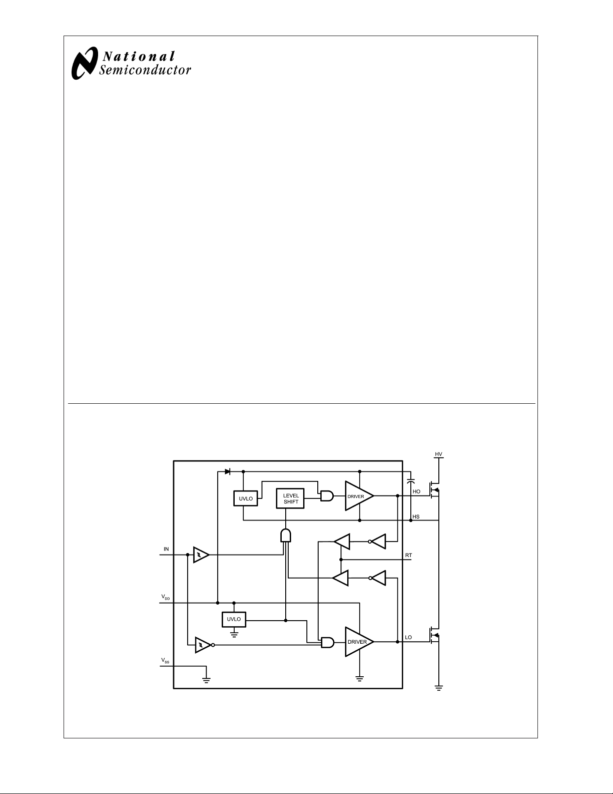
Simplified Block Diagram
20089003
FIGURE 1.
© 2004 National Semiconductor Corporation DS200890 www.national.com
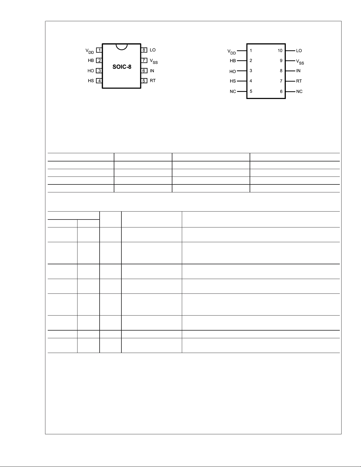
Connection Diagram
LM5104
8-Lead SOIC
See NS Package Number M08A
20089001
20089002
10-Lead LLP
See NS Package Number SDC10A
FIGURE 2.
Ordering Information
Ordering Number Package Type NSC Package Drawing Supplied As
LM5104M SOIC-8 M08A Shipped with Anti-Static Rails
LM5104MX SOIC-8 M08A 2500 shipped as Tape & Reel
LM5104SD LLP-10 SDC10A 1000 shipped as Tape & Reel
LM5104SDX LLP-10 SDC10A 4500 shipped as Tape & Reel
Pin Descriptions
Pin
SOIC-8 LLP-10
11V
2 2 HB High side gate driver
3 3 HO High side gate driver
4 4 HS High side MOSFET
5 7 RT Deadtime programming
6 8 IN Control input Logic 1 equals High Side ON and Low Side OFF. Logic 0 equals
79V
8 10 LO Low side gate driver
Note: For LLP-10 package, it is recommended that the exposed pad on the bottom of the LM5100 / LM5101 be soldered to ground plane on the PC board,
and the ground plane should extend out from beneath the IC to help dissipate the heat. Pins 5 and 6 have no connection.
Name Description Application Information
Positive gate drive supply Locally decouple to VSSusing low ESR/ESL capacitor, located as
DD
close to IC as possible.
Connect the positive terminal of bootstrap capacitor to the HB pin
bootstrap rail
and connect negative terminal to HS. The Bootstrap capacitor should
be placed as close to IC as possible.
Connect to gate of high side MOSFET with short low inductance
output
path.
Connect to bootstrap capacitor negative terminal and source of high
source connection
side MOSFET.
Resistor from RT to ground programs the deadtime between high
pin
and low side transitions.The resistor should be located close to the
IC to minimize noise coupling from adjacent traces.
High Side OFF and Low Side ON.
Ground return All signals are referenced to this ground.
SS
Connect to the gate of the low side MOSFET with a short low
output
inductance path.
www.national.com 2
LM5104
Absolute Maximum Ratings (Note 1)
If Military/Aerospace specified devices are required,
please contact the National Semiconductor Sales Office/
Storage Temperature Range –55˚C to +150˚C
ESD Rating HBM
2kV
(Note 2)
Distributors for availability and specifications.
to V
V
DD
SS
V
to V
HB
HS
IN to V
SS
LO Output –0.3V to V
HO Output V
V
to V
HS
SS
V
to V
HB
SS
RT to V
SS
HS
–0.3V to +18V
–0.3V to +18V
–0.3V to VDD+ 0.3V
+ 0.3V
DD
– 0.3V to VHB+ 0.3V
−1V to +100V
118V
–0.3V to 5V
Recommended Operating Conditions
V
DD
HS –1V to 100V
HB V
HS
HS Slew Rate
Junction Temperature –40˚C to +125˚C
+9V to +14V
+8VtoVHS+ 14V
<
50V/ns
Junction Temperature +150˚C
Electrical Characteristics Specifications in standard typeface are for T
type apply over the full operating junction temperature range. Unless otherwise specified, V
= +25˚C, and those in boldface
J
DD=VHB
= 12V, VSS=VHS=
0V, RT = 100kΩ. No Load on LO or HO.
Symbol Parameter Conditions Min Typ Max Units
SUPPLY CURRENTS
I
DD
I
DDO
I
HB
I
HBO
I
HBS
I
HBSO
VDDQuiescent Current LI = HI = 0V 0.4 0.6 mA
VDDOperating Current f = 500 kHz 1.9 3 mA
Total HB Quiescent Current LI = HI = 0V 0.06 0.2 mA
Total HB Operating Current f = 500 kHz 1.3 3 mA
HB to VSSCurrent, Quiescent VHS=VHB= 100V 0.05 10 µA
HB to VSSCurrent, Operating f = 500 kHz 0.08 mA
INPUT PINS
V
IL
V
IH
R
I
Low Level Input Voltage Threshold 0.8 1.8 V
High Level Input Voltage Threshold 1.8 2.2 V
Input Pulldown Resistance 100 200 500 kΩ
TIME DELAY CONTROLS
V
RT
I
RT
T
D1
T
D2
Nominal Voltage at RT 2.7 3 3.3 V
RT Pin Current Limit RT = 0V 0.75 1.5 2.25 mA
Delay Timer, RT = 10 kΩ 58 90 130 ns
Delay Timer, RT = 100 kΩ 140 200 270 ns
UNDER VOLTAGE PROTECTION
V
DDR
V
DDH
V
HBR
V
HBH
VDDRising Threshold 6.0 6.9 7.4 V
VDDThreshold Hysteresis 0.5 V
HB Rising Threshold 5.7 6.6 7.1 V
HB Threshold Hysteresis 0.4 V
BOOT STRAP DIODE
V
DL
V
DH
R
D
Low-Current Forward Voltage I
High-Current Forward Voltage I
Dynamic Resistance I
= 100 µA 0.60 0.9 V
VDD-HB
= 100 mA 0.85 1.1 V
VDD-HB
= 100 mA 0.8 1.5 Ω
VDD-HB
LO GATE DRIVER
V
V
I
I
OLL
OHL
OHL
OLL
Low-Level Output Voltage ILO= 100 mA 0.25 0.4 V
High-Level Output Voltage ILO= – 100 mA
V
OHL=VDD–VLO
0.35 0.55 V
Peak Pullup Current VLO= 0V 1.6 A
Peak Pulldown Current VLO= 12V 1.8 A
HO GATE DRIVER
V
OLH
Low-Level Output Voltage IHO= 100 mA 0.25 0.4 V
www.national.com3
Electrical Characteristics Specifications in standard typeface are for T
apply over the full operating junction temperature range. Unless otherwise specified, V
LM5104
RT = 100kΩ. No Load on LO or HO. (Continued)
= +25˚C, and those in boldface type
J
DD=VHB
= 12V, VSS=VHS= 0V,
Symbol Parameter Conditions Min Typ Max Units
V
I
I
OHH
OHH
OLH
High-Level Output Voltage IHO= – 100 mA,
V
OHH=VHB–VHO
0.35 0.55 V
Peak Pullup Current VHO= 0V 1.6 A
Peak Pulldown Current VHO= 12V 1.8 A
THERMAL RESISTANCE
θ
JA
Junction to Ambient SOIC-8 170 ˚C/W
LLP-10 (Note 3) 40
Switching Characteristics Specifications in standard typeface are for T
type apply over the full operating junction temperature range. Unless otherwise specified, V
= +25˚C, and those in boldface
J
DD=VHB
= 12V, VSS=VHS=
0V, No Load on LO or HO .
Symbol Parameter Conditions Min Typ Max Units
t
LPHL
t
HPHL
t
RC,tFC
t
R,tF
Lower Turn-Off Propagation Delay (IN
Rising to LO Falling)
Upper Turn-Off Propagation Delay (IN
Falling to HO Falling)
25 56 ns
25 56 ns
Either Output Rise/Fall Time CL= 1000 pF 15 ns
Either Output Rise/Fall Time
CL= 0.1 µF 0.6 µs
(3V to 9V)
t
BS
Note 1: Absolute Maximum Ratings indicate limits beyond which damage to the component may occur. Operating Ratings are conditions under which operation of
the device is guaranteed. Operating Ratings do not imply guaranteed performance limits. For guaranteed performance limits and associated test conditions, see the
Electrical Characteristics tables.
Note 2: The human body model is a 100 pF capacitor discharged through a 1.5kΩ resistor into each pin. 2 kV for all pins except Pin 2, Pin 3 and Pin 4 which are
rated at 500V.
Note 3: 4 layer board with Cu finished thickness 1.5/1/1/1.5 oz. Maximum die size used. 5x body length of Cu trace on PCB top. 50 x 50mm ground and power
planes embedded in PCB. See Application Note AN-1187.
Note 4: Min and Max limits are 100% production tested at 25˚C. Limits over the operating temperature range are guaranteed through correlation using Statistical
Quality Control (SQC) methods. Limits are used to calculate National’s Average Outgoing Quality Level (AOQL).
Note 5: The θ
Bootstrap Diode Turn-Off Time IF= 20 mA, IR= 200 mA 50 ns
is not a given constant for the package and depends on the printed circuit board design and the operating environment.
JA
www.national.com 4
 Loading...