

December 2004
LM5070
Integrated Power Over Ethernet PD Interface and PWM
Controller
General Description
The LM5070 power interface port and pulse width modulation (PWM) controller provides a complete integrated solution for Powered Devices (PD) that connect into Power over
Ethernet (PoE) systems. The LM5070 integrates an 80V,
400mA line connection switch and associated control for a
fully IEEE 802.3af compliant interface with a full featured
current mode pulse width modulator dc-dc converter. All
power sequencing requirements between the controller interface and switch mode power supply (SMPS) are integrated into the IC. Two options are available providing either
an 80% maximum duty cycle limit with slope compensation
(on the –80 suffix) device or a 50% maximum duty cycle limit
and no slope compensation on the (– 50 suffix) device.
Features
n Fully Compliant 802.3af Power Interface Port
n 80V, 1Ω, 400 mA Internal MOSFET
n Programmable Inrush Current Limit
n Detection Resistor Disconnect Function
n Programmable Classification Current
n Programmable Under-voltage Lockout with
Programmable Hysteresis
n Thermal Shutdown Protection
n Current Mode Pulse Width Modulator
n Supports both Isolated and Non-Isolated Applications
n Error Amplifier and Reference for Non-Isolated
Applications
n Programmable Oscillator Frequency
n Programmable Soft-start
n 80% Maximum Duty Cycle Limiter, Slope Compensation
(-80 device)
n 50% Maximum Duty Cycle Limiter, No Slope
Compensation (-50 device)
n 800 mA Peak Gate Driver
Packages
n TSSOP-16
n LLP-16 (5 mmx5mm)
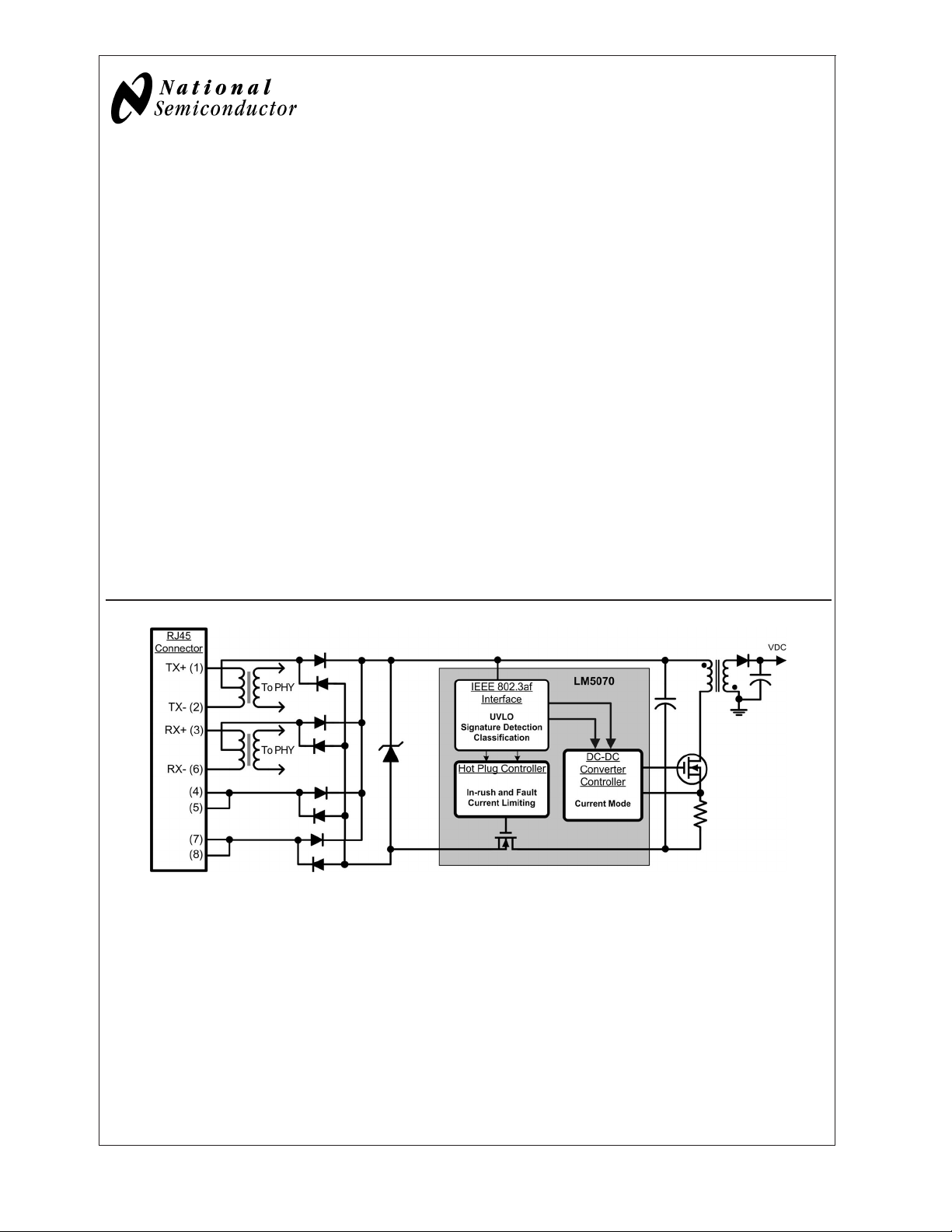
LM5070 Integrated Power Over Ethernet PD Interface and PWM Controller
20120001
© 2004 National Semiconductor Corporation DS201200 www.national.com
LM5070
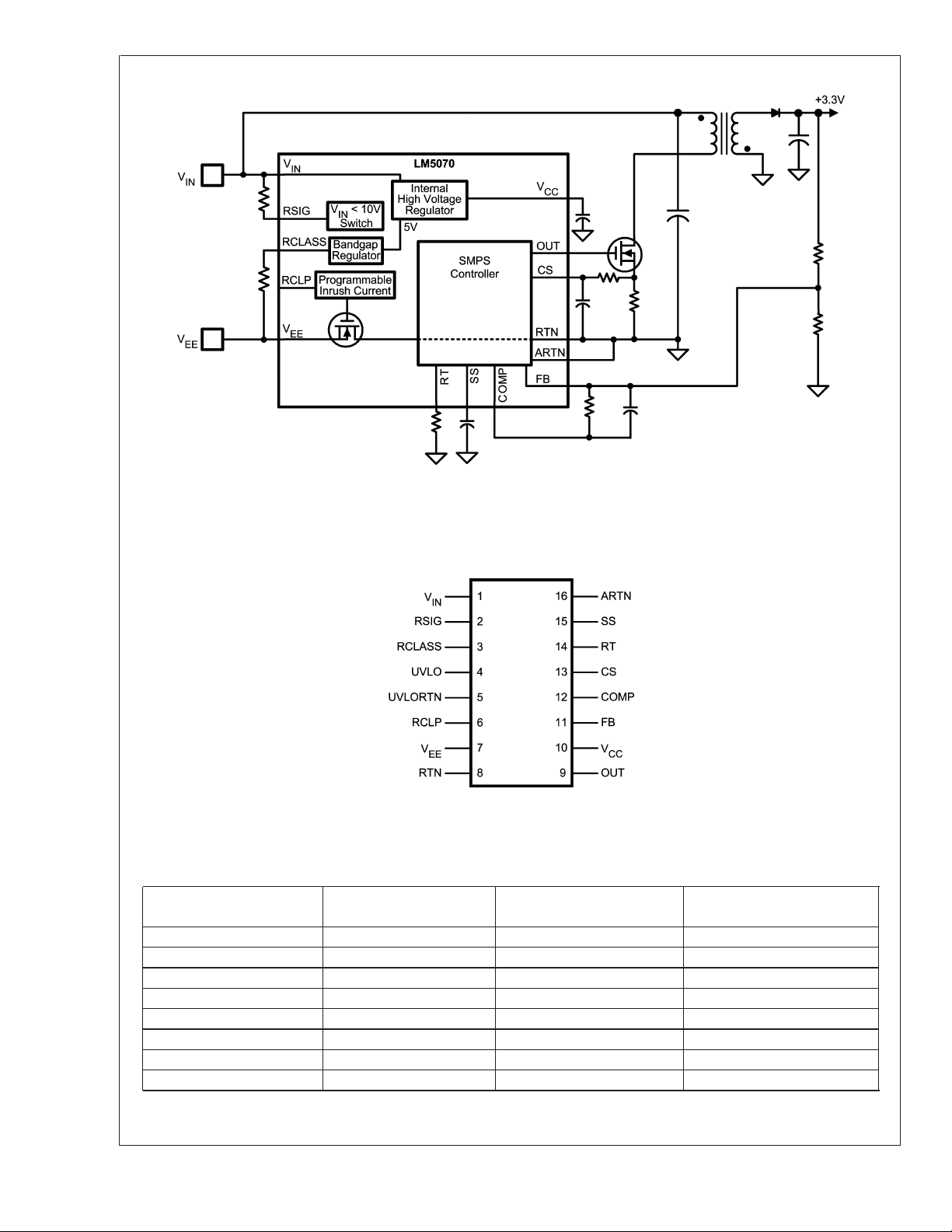
Connection Diagram
20120002
FIGURE 1. Simplified Block Diagram
16 Lead TSSOP, LLP
20120003
Ordering Information
NSC Package Type /
Order Number Description
LM5070MTC-50 50% Duty Cycle Limit TSSOP-16/MTC-16 92 units per rail
LM5070MTCX-50 50% Duty Cycle Limit TSSOP-16/MTC-16 2500 units on tape and reel
LM5070SD-50 50% Duty Cycle Limit LLP-16/SDA-16 Available Soon
LM5070SDX-50 50% Duty Cycle Limit LLP-16/SDA-16 Available Soon
LM5070MTC-80 80% Duty Cycle Limit TSSOP-16/MTC-16 92 units per rail
LM5070MTCX-80 80% Duty Cycle Limit TSSOP-16/MTC-16 2500 units on tape and reel
LM5070SD-80 80% Duty Cycle Limit LLP-16/SDA-16 Available Soon
LM5070SDX-80 80% Duty Cycle Limit LLP-16/SDA-16 Available Soon
www.national.com 2
Drawing Supplied As
Pin Description
PIN NAME DESCRIPTION APPLICATION INFORMATION
1V
2 RSIG Signature resistor pin. Connect a 25kΩ signature resistor from V
3 RCLASS Classification resistor pin. Connect the classification programming resistor from this pin to
4 UVLO Line under-voltage lockout. An external resistor divider from V
5 UVLORTN Return for the external UVLO resistors, if
6 RCLP Current limit programming pin. Programs the inrush current limit for the device. If left open, the
7V
8 RTN System return for the PWM converter. The drain of the internal current limiting power MOSFET which
9 OUT Output of the PWM controller. DC-DC converter gate driver output with 800mA peak sink current
10 V
11 FB Feedback signal. Inverting input of the internal error amplifier. The non-inverting
12 COMP The output of the error amplifier and
13 CS Current sense input. Current sense input for current mode control and over-current
14 RT / SYNC Oscillator timing resistor pin and
15 SS Soft-start input. An external capacitor and an internal 10uA current source set the
16 ARTN Analog PWM supply return. RTN for sensitive analog circuitry including the SMPS current limit
— EP Exposed PAD, underside of the LLP
System high potential input. The diode “OR” of several lines entering the PD, it is the more
IN
positive input potential.
to this pin for signature
IN
detection.
.
V
EE
to UVLORTN programs the
IN
shutdown levels with a 2.00V threshold at the UVLO pin.
Hysteresis is set by a switched internal 10uA current source that
forces additional current into the resistor divider.
Connect the bottom resistor of the resistor divider between the
used.
UVLO pin and this pin.
inrush current limit will default to 400mA max.
System low potential input. Diode “OR’d” to the RJ45 connector and PSE’s –48V supply, it is
EE
the more negative input potential.
connects V
to the return path of the dc-dc converter.
EE
capability.
Output of the internal high voltage series
CC
pass regulator. Regulated output voltage
is nominally 7.8V.
When the auxiliary transformer winding (if used) raises the voltage
on this pin above the regulation set point, the internal series pass
regulator will shutdown, reducing the controller power dissipation.
input is internally connected to a 1.25V reference.
COMP pull-up is provided by an internal 5K resistor which may be
input to the Pulse Width Modulator.
used to bias an opto-coupler transistor.
protection. Current limiting is accomplished using a dedicated
current sense comparator. If the CS pin voltage exceeds 0.5V the
OUT pin switches low for cycle-by-cycle current limiting. CS is held
low for 50ns after OUT switches high to blank leading edge current
spikes.
An external resistor connected from RT to ARTN sets the oscillator
synchronization input.
frequency. This pin will also accept narrow ac-coupled
synchronization pulses from an external clock.
soft-start ramp rate.
amplifier.
Internally bonded to the die substrate. Connect to V
package option.
low thermal impedance.
potential for
EE
LM5070
www.national.com3
Absolute Maximum Ratings (Note 1)
If Military/Aerospace specified devices are required,
LM5070
please contact the National Semiconductor Sales Office/
Distributors for availability and specifications.
,RTN to V
V
IN
RSIG to V
UVLO to V
EE
IN
EE
-0.3V to 80V
-12V to 0V
-0.3V to 57V
Human Body Model 2000V
Storage Temperature -65˚C to +150˚C
Junction Temperature 150˚C
Lead Temperature (Note 2)
Wave (4 seconds)
Infrared (10 seconds)
Vapor Phase (75 seconds)
UVLORTN -0.3V to 13V
RCLASS, RCLP to V
EE
ARTN to RTN -0.3V to 0.3V
V
, OUT to ARTN -0.3V to 16V
CC
All other inputs to ARTN -0.3V to 7V
ESD Rating
-0.3V to 7V
Operating Ratings
VINvoltage 1.8V to 75V
External voltage applied to V
CC
Operating Junction Temperature -40˚C to +125˚C
8.1V to 15V
Electrical Characteristics (Note 3)
Specifications in standard type face are for TJ= +25˚C and those in boldface type apply over the full operating junction temperature range. Unless otherwise specified: V
Symbol Parameter Conditions Min Typ Max Units
Powered Interface
IOS Offset Current V
VCLSS(ON) Signature Resistor Disable /
Classification Current Turn On
VCLSS(OFF) Classification Current Turn Off VINwith respect to V
Classification Voltage With respect to V
ICLASS Supply Current During
Classification
IDC Supply Current During Normal
Operation
UVLO Pin Reference Voltage V
UVLO Hysteresis Current V
Softstart Release RTN falling with respect
Softstart Release Hysteresis RTN rising with respect
RDS(ON) PowerFET Resistance I = 350mA,
ILEAK SMPS Bias Current V
ILIM Default Current Limit V
ILIM Default Current Limit V
Current Limit Programming
Accuracy
Startup Regulator
VccReg V
Regulation Open ckt 7.5 7.8 8.1 V
CC
V
Current Limit (Note 4) 15 20 mA
CC
= 48V, VCC= 10V, RT = 30.3kΩ.
IN
<
10.0V 10 V
IN
V
with respect to V
IN
V
=17V 0.5 1.5 mA
IN
EE
EE
EE
10.0 11.5 12.5 V
20.5 22.0 23.0 V
1.43 1.5 1.57 V
OUT floating 1 1.9 mA
>
12V 1.95 2.00 2.05 V
IN
>
UVLO 8.0 10 11.5 uA
IN
1.2 1.45 1.7 V
to V
EE
0.8 1.1 1.3 V
to V
EE
1 2.2 Ω
= 48V
V
IN
= 0V, VIN= RTN =
EE
100 uA
57V
= 0V, RTN = 3.0V,
EE
350 390 420 mA
Temp = 0˚C to 85˚C
= 0V, RTN = 3.0V,
EE
325 390 420 mA
Temp = -40˚C to 125˚C
VEE= 0V, RTN = 3.0V,
-20 +20 %
RCLP = 80.6kΩ
260˚C
240˚C
219˚C
www.national.com 4
Electrical Characteristics (Note 3) (Continued)
Specifications in standard type face are for TJ= +25˚C and those in boldface type apply over the full operating junction temperature range. Unless otherwise specified: V
Symbol Parameter Conditions Min Typ Max Units
V
Supply
CC
V
UVLO (Rising) VccReg –
CC
UVLO (Falling) 5.9 6.25 6.6 V
V
CC
Supply Current (Icc) Cload = 0 1.5 3 mA
Error Amplifier
GBW Gain Bandwidth 4 MHz
DC Gain 75 dB
Input Voltage FB = COMP 1.219
COMP Sink Capability FB=1.5V COMP=1V 5 20 mA
Current Limit
ILIM Delay to Output CS step from 0 to 0.6V,
Cycle by Cycle Current Limit
Threshold Voltage
Leading Edge Blanking Time 55 ns
CS Sink Impedance (clocked) 25 55 Ω
Softstart
Softstart Current Source 7 10 13 uA
Oscillator(Note 5)
Frequency1
(RT = 30.3K)
Frequency2
(RT = 10.5K)
Sync threshold 3.1 3.8 V
PWM Comparator
Delay to Output COMP set to 2V
Min Duty Cycle COMP=0V 0 %
Max Duty Cycle (-80 Device) 80 %
Max Duty Cycle (-50 Device) 50 %
COMP to PWM Comparator
Gain
COMP Open Circuit Voltage 4.5 5.4 6.3 V
COMP Short Circuit Current COMP= 0V 0.6 1.1 1.5 mA
Slope Compensation
Slope Comp Amplitude
(LM5070-80 Device Only)
Output Section
Output High Saturation I
Output Low Saturation I
Rise time Cload = 1nF 15 ns
Fall time Cload = 1nF 15 ns
= 48V, VCC= 10V, RT = 30.3kΩ.
IN
VccReg –
300mV
100mV
1.281
1.212
1.288
20 ns
time to onset of OUT
transition (90%)
0.44 0.5 0.56 V
175 200 225 KHz
505 580 665 KHz
25 ns
CS stepped 0 to 0.4V,
time to onset of OUT
transition low
0.33
Delta increase at PWM
105 mV
Comparator to CS
= 50mA,
out
V
CC-VOUT
= 100mA 0.25 0.75 V
out
0.25 0.75 V
V
LM5070
www.national.com5
Electrical Characteristics (Note 3) (Continued)
Specifications in standard type face are for TJ= +25˚C and those in boldface type apply over the full operating junction tem-
LM5070
perature range. Unless otherwise specified: V
Symbol Parameter Conditions Min Typ Max Units
Thermal Shutdown
Tsd Thermal Shutdown Temp. 165 ˚C
Thermal
Shutdown
Hysteresis
Thermal Resistance
θ
JA
Note 1: Absolute Maximum Ratings are limits beyond which damage to the device may occur. Operating Ratings are conditions under which operation of the device
is intended to be functional. For guaranteed specifications and test conditions, see the Electrical Characteristics.
Note 2: For detailed information on soldering plastic TSSOP and LLP package, refer to the Packaging Databook available from National Semiconductor.
Note 3: Min and Max limits are 100% production tested at 25 ˚C. Limits over the operating temperature range are guaranteed through correlation using Statistical
Quality Control (SQC) methods. Limits are used to calculate National’s Average Outgoing Quality Level (AOQL).
Note 4: Device thermal limitations may limit usable range.
Note 5: Specification applies to the oscillator frequency. The operational frequency of the LM5070-50 devices is divided by two.
Junction to Ambient MTC Package 125 ˚C/W
= 48V, VCC= 10V, RT = 30.3kΩ.
IN
25 ˚C
SDA Package 32 ˚C/W
www.national.com 6
 Loading...