

National Semiconductor LM5035A Technical data
July 30, 2008
LM5035A
PWM Controller with Integrated Half-Bridge and SyncFET
Drivers
LM5035A PWM Controller with Integrated Half-Bridge and SyncFET Drivers
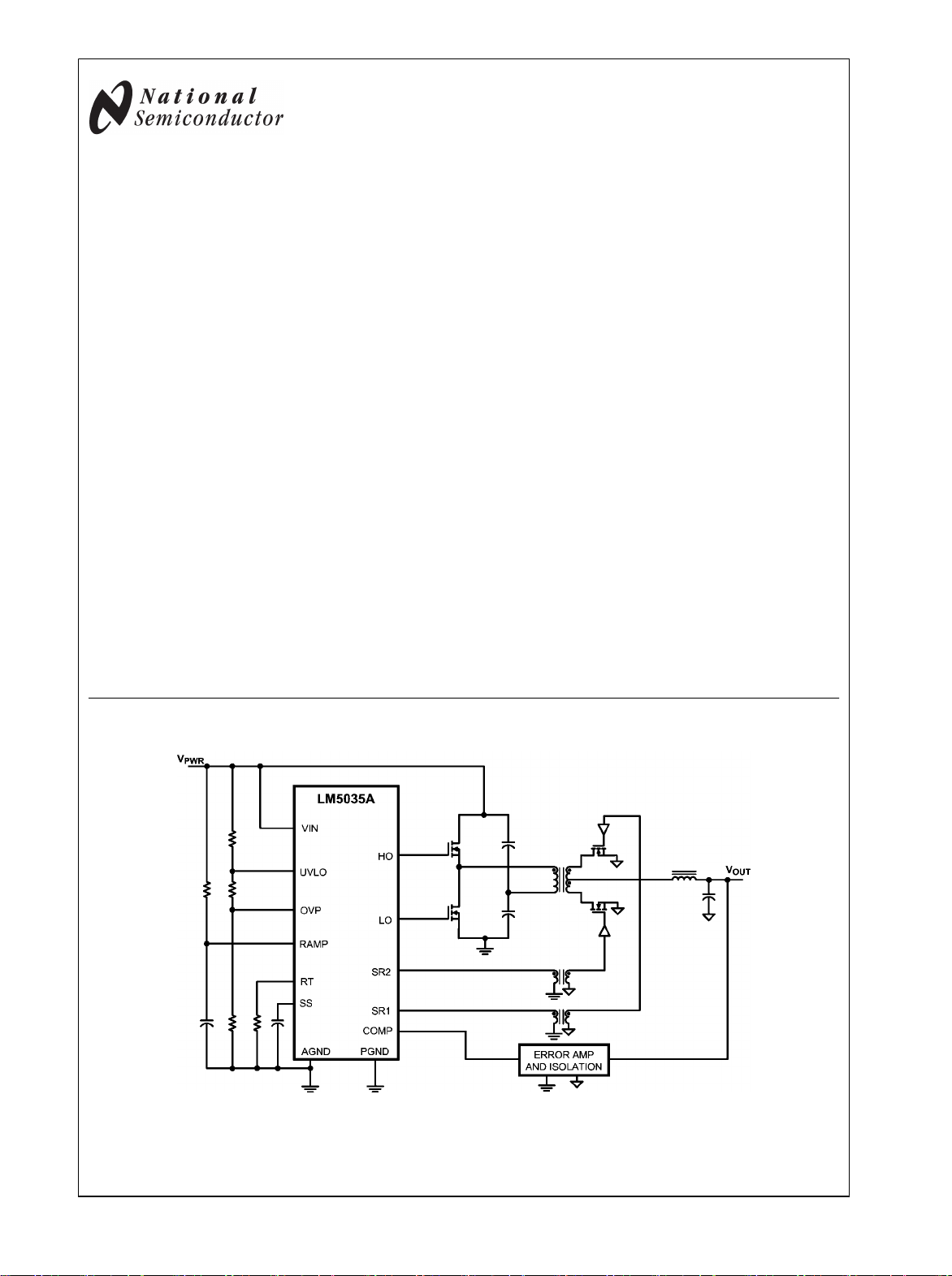
General Description
The LM5035A Half-Bridge Controller/Gate Driver contains all
of the features necessary to implement half-bridge topology
power converters using voltage mode control with line voltage
feed-forward. The LM5035A is a functional variant of the
LM5035 half-bridge PWM controller. The VCC current limit
threshold has been increased to 35 mA. The soft start and
soft start currents have been increased from 50 µA to 100 µA.
The BST UV threshold has been lowered to less than the VCC
UV threshold. The ratio of the T1 and T2 delays on the SR1
and SR2 outputs has been increased from 2:1 to 3:1. The
floating high-side gate driver is capable of operating with supply voltages up to 105V. Both the high-side and low-side gate
drivers are capable of 2A peak. An internal high voltage startup regulator is included, along with programmable line undervoltage lockout (UVLO) and overvoltage protection (OVP).
The oscillator is programmed with a single resistor to frequencies up to 2MHz. The oscillator can also be synchronized
to an external clock. A current sense input and a programmable timer provide cycle-by-cycle current limit and adjustable hiccup mode overload protection.
Simplified Application Diagram
Features
105V / 2A Half-Bridge Gate Drivers
■
Synchronous Rectifier Control Outputs with
■
Programmable Delays
High Voltage (105V) Start-up Regulator
■
Voltage mode Control with Line Feed-Forward and Volt •
■
Second Limiting
Resistor Programmed, 2MHz Capable Oscillator
■
Patent Pending Oscillator Synchronization
■
Programmable Line Under-Voltage Lockout
■
Line Over-Voltage Protection
■
Internal Thermal Shutdown Protection
■
Adjustable Soft-Start
■
Versatile Dual Mode Over-Current Protection with Hiccup
■
Delay Timer
Cycle-by-Cycle Over-Current Protection
■
Direct Opto-coupler Interface
■
5V Reference Output
■
Packages
TSSOP-20EP (Thermally enhanced)
■
LLP-24 (4mm x 5mm)
■
30034101
© 2008 National Semiconductor Corporation 300341 www.national.com
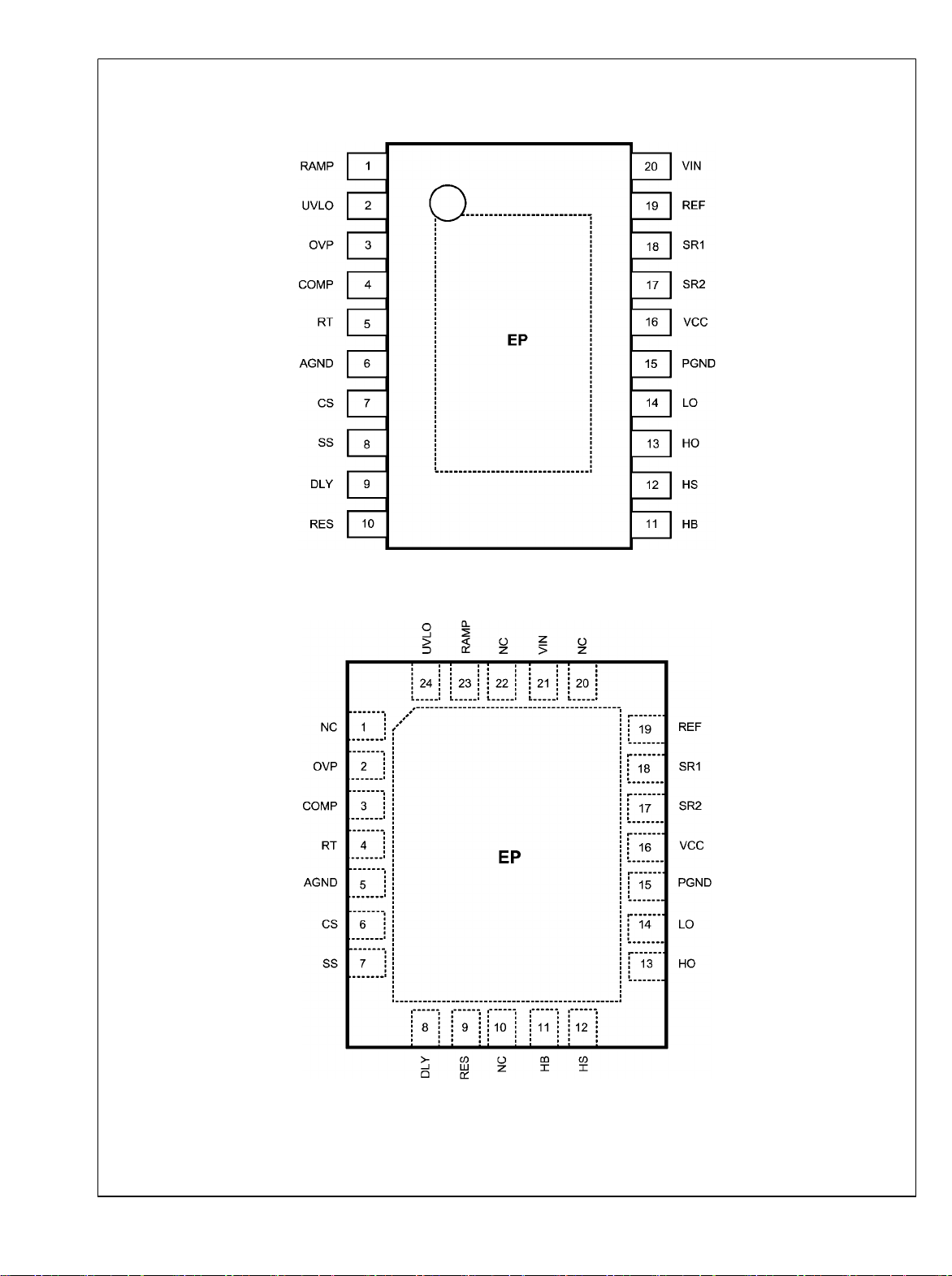
Connection Diagrams
LM5035A
Top View
20-Lead TSSOP EP
30034102
Top View
LLP-24 Package
www.national.com 2
30034103
Ordering Information
Order Number Package Type NSC Package Drawing Supplied As
LM5035AMH TSSOP-20EP MXA20A 73 Units per Rail
LM5035AMHX TSSOP-20EP MXA20A 2500 Units on Tape and Reel
LM5035ASQ LLP-24 SQA24B 1000 Units on Tape and Reel
LM5035ASQX LLP-24 SQA24B 4500 Units on Tape and Reel
Pin Descriptions
LM5035A
TSSOP
PIN
LLP PIN Name Description Application Information
1 23 RAMP Modulator ramp signal An external RC circuit from VIN sets the ramp slope. This pin is
discharged at the conclusion of every cycle by an internal FET.
Discharge is initiated by either the internal clock or the Volt •
Second clamp comparator.
2 24 UVLO Line Under-Voltage Lockout An external voltage divider from the power source sets the
shutdown and standby comparator levels. When UVLO reaches
the 0.4V threshold the VCC and REF regulators are enabled.
When UVLO reaches the 1.25V threshold, the SS pin is released
and the device enters the active mode. Hysteresis is set by an
internal current sink that pulls 23 µA from the external resistor
divider.
3 2 OVP Line Over-Voltage Protection An external voltage divider from the power source sets the
shutdown levels. The threshold is 1.25V. Hysteresis is set by an
internal current source that sources 23µA into the external
resistor divider.
4 3 COMP Input to the Pulse Width Modulator An external opto-coupler connected to the COMP pin sources
current into an internal NPN current mirror. The PWM duty cycle
is maximum with zero input current, while 1mA reduces the duty
cycle to zero. The current mirror improves the frequency
response by reducing the AC voltage across the opto-coupler
detector.
5 4 RT Oscillator Frequency Control and
Sync Clock Input.
6 5 AGND Analog Ground Connect directly to Power Ground.
7 6 CS Current Sense input for current
limit
8 7 SS Soft-start Input An internal 110 µA current source charges an external capacitor
9 8 DLY Timing programming pin for the
LO and HO to SR1 and SR2
outputs.
10 9 RES Restart Timer If cycle-by-cycle current limit is exceeded during any cycle, a 22
Normally biased at 2V. An external resistor connected between
RT and AGND sets the internal oscillator frequency. The internal
oscillator can be synchronized to an external clock with a
frequency higher than the free running frequency set by the RT
resistor.
If CS exceeds 0.25V the output pulse will be terminated, entering
cycle-by-cycle current limit. An internal switch holds CS low for
50ns after HO or LO switches high to blank leading edge
transients.
to set the soft-start rate. During a current limit restart sequence,
the internal current source is reduced to 1.2µA to increase the
delay before retry.
An external resistor to ground sets the timing for the non-overlap
time of HO to SR1 and LO to SR2.
µA current is sourced to the RES pin capacitor. If the RES
capacitor voltage reaches 2.5V, the soft-start capacitor will be
fully discharged and then released with a pull-up current of 1.2µA.
After the first output pulse at LO (when SS > COMP offset,
typically 1V), the SS pin charging current will revert to 110 µA.
3 www.national.com
TSSOP
PIN
LM5035A
LLP PIN Name Description Application Information
11 11 HB Boost voltage for the HO driver An external diode is required from VCC to HB and an external
capacitor is required from HS to HB to power the HO gate driver.
12 12 HS Switch node Connection common to the transformer and both power switches.
Provides a return path for the HO gate driver.
13 13 HO High side gate drive output. Output of the high side PWM gate driver. Capable of sinking 2A
peak current.
14 14 LO Low side gate drive output. Output of the low side PWM gate driver. Capable of sinking 2A
peak current.
15 15 PGND Power Ground Connect directly to Analog Ground.
16 16 VCC Output of the high voltage start-up
regulator. The VCC voltage is
regulated to 7.6V.
17 17 SR2 Synchronous rectifier driver
output.
18 18 SR1 Synchronous rectifier driver
output.
19 19 REF Output of 5V Reference Maximum output current is 20mA. Locally decoupled with a 0.1µF
20 21 VIN Input voltage source Input to the Start-up Regulator. Operating input range is 13V to
EP EP EP Exposed Pad, underside of
package
1 NC No connection No electrical contact.
10 NC No connection No electrical contact.
20 NC No connection No electrical contact.
22 NC No connection No electrical contact.
If an auxiliary winding raises the voltage on this pin above the
regulation setpoint, the Start-up Regulator will shutdown, thus
reducing the internal power dissipation.
Control output of the synchronous FET gate. Capable of 0.5A
peak current.
Control output of the synchronous FET gate. Capable of 0.5A
peak current.
capacitor.
100V with transient capability to 105V. For power sources outside
of this range, the LM5035A can be biased directly at VCC by an
external regulator.
No electrical contact. Connect to system ground plane for
reduced thermal resistance.
www.national.com 4
LM5035A
Absolute Maximum Ratings (Note 1)
If Military/Aerospace specified devices are required,
please contact the National Semiconductor Sales Office/
Distributors for availability and specifications.
VIN to GND -0.3V to 105V
HS to GND -1V to 105V
HB to GND -0.3V to 118V
HB to HS -0.3V to 18V
VCC to GND -0.3V to 16V
All other inputs to GND -0.3V to 7V
ESD Rating (Note 4)
Human Body Model 2kV
Storage Temperature Range -65°C to 150°C
Junction Temperature 150°C
Operating Ratings (Note 1)
VIN Voltage 13V to 105V
External Voltage Applied to VCC 8V to 15V
Operating Junction Temperature -40°C to +125°C
CS, RT, DLY to GND -0.3V to 5.5V
COMP Input Current 10mA
Electrical Characteristics Specifications with standard typeface are for T
apply over full Operating Junction Temperature range. V
27.4kΩ, V
UVLO
= 3V, V
= 0V unless otherwise stated. See (Note 2) and (Note 3).
OVP
= 48V, V
VIN
= 10V externally applied, RRT = 15.0 kΩ, R
VCC
= 25°C, and those with boldface type
J
DLY
Symbol Parameter Conditions Min Typ Max Units
Startup Regulator (VCC pin)
V
VCC
I
VCC(LIM)
V
VCCUV
VCC voltage I
VCC current limit V
VCC Under-voltage threshold (VCC
increasing)
= 10mA 7.3 7.6 7.9 V
VCC
= 7V 25 35 mA
VCC
VIN = VCC, ΔV
from the regulation
VCC
0.2 0.1 V
setpoint
VCC decreasing VCC – PGND 5.5 6.2 6.9 V
I
VIN
Supply current into VCC from
Startup regulator current VIN = 90V, UVLO = 0V 30 70 µA
external source
Outputs & COMP open, V
Outputs Switching
VCC
= 10V,
4 6 mA
Voltage Reference Regulator (REF pin)
V
REF
REF Voltage Regulation I
REF Voltage I
= 0mA 4.85 5 5.15 V
REF
= 0 to 10mA 25 50 mV
REF
REF Current Limit REF = 4.5V 15 20 mA
Under-Voltage Lock Out and shutdown (UVLO pin)
V
I
UVLO
UVLO
Under-voltage threshold 1.212 1.25 1.288 V
Hysteresis current UVLO pin sinking 19 23 27 µA
Under-voltage Shutdown Threshold UVLO voltage falling 0.3 V
Under-voltage Standby Enable
UVLO voltage rising 0.4 V
Threshold
Over-Voltage Protection (OVP pin)
V
I
OVP
OVP
Over-Voltage threshold 1.212 1.25 1.288 V
Hysteresis current OVP pin sourcing 19 23 27 µA
Current Sense Input (CS Pin)
V
CS
CS delay to output CS from zero to 1V. Time for HO and LO
Current Limit Threshold 0.228 0.25 0.272 V
80 ns
to fall to 90% of VCC. Output load = 0 pF.
Leading edge blanking time at CS 50 ns
CS sink impedance (clocked) Internal FET sink impedance 32 60
Current Limit Restart (RES Pin)
V
RES
Charge source current V
Discharge sink current V
RES Threshold 2.4 2.5 2.6 V
= 1.5V 16 22 28 µA
RES
= 1V 8 12 16 µA
RES
=
Ω
5 www.national.com
Symbol Parameter Conditions Min Typ Max Units
Soft-Start (SS Pin)
LM5035A
I
SS
Charging current in normal
VSS = 0 80 110 140 µA
operation
Charging current during a hiccup
VSS = 0 0.6 1.2 1.8 µA
mode restart
Soft-stop Current Sink VSS = 2.5V 80 110 140 µA
Oscillator (RT Pin)
F
F
SW1
SW2
Frequency 1 (at HO, half oscillator
frequency)
Frequency 2 (at HO, half oscillator
RRT = 15 kΩ, TJ = 25°C
RRT = 15 kΩ, TJ = -40°C to 125°C
RRT = 5.49 kΩ
185 200 215 kHz
180 220
430 500 570 kHz
frequency)
DC level 2 V
Input Sync threshold 2.5 3 3.4 V
PWM Controller (Comp Pin)
Delay to output 80 ns
V
PWM-OS
SS to RAMP offset 0.7 1 1.2 V
Minimum duty cycle SS = 0V 0 %
Small signal impedance I
= 600µA, COMP current to PWM
COMP
5000
voltage
Main Output Drivers (HO and LO Pins)
Output high voltage I
Output low voltage I
Rise time C
Fall time C
Deadtime, HO to LO, LO to HO V
Peak source current V
Peak sink current V
= 50mA, VHB - VHO, V
OUT
= 100 mA 0.2 0.5 V
OUT
= 1 nF 15 ns
LOAD
= 1 nF 13 ns
LOAD
= V
, I
DLY
HO,LO
HO,LO
REF
= 0V, V
= 10V, V
= 0mA 45 70 100 ns
COMP
= 10V 1.25 A
VCC
= 10V 2 A
VCC
VCC
- V
LO
0.5 0.25 V
HB Threshold VCC rising 3.8 V
Voltage Feed-Forward (RAMP Pin)
RAMP comparator threshold COMP current = 0 2.4 2.5 2.6 V
Synchronous Rectifier Drivers (SR1, SR2)
Output high voltage I
Output low voltage I
Rise time C
Fall time C
Peak source current VSR = 0, V
Peak sink current VSR = V
T1 Deadtime, SR1 falling to HO rising,
SR2 falling to LO rising
T2 Deadtime, HO falling to SR1 rising,
LO falling to SR2 rising
= 10mA, V
OUT
= 20 mA (sink) 0.08 0.2 V
OUT
= 1 nF 40 ns
LOAD
= 1 nF 20 ns
LOAD
VCC
VCC
R
= 10k 33 ns
DLY
R
= 27.4k 68 86 120 ns
DLY
R
= 100k 300 ns
DLY
R
= 10k 18 ns
DLY
R
= 27.4k 20 29 42 ns
DLY
R
= 100k 80 ns
DLY
- V
, V
VCC
SR1
VCC
- V
SR2
0.25 0.1 V
= 10V 0.5 A
, V
= 10V 0.5 A
VCC
Ω
www.national.com 6

Symbol Parameter Conditions Min Typ Max Units
Thermal Shutdown
T
SD
Shutdown temperature 165 °C
Hysteresis 20 °C
Thermal Resistance
θ
JA
Junction to ambient, 0 LFPM Air
TSSOP-20_EP package 40 °C/W
Flow
θ
JC
Junction to Case (EP) Thermal
TSSOP-20_EP package 4 °C/W
resistance
θ
JA
θ
JC
Note 1: Absolute Maximum Ratings are limits beyond which damage to the device may occur. Operating Ratings are conditions under which operation of the
device is intended to be functional. For guaranteed specifications and test conditions, see the Electrical Characteristics.
Note 2: All limits are guaranteed. All electrical characteristics having room temperature limits are tested during production with TA = 25°C. All hot and cold limits
are guaranteed by correlating the electrical characteristics to process and temperature variations and applying statistical process control.
Note 3: Typical specifications represent the most likely parametric norm at 25°C operation
Note 4: The human body model is a 100 pF capacitor discharged through a 1.5 kΩ resistor into each pin. 2kV for all pins except HB, HO and HS which are rated
at 1.5kV.
Junction to ambient, 0 LFM Air Flow LLP-24 (4 mm x 5 mm) 40 °C/W
Junction to Case Thermal resistance LLP-24 (4 mm x 5 mm) 6 °C/W
LM5035A
7 www.national.com
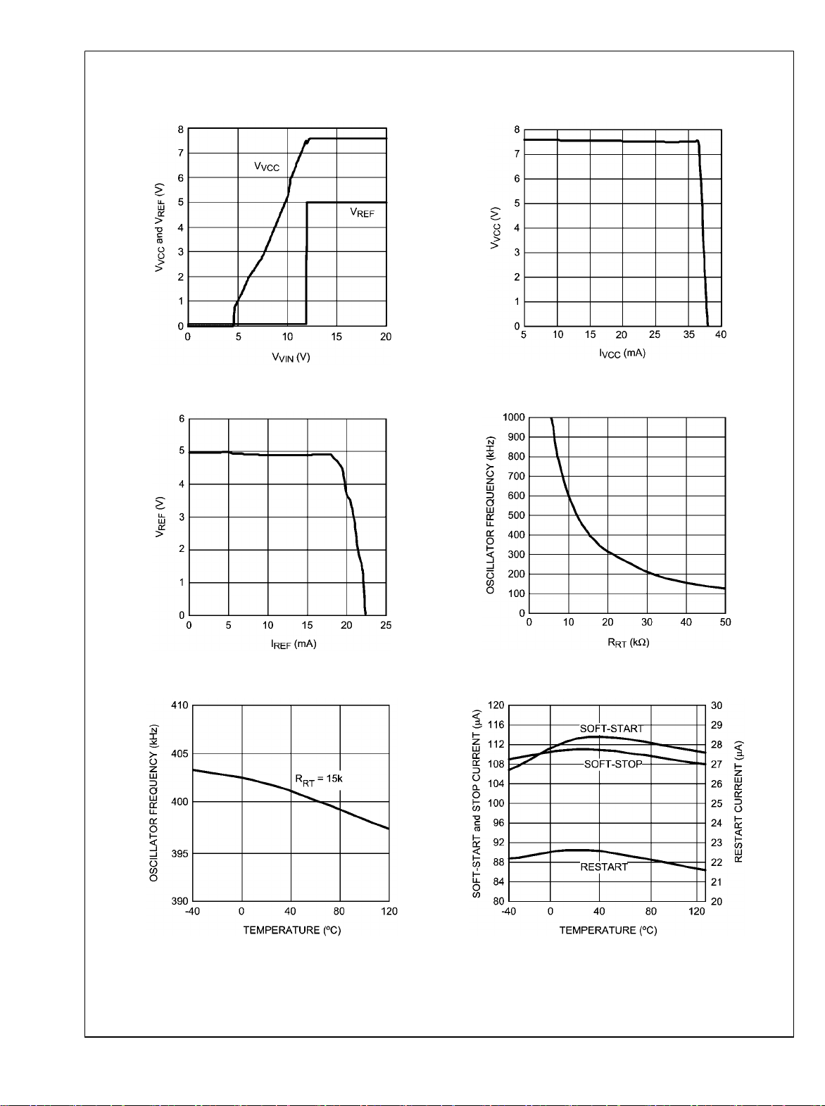
Typical Performance Characteristics
V
LM5035A
VCC
and V
REF
vs V
VIN
V
vs I
VCC
VCC
30034105
V
vs I
REF
REF
30034107
Oscillator Frequency vs Temperature
30034106
Frequency vs RT
30034108
Soft-Start & Stop Current vs Temperature
30034109
www.national.com 8
30034110
LM5035A
Effective Comp Input Impedance
SR "T1" Parameter vs Temperature
30034111
R
vs Deadtime
DLY
SR "T2" Parameter vs Temperature
30034112
30034113
30034114
9 www.national.com
 Loading...