


LM5021
AC-DC Current Mode PWM Controller
LM5021 AC-DC Current Mode PWM Controller
June 2005
General Description
The LM5021 off-line pulse width modulation (PWM) controller contains all of the features needed to implement highly
efficient off-linesingle-ended flybackand forward powerconverters using current-mode control. The LM5021 features
include an ultra-low (25 µA) start-up current, which minimizes power losses in the high voltage start-up network. A
skip cycle mode reduces powerconsumption with light loads
for energy conserving applications (ENERGY STAR
CECP, etc.). Additional features include under-voltage lockout, cycle-by-cycle current limit, hiccup mode overload protection, slope compensation, soft-start and oscillator synchronization capability. This high performance 8-pin IC has
total propagation delays less than 100nS and a 1MHz capable oscillator that is programmed with a single resistor.
Simplified Application Diagram
Features
n Ultra Low Start-up Current (25 µA maximum)
n Current Mode Control
n Skip Cycle Mode for Low Standby Power
n Single Resistor Programmable Oscillator
n Synchronizable Oscillator
n Adjustable Soft-start
n Integrated 0.7A Peak Gate Driver
®
,
n Direct Opto-Coupler Interface
n Maximum Duty Cycle Limiting (80% for LM5021-1 or
50% for LM5021-2)
n Slope Compensation for (LM5021-1 Only)
n Under Voltage Lockout (UVLO) with Hysteresis
n Cycle-by-Cycle Over-Current Protection
n Hiccup Mode for Continuous Overload Protection
n Leading Edge Blanking of Current Sense Signal
n Packages: MSOP-8 or MDIP-8
20144201
© 2005 National Semiconductor Corporation DS201442 www.national.com

Connection Diagram
LM5021
Top View
MSOP-8 and MDIP-8
20144202
Ordering Information
Order Number Description Package Type Supplied As
LM5021MM-1 80% Duty Cycle Limit MSOP-8 1000 Units on Tape and Reel
LM5021MMX-1 80% Duty Cycle Limit MSOP-8 3500 Units on Tape and Reel
LM5021NA-1 80% Duty Cycle Limit MDIP-8 40 Units per Rail
LM5021MM-2 50% Duty Cycle Limit MSOP-8 1000 Units on Tape and Reel
LM5021MMX-2 50% Duty Cycle Limit MSOP-8 3500 Units on Tape and Reel
LM5021NA-2 50% Duty Cycle Limit MDIP-8 40 Units per Rail
Pin Description
PIN NAME DESCRIPTION APPLICATION INFORMATION
1 COMP Control input for the Pulse Width Modulator
and Hiccup comparators.
2 VIN Input voltage. Input to start-up regulator. The VIN pin is clamped at
3 VCC Output of a linear bias supply regulator.
Nominally 8.5V.
4 OUT MOSFET gate driver output. High current output to the external MOSFET gate input
5 GND Ground return.
6 CS Current Sense input. Current sense input for current mode control and
7 RT / SYNC Oscillator timing resistor pin and
synchronization input.
8 SS Soft-start / Hiccup time An external capacitor and an internal 22 µA current
COMP pull-up is provided by an internal 5K resistor
which may be used to bias an opto-coupler transistor.
36V by an internal zener diode.
VCC provides bias to controller and gate drive sections
of the LM5021. An external capacitor must be connected
from this pin to ground.
with source/sink current capability of 0.3A and 0.7A
respectively.
over-current protection. Current limiting is accomplished
using a dedicated current sense comparator. If the CS
comparator input exceeds 0.5 Volts the OUT pin
switches low for cycle-by-cycle current limit. CS is held
low for 90ns after OUT switches high to blank the
leading edge current spike.
An external resistor connected from RT to GND sets the
oscillator frequency. This pin will also accept
synchronization pulses from an external clock.
source set the soft-start ramp. The soft -start capacitor
controls both the soft-start rate and the hiccup mode
period.
www.national.com 2

LM5021
Absolute Maximum Ratings (Note 1)
If Military/Aerospace specified devices are required,
please contact the National Semiconductor Sales Office/
Distributors for availability and specifications.
ESD Rating (Note 2)
Human Body Model 2kV
Storage Temperature -65˚C to +150˚C
Operating Junction Temperature +150˚C
VIN to GND -0.3V to 30V
VIN Clamp Continuous Current 5mA
Operating Ratings (Note 1)
CS to GND -0.3V to 1.25V
RT to GND -0.3V to 5.5V
All other pins to GND -0.3V to 7.0V
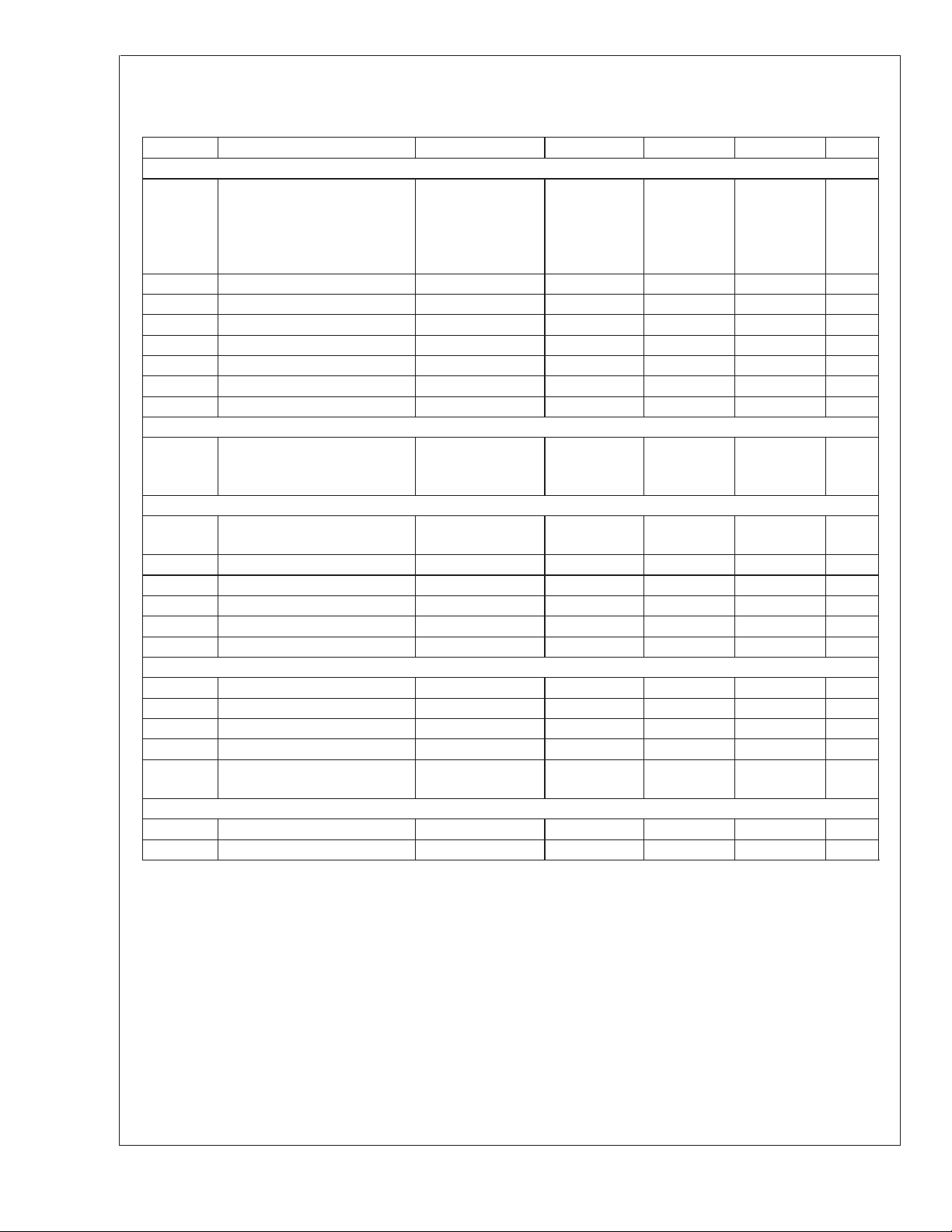
Electrical Characteristics Specifications in standard type face are for T
type apply over the full Operating Junction Temperature Range. Unless otherwise specified: V
VIN Voltage (Note 5) 8V to 30V
Junction Temperature -40˚C to +125˚C
= +25˚C and those in boldface
J
= 15V, RT= 44.2KΩ.
IN
(Note 3)
Symbol Parameter Conditions Min Typ Max Unit
STARTUP CIRCUIT
Start Up Current Before VCC Enable 18 25 µA
VCC Regulator enable threshold 17 20 23 V
VCC Regulator disable
7.25 V
threshold
VIN ESD Clamp voltage I = 5mA 30 36 40 V
I
VIN
Operating supply current COMP = 0VDC 2.5 3.75 mA
VCC SUPPLY
Controller enable threshold 6.5 7 7.5 V
Controller disable threshold 5.3 5.8 6.3 V
VCC regulated output No External Load 8 8.5 9 V
VCC dropout voltage (VIN -
I=5mA 1.7 V
VCC)
VCC regulator current limit VCC = 7.5V (Note
15 22 mA
4)
SKIP CYCLE MODE COMPARATOR
Skip Cycle mode enable
1
⁄3[COMP - 1.25V] 75 125 175 mV
threshold
Skip Cycle mode hysteresis 5 mV
CURRENT LIMIT
CS limit to OUT delay CS stepped from 0
35 ns
to 0.6V, time to OUT
transition low, C
load
=0.
CS limit threshold 0.45 0.5 0.55 V
Leading Edge Blanking time 90 ns
CS blanking sinking impedance 35 55 Ω
SOFT-START
V
SS-OCV
SS pin open-circuit voltage 4.3 5.2 6.1 V
Soft-start Current Source 15 22 30 µA
Soft-start to COMP Offset 0.35 0.55 0.75 V
COMP sinking impedance During SS ramp 60 Ω
OSCILLATOR
Frequency1 (RT = 44.2K) 135 150 165 kHz
Frequency2 (RT = 13.3K) 440 500 560 kHz
Sync threshold 2.4 3.2 3.8 V
www.national.com3
Electrical Characteristics Specifications in standard type face are for T
apply over the full Operating Junction Temperature Range. Unless otherwise specified: V
LM5021
3) (Continued)
= +25˚C and those in boldface type
J
= 15V, RT= 44.2KΩ. (Note
IN
Symbol Parameter Conditions Min Typ Max Unit
PWM COMPARATOR
COMP to OUT delay COMP set to 2V
20 ns
CS stepped 0 to
0.4V, time to OUT
transition low, C
load
=0.
Min Duty Cycle COMP = 0V 0 %
Max Duty Cycle (-1 Device) 75 80 85 %
Max Duty Cycle (-2 Device) 50 %
COMP to PWM comparator gain 0.33
COMP Open Circuit Voltage 4.2 5.1 6 V
COMP at Max Duty Cycle 2.75 V
COMP Short Circuit Current COMP = 0V 0.6 1.1 1.5 mA
SLOPE COMPENSATION
Slope Comp Amplitude
(LM5021-1 only)
CS pin to PWM
Comparator offset at
70 90 110 mV
maximum duty cycle
OUTPUT SECTION
OUT High Saturation IOUT = 50mA, VCC
0.6 1.1 V
- OUT
OUT Low Saturation IOUT = 100mA 0.3 1 V
Peak Source Current OUT = VCC/2. 0.3 A
Peak Sink Current OUT = VCC/2. 0.7 A
Rise time C
Fall time C
= 1nF 25 ns
load
= 1nF 10 ns
load
HICCUP MODE
V
V
I
I
OVLD
V
RST
DTCS
OVCS
Over load detection threshold COMP pin V
Hiccup mode threshold SS pin V
HIC
SS-OCV
SS-OCV
– 0.8 V
– 0.8 V
SS-OCV
SS-OCV
– 0.6 V
– 0.6 V
SS-OCV
SS-OCV
Hiccup mode Restart threshold SS pin 0.1 0.3 0.5 V
Dead-time current source 0.1 0.25 0.4 µA
Overload detection timer current
6 10 14 µA
– 0.4 V
– 0.4 V
source
THERMAL RESISTANCE
θ
θ
Note 1: Absolute Maximum Ratingsare limitsbeyond which damageto thedevice may occur. Operating Ratingsare conditions underwhich operationof the device
is intended to be functional. For guaranteed specifications and test conditions, see the Electrical Characteristics.
Note 2: The human body model is a 100 pF capacitor discharged through a 1.5kΩ resistor into each pin.
Note 3: Min and Max limits are 100% production tested at 25˚C. Limits over the operating temperature range are guaranteed through correlation using Statistical
Quality Control (SQC) methods. Limits are used to calculate National’s Average Outgoing Quality Level (AOQL).
Note 4: Device thermal limitations may limit usable range.
Note 5: After initial turn-on at VIN = 20V.
MSOP-8 Junction to Ambient 0 LFM 200 ˚C/W
JA
MDIP-8 Junction to Ambient 0 LFM 107 ˚C/W
JA
www.national.com 4

Simplified Block Diagram
LM5021
FIGURE 1.
20144203
www.national.com5

Typical Performance Characteristics Unless otherwise specified: T
LM5021
VIN Start-Up Current VIN UVLO
= 25˚C.
J
20144204
20144205
VIN Current vs OUT Load VIN Voltage Falling vs VCC Voltage
20144206
20144207
OUT Driver Current vs Temperature Hiccup Mode Deadtime vs Softstart Capacitance
20144208
www.national.com 6
20144209

LM5021
Typical Performance Characteristics Unless otherwise specified: T
Output Switching Frequency vs RT
20144210
Detailed Operating Description
START UP CIRCUIT
Referring to Figure 2, the input capacitor C
charged through the start-up resistor Rstart, when the rectified ac input voltage HV is applied. The VIN current consumed by the LM5021 is only 18 µA (nominal) while the
capacitor C
is initially charged to the start-up threshold.
VIN
When the input voltage, VIN reaches the upper VIN UVLO
threshold of 20V, the internal VCC linear regulator is enabled. The VCC regulator will remain on until VIN falls to the
lower UVLO threshold of 7.25V (12.5V hysteresis). When
the VCC regulator is turned on, the external capacitor at the
VCC pin begins to charge. The PWM controller, soft-start
circuit and gate driver are enabled when the VCC voltage
reaches the VCC UVLO upper threshold of 7V. The VCC
UVLO has 1.2V hysteresis between the upper and lower
VIN
is trickle
thresholds to avoid chattering during transients on the VCC
pin. When the VCC UVLO enables the switching power
supply,energy is transferred from the primary to thesecondary transformer winding(s). A bias winding, shown in Figure
2, delivers powerto the VINpin to sustain theVCC regulator.
The voltage supplied should be from 11V (VCC regulated
voltage maximum plus VCC regulator dropout voltage) to
30V (maximum operating VIN voltage). The start-up sequence is completed and normal operation begins when the
voltage from the bias winding is sufficient to maintain VCC
level greater than the VCC UVLO threshold (5.8V typical).
The size of the start-up resistorRstart not only affects power
supply start-up time, but also power supply efficiency since
the resistor dissipates power in normal operation. The ultra
low start-up current of the LM5021 allows a large value
Rstart resistor (up to 3 MΩ) for improved efficiency with
reasonable start-up time.
= 25˚C. (Continued)
J
FIGURE 2. Start-Up Circuit Block Diagram
20144211
www.national.com7

Detailed Operating Description
(Continued)
LM5021
RELATIONSHIP BETWEEN INPUT CAPACITOR C
CAPACITOR C
V
CC
The internal VCC linear regulator is enabled when VIN
reaches 20V. The drop in VIN due to charge transfer from
to C
C
VIN
VCC
from the following equations where VIN’ is the voltage on
immediately after the VCC regulator charges C
C
VIN
Assuming C
drop in VIN will be 0.85V, or the VIN value drops to 19.15V.
The value of the VCC capacitorcan be small (less than 1uF)
as it supplies only transient gate drive current of a short
duration. The C
gate drive current and the quiescent current of LM5021until
the transformer bias winding delivers sufficient voltage to
VIN to sustain the VCC voltage.
The C
capacitor value can be calculated from the operat-
VIN
ing VCC load current after it’s output voltage reaches the
VCC UVLO threshold. For example, if the LM5021 is driving
an external MOSFET with total gate charge (Qg) of 25nC,
the average gate drivecurrent is Qg x Fsw, where Fswis the
switching frequency. Assuming a switching frequency of
150KHz, the averagegate drive currentis 3.75mA. Sincethe
IC consumes approximately 2.5mA operating current in addition to the gate current, the total current drawn from C
capacitor is the operating current plus the gate charge current, or 6.25mA. The C
for a brief time until the transformer bias winding takes over.
The C
voltage must not fallbelow 8.5V during the start-up
VIN
sequence or the cyclewill be restarted. The maximumallowable start-up time can be calculated using the value of C
the change in voltage allow at VIN (19.15V – 8.5V) and the
VCC regulator current (6.25mA). Tmax, the maximum time
allowed to energize the bias winding is:
If the calculated value of Tmax is too small, the value of Cin
should be increased further to allow more time before the
transformer bias winding takes over and delivers the operating current to the VCC regulator. Increasing C
crease the time from theapplication of the rectified ac (HVin
the Figure 2) to the time when VIN reaches the 20V start
threshold. The initial charging time of C
VCC
after the regulatoris enabled can becalculated
∆VINxC
(20V – V
value as 10 µF, and C
VIN
VIN
= ∆VCCxC
VIN
IN’)CVIN
= 8.5V C
VCC
VCC
of 1µF, then the
VCC
capacitor must be sized to supply the
capacitor must supply this current
VIN
is:
VIN
VIN
&
IN
VCC
will in-
.
VIN
VIN
PWM COMPARATOR/SLOPE COMPENSATION
The PWM comparator compares the current sense signal
with the loop error voltage from the COMP pin. The COMP
pin voltage is reduced by 1.25V then attenuated by a 3:1
resistor divider. The PWM comparator input offset voltage is
designed such that less than 1.25V at the COMP pin will
result in a zero duty cycle at the controller output.
For duty cycles greater than 50 percent, current mode control circuits are subject to sub-harmonic oscillation. By adding an additional fixed slope voltage ramp signal (slope
compensation) to the current sense signal, this oscillation
can be avoided. The LM5021-1 integrates this slope compensation by summing a ramp signal generated by the oscillator with the current sense signal. The slope compensation is generated by a current ramp driven through an
internal 1.8 kΩ resistor connected to the CS pin. Additional
slope compensation may be added by increasing the resistance between the current sense filter capacitor and the CS
pin, thereby increasing the voltage ramp created by the
oscillator currentramp. Since theLM5021-2 is notcapable of
duty cycles greater than 50%, there is no slope compensation feature in this device.
CURRENT LIMIT/CURRENT SENSE
The LM5021 provides a cycle-by-cycle over current protection feature. Current limit is triggered by an internal current
sense comparator threshold which isset at 500mV. If the CS
pin voltage plus the slope compensation voltage exceeds
500mV, the OUT pin output pulse will be immediately terminated.
An RC filter, located near the LM5021, is recommended for
the CS pin to attenuate the noise coupled from the power
FET’s gate to source. The CS pin capacitance is discharged
at the end of each PWM clock cycle by an internal switch.
The discharge switch remains on for an additional 90ns
leading edge blanking intervalto attenuate the currentsense
transient that occurs when the external power FET is turned
on. In addition to providingleading edge blanking, this circuit
also improves dynamic performance by discharging the current sense filter capacitor at the conclusion of every cycle.
The LM5021 CS comparator is very fast, and may respond
to short duration noise pulses. Layout considerations are
critical for the current sense filter and sense resistor. The
,
capacitor associated with the CS filter must be placed very
close to the device and connected directly to the pins of the
IC (CS and GND). If a current sense transformer is used,
both leads of the transformer secondary should be routed to
the sense resistor, which should also be located close to the
IC. If a current sense resistor located in the power FET’s
source is used forcurrent sense, a low inductance resistoris
required. In this case, all of the noise sensitive low current
grounds should be connected in common near the IC and
then a single connection should be made to the power
ground (sense resistor ground point).
OSCILLATOR, SHUTDOWN and SYNC CAPABILITY
A single external resistor connected between RT and GND
pins sets the LM5021 oscillator frequency. The LM5021-2
device, with 50% maximum duty cycle, includes an internal
flip-flop that divides the oscillator frequency by two. This
method produces a precise 50% maximum duty cycle limit.
Because of this frequency divider,the oscillator frequency of
the LM5021-2 is actually twice the frequency of the gate
drive output (OUT). For the LM5021-1 device, the oscillator
www.national.com 8

Detailed Operating Description
(Continued)
frequency and the operational output frequency are the
same. Toset a desiredoutput switching frequency (Fsw),the
RT resistor can be calculated from:
LM5021-1:
LM5021-2:
The LM5021 can also be synchronized to an external clock.
The external clock must have a higher frequency than the
free running oscillator frequency set by the RT resistor. The
clock signal should be capacitively coupled into the RT pin
with a 100pF capacitor. Apeak voltage levelgreater than 3.8
Voltsat the RTpin is required fordetection of the syncpulse.
The dc voltage across the RT resistor is internally regulated
at 2 volts. Therefore, the ac pulse superimposed on the RT
resistor must have 1.8V or greater amplitude to successfully
synchronize the oscillator. The sync pulse width should be
set between 15ns to150ns by the external components.The
RT resistor is always required, whether the oscillator is free
running or externally synchronized. The RT resistor should
be located very close to thedevice and connected directly to
the pins of the LM5021 (RT and GND).
GATE DRIVER and MAX DUTY CYCLE LIMIT
The LM5021 providesa gate driver (OUT),which can source
peak current of 0.3Aand sink 0.7A. The LM5021 is available
in two duty-cycle limit options. The maximum output dutycycle is typically 80% forthe LM5021-1 option, and precisely
equal to 50% for the LM5021-2 option. The maximum duty
cycle function for the LM5021-2 is accomplished with an
internal toggle flip-flop toensure an accurate duty cyclelimit.
The internal oscillator frequency of the LM5021-2 is therefore twice the switching frequency of the PWM controller
(OUT pin).
The 80% maximum duty-cycle function for the LM5021-1 is
determined by the internal oscillator. For the LM5021-1 the
internal oscillator frequency and the switching frequency of
the PWM controller are the same.
SOFT-START
The soft-start featureallows thepower converter togradually
reach the initial steady state operating point, thus reducing
start-up stresses and current surges. An internal 22 µA
current source charges an external capacitor connected to
the SS pin.The capacitor voltagewill ramp upslowly, limiting
the COMP pin voltage and the duty cycle of the output
pulses. The soft-start capacitor is also used to generate the
hiccup mode delay time when the output of the switching
power supply is continuously overloaded.
HICCUP MODE OVERLOAD CURRENT LIMITING
Hiccup mode is a method of protecting the power supply
from over-heating and damage during an extended overload
condition. When the output fault is removed the power supply will automatically restart.
Figure 3, Figure 4 and Figure 5 illustrate the equivalent
circuit of the hiccup mode for LM5021 and the relevant
waveforms. During start-up and in normal operation, the
external soft-start capacitor Css is pulled up by a current
source that delivers 22 µA to the SS pin capacitor. In normal
operation, the soft-start capacitor continues to charge and
eventually reaches the saturation voltage of the current
source (V
, nominally 5.2V). During start-up the
SS_OCV
COMP pin voltage follows the SS capacitor voltage and
gradually increases the peak current delivered by the power
supply. When the output of the switching power supply
reaches the desired voltage, the voltage feedback amplifier
takes control of the COMP signal (via the opto-coupler). In
normal operation the COMP level is held at an intermediate
voltage between 1.25V and 2.75V controlled by the voltage
regulation loop. When the COMPpin voltage is below 1.25V,
the duty-cycle iszero. When the COMPlevel is above2.75V,
the duty cycle will be limited by the 0.5V threshold of cycleby-cycle current limit comparator.
If the output of the power supply is overloaded, the voltage
regulation loop demands more current by increasing the
COMP pin control voltage.When the COMP pin exceedsthe
over voltage detection threshold (V
, nominally 4.6V),
OVLD
the SS capacitor Css will be discharged by a 10µA overload
detection timer current source, I
above V
long enough for the SS capacitor to discharge
OVLD
to the Hiccup mode threshold (V
. If COMP remains
OVCS
, nominally 4.6V), the
HIC
controller enters the hiccup mode. The OUT pin is then
latched low andthe SS capacitor dischargecurrent source is
reduced from 10 µA to 0.25 µA, the dead-time current
source, I
reaches the Restart threshold (V
. The SS pin voltage is slowly reduced until it
DTCS
, nominally 0.3V). Then
RST
a new start-up sequence commences with 22 µA current
source charging the capacitor C
. The slow discharge of
SS
the SS capacitor from the Hiccup threshold to the Restart
threshold provides an extended off time that reduces the
overheating of components including diodes and MOSFETs
due to the continuous overload. The off time during the
hiccup mode can be calculated from the following equation:
Example:
Toff = 808ms, assuming the C
capacitor value is 0.047 µF
SS
Short duration intermittent overloads will not trigger the hiccup mode. The overload duration required to trigger the
hiccup response is set by the capacitor C
, the 10 µA
SS
discharge current sourceand voltage differencebetween the
saturation level of the SS pin and the Hiccup mode threshold. Figure 5 shows the waveform of SS pin with a short
duration overload condition. The overload time required to
enter the hiccup mode can be calculated from the following
equation:
Example:
Toverload = 2.82 ms, assuming the C
capacitor value is
SS
0.047 µF
LM5021
www.national.com9

Detailed Operating Description (Continued)
LM5021
FIGURE 3. Hiccup Mode Control
FIGURE 4. Waveform at SS and COMP Pin due to Continuous Overload
20144219
20144220
www.national.com 10

Detailed Operating Description (Continued)
FIGURE 5. Waveform at SS and COMP Pin due to Brief Overload
LM5021
20144221
SKIP CYCLE OPERATION
During light load conditions, the efficiency of the switching
power supply typically drops as the losses associated with
switching and operating bias currents of the converter become a significant percentage of the power delivered to the
load. The largest component of the power loss is the switching loss associated with the gate driver and external MOSFET gate charge. Each PWM cycle consumes afinite amout
of energy as the MOSFET is turned on and then turned off.
These switching losses are proportional to the frequency of
operation. The Skip Cycle function integrated within the
LM5021 controller reduces the average switching frequency
to reduce switching losses and improve efficiency during
light load conditions.
When a light load condition occurs, the COMP pin voltage is
reduced by the voltage feedback loop to reduce the peak
current delivered by the controller. Referring to Figure 6, the
PWM comparator inputtracks the COMPpin voltagethrough
a 1.25V level shift circuit and a 3:1 resistor divider. As the
COMP pin voltage falls, the input to the PWM comparator
falls proportionately. When the PWM comparator input falls
to 125mV, the Skip Cycle comparator detects the light load
condition and disables output pulses from the controller. The
controller continues to skip switching cycles until the power
supply output falls and the COMP pin voltage increases to
demand more output current. The number of cycles skipped
will depend on the load and the response time of the frequency compensation network. Eventually the COMP voltage will increase when the voltage loop requires more current to sustain the regulated output voltage. When the PWM
comparator input exceeds 130mV (5mV hysteresis), normal
fixed frequency switching resumes. Typical power supply
designs will produce a short burst of output pulses followed
by a long skip cycle interval. The average switching frequency in the Skip Cyclemode can be a small fraction ofthe
normal operating frequency of the power supply.
www.national.com11

Detailed Operating Description (Continued)
LM5021
FIGURE 6. Skip Cycle Control
20144222
www.national.com 12

20144223
LM5021
Typical Application Circuit
www.national.com13

Physical Dimensions inches (millimeters)
unless otherwise noted
LM5021
8 Lead MSOP Package
NS Package Number MUA08A
8 Lead MDIP Package
NS Package Number N08E
www.national.com 14

Notes
LM5021 AC-DC Current Mode PWM Controller
National does not assume any responsibility for use of any circuitry described, no circuit patent licenses are implied and National reserves
the right at any time without notice to change said circuitry and specifications.
For the most current product information visit us at www.national.com.
LIFE SUPPORT POLICY
NATIONAL’S PRODUCTS ARE NOT AUTHORIZED FOR USE AS CRITICAL COMPONENTS IN LIFE SUPPORT DEVICES OR SYSTEMS
WITHOUT THE EXPRESS WRITTEN APPROVAL OF THE PRESIDENT AND GENERAL COUNSEL OF NATIONAL SEMICONDUCTOR
CORPORATION. As used herein:
1. Life support devices or systems are devices or systems
which, (a) are intended for surgical implant into the body, or
(b) support or sustain life, and whose failure to perform when
properly used in accordance with instructions for use
2. A critical component is any component of a life support
device or system whose failure to perform can be reasonably
expected to cause the failure of the life support device or
system, or to affect its safety or effectiveness.
provided in the labeling, can be reasonably expected to result
in a significant injury to the user.
BANNED SUBSTANCE COMPLIANCE
National Semiconductor manufactures products and uses packing materials that meet the provisions of the Customer Products
Stewardship Specification (CSP-9-111C2) and the Banned Substances and Materials of Interest Specification (CSP-9-111S2) and contain
no ‘‘Banned Substances’’ as defined in CSP-9-111S2.
Leadfree products are RoHS compliant.
National Semiconductor
Americas Customer
Support Center
Email: new.feedback@nsc.com
Tel: 1-800-272-9959
www.national.com
National Semiconductor
Europe Customer Support Center
Fax: +49 (0) 180-530 85 86
Email: europe.support@nsc.com
Deutsch Tel: +49 (0) 69 9508 6208
English Tel: +44 (0) 870 24 0 2171
Français Tel: +33 (0) 1 41 91 8790
National Semiconductor
Asia Pacific Customer
Support Center
Email: ap.support@nsc.com
National Semiconductor
Japan Customer Support Center
Fax: 81-3-5639-7507
Email: jpn.feedback@nsc.com
Tel: 81-3-5639-7560
 Loading...