

LM5010A
High Voltage 1A Step Down Switching Regulator
LM5010A High Voltage 1A Step Down Switching Regulator
January 25, 2008
General Description
The LM5010A Step Down Switching Regulator is an enhanced version of the LM5010 with the input operating range
extended to 6V minimum. The LM5010A features all the functions needed to implement a low cost, efficient, buck regulator
capable of supplying in excess of 1A load current. This high
voltage regulator integrates an N-Channel Buck Switch, and
is available in thermally enhanced LLP-10 and TSSOP-14EP
packages. The constant on-time regulation scheme requires
no loop compensation resulting in fast load transient response and simplified circuit implementation. The operating
frequency remains constant with line and load variations due
to the inverse relationship between the input voltage and the
on-time. The valley current limit detection is set at 1.25A. Additional features include: VCC under-voltage lock-out, thermal
shutdown, gate drive under-voltage lock-out, and maximum
duty cycle limiter.
Features
Wide 6V to 75V Input Voltage Range
■
Valley Current Limiting At 1.25A
■
Programmable Switching Frequency Up To 1 MHz
■
Integrated 80V N-Channel Buck Switch
■
Integrated High Voltage Bias Regulator
■
No Loop Compensation Required
■
Ultra-Fast Transient Response
■
Nearly Constant Operating Frequency With Line and Load
■
Variations
Adjustable Output Voltage
■
2.5V, ±2% Feedback Reference
■
Programmable Soft-Start
■
Thermal shutdown
■
Typical Applications
Non-Isolated Telecommunications Regulator
■
Secondary Side Post Regulator
■
Power Supply for Automotive Electronics
■
Package
LLP-10 (4 mm x 4 mm)
■
TSSOP-14EP
■
Both Packages Have Exposed Thermal Pad For Improved
■
Heat Dissipation
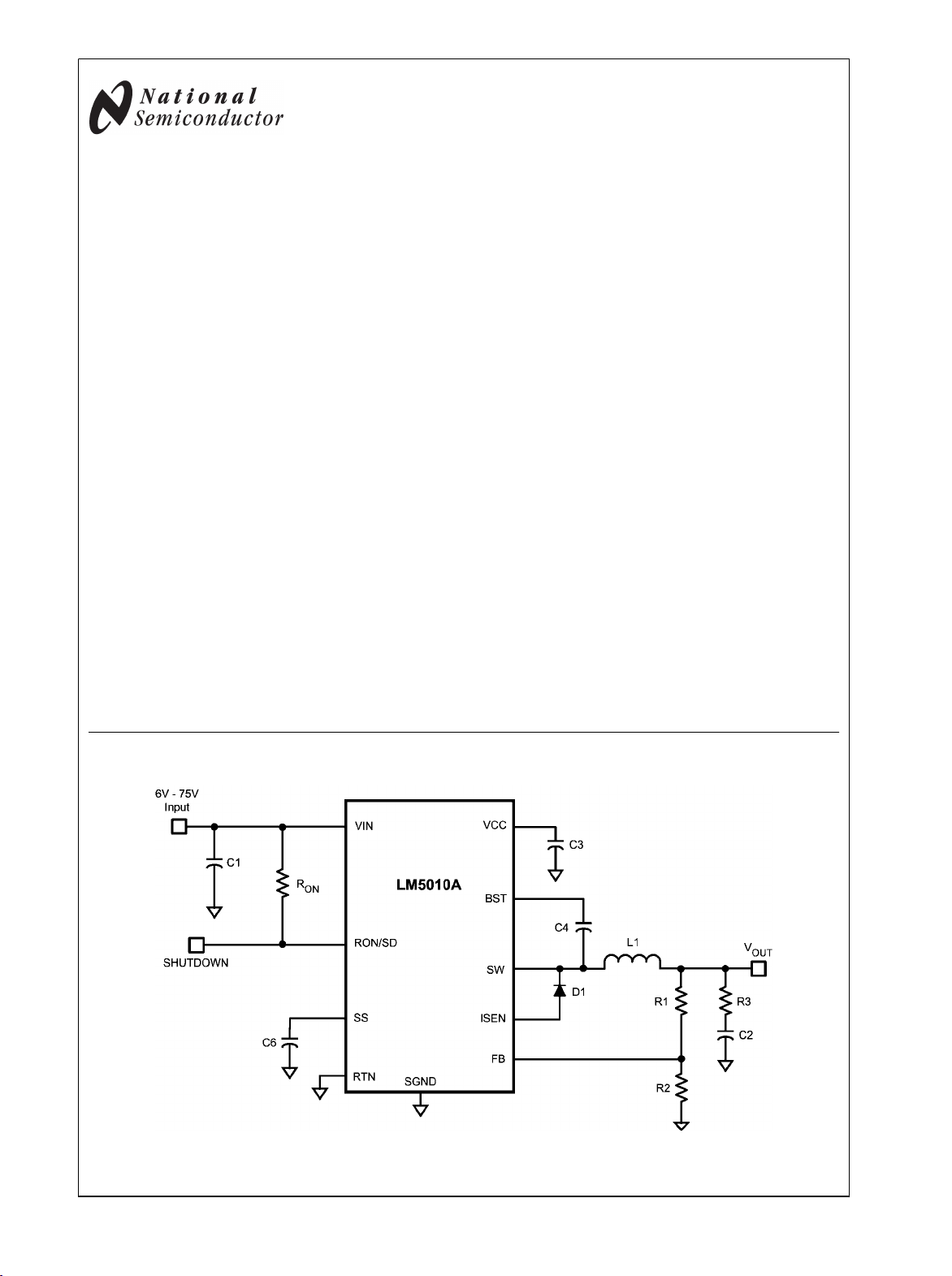
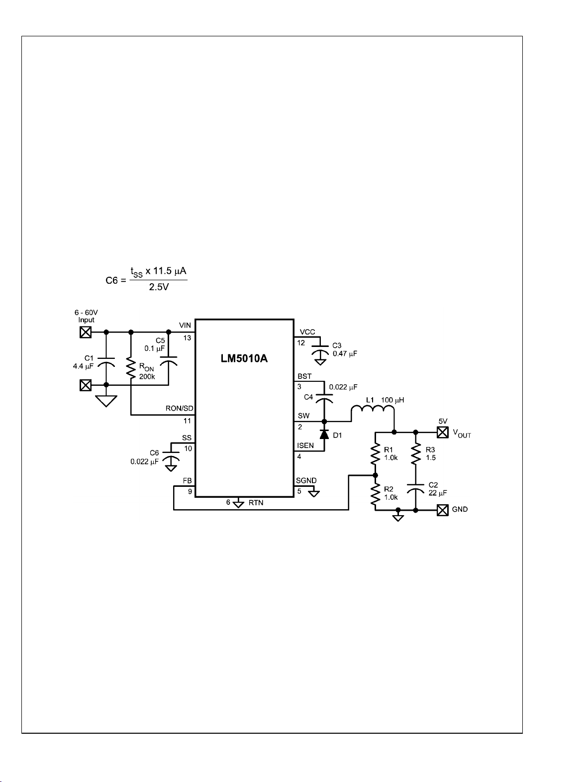
Basic Step Down Regulator
20153843
© 2008 National Semiconductor Corporation 201538 www.national.com
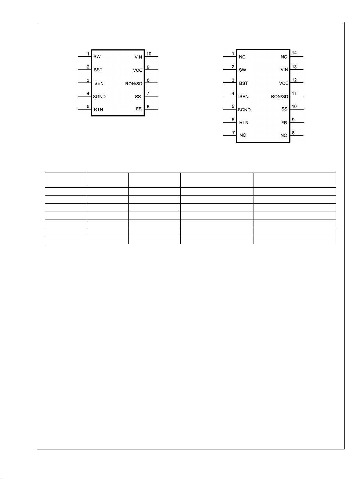
Connection Diagrams
LM5010A
Ordering Information
20153802
20153803
Order Number Package Type NSC Package
Drawing
LM5010ASD LLP-10 (4x4) SDC10A −40°C to + 125°C 1000 Units on Tape and Reel
LM5010ASDX LLP-10 (4x4) SDC10A −40°C to + 125°C 4500 Units on Tape and Reel
LM5010AMH TSSOP-14EP MXA14A −40°C to + 125°C 94 Units in Rail
LM5010AMHE TSSOP-14EP MXA14A −40°C to + 125°C 250 Units on Tape and Reel
LM5010AMHX TSSOP-14EP MXA14A −40°C to + 125°C 2500 Units on Tape and Reel
LM5010AHMH TSSOP-14EP MXA14A −40°C to + 150°C Available Soon
LM5010AHMHX TSSOP-14EP MXA14A −40°C to + 150°C Available Soon
Junction Temperature Range Supplied As
www.national.com 2
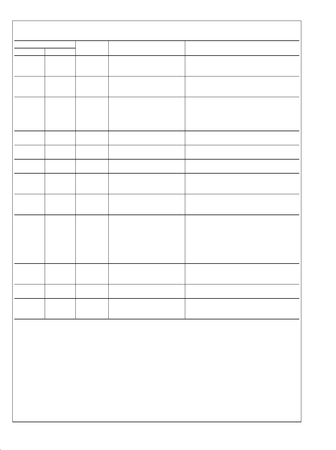
Pin Descriptions
Pin Number Name Description Application Information
LLP-10 TSSOP-14
1 2 SW Switching Node Internally connected to the buck switch source.
Connect to the inductor, free-wheeling diode, and
bootstrap capacitor.
2 3 BST Boost pin for bootstrap capacitor Connect a capacitor from SW to the BST pin. The
capacitor is charged from VCC via an internal diode
during the buck switch off-time.
3 4 ISEN Current sense During the buck switch off-time, the inductor current
flows through the internal sense resistor, and out of
the ISEN pin to the free-wheeling diode. The current
limit comparator keeps the buck switch off if the ISEN
current exceeds 1.25A (typical).
4 5 SGND Current Sense Ground Re-circulating current flows into this pin to the current
sense resistor.
5 6 RTN Circuit Ground Ground return for all internal circuitry other than the
current sense resistor.
6 9 FB Voltage feedback input from the
regulated output
7 10 SS Softstart An internal 11.5 µA current source charges the SS pin
8 11 RON/SD On-time control and shutdown An external resistor from VIN to the RON/SD pin sets
9 12 VCC Output of the bias regulator The voltage at VCC is nominally equal to VIN for V
10 13 VIN Input supply voltage Nominal input range is 6V to 75V. Input bypass
1,7,8,14 NC No connection. No internal connection. Can be connected to ground
EP Exposed Pad Exposed metal pad on the underside of the device. It
Input to both the regulation and over-voltage
comparators. The FB pin regulation level is 2.5V.
capacitor to 2.5V to soft-start the reference input of
the regulation comparator.
the buck switch on-time. Grounding this pin shuts
down the regulator.
< 8.9V, and regulated at 7V for VIN > 8.9V. Connect
a 0.47 µF, or larger capacitor from VCC to ground, as
close as possible to the pins. An external voltage can
be applied to this pin to reduce internal dissipation if
VIN is greater than 8.9V. MOSFET body diodes clamp
VCC to VIN if VCC > VIN.
capacitors should be located as close as possible to
the VIN pin and RTN pins.
plane to improve heat dissipation.
is recommended to connect this pad to the PC board
ground plane to aid in heat dissipation.
LM5010A
IN
3 www.national.com
Absolute Maximum Ratings (Note 1)
If Military/Aerospace specified devices are required,
please contact the National Semiconductor Sales Office/
LM5010A
Distributors for availability and specifications.
VIN to RTN -0.3V to 76V
BST to RTN -0.3V to 90V
SW to RTN (Steady State) -1.5V
BST to VCC 76V
BST to SW 14V
VCC to RTN -0.3V to 14V
SGND to RTN -0.3V to +0.3V
SS to RTN -0.3V to 4V
VIN to SW 76V
All Other Inputs to RTN -0.3V to 7V
ESD Rating (Note 2)
Human Body Model 2kV
Storage Temperature Range -65°C to +150°C
Lead Temperature (Soldering 4 sec) (Note 4) 260°C
Operating Ratings (Note 1)
VIN Voltage 6.0V to 75V
Junction Temperature
LM5010A −40°C to + 125°C
LM5010AH −40°C to + 150°C
Electrical Charateristics Specifications with standard type are for T
= 25°C only; limits in boldface type apply
J
over the full Operating Junction Temperature (TJ) range. Minimum and Maximum limits are guaranteed through test, design, or
statistical correlation. Typical values represent the most likely parametric norm at TJ = 25°C, and are provided for reference
purposes only. Unless otherwise stated the following conditions apply: VIN = 48V, RON = 200kΩ. See (Note 5).
Symbol Parameter Conditions Min Typ Max Units
VCC Regulator
VCCReg VCC regulated output 6.6 7 7.4 Volts
VIN - V
CC
ICC = 0 mA, FS < 200 kHz, 6.0V ≤ VIN ≤ 8.5V
100 mV
VCC Bypass Threshold VIN Increasing 8.9 V
VCC Bypass Hysteresis VIN Decreasing 260 mV
VCC output impedance
VIN = 8.0V 50
(0 mA ≤ ICC ≤ 5 mA)
VIN = 6.0V 55
Ω
VIN = 48V 0.21
VCC current limit (Note 3) VIN = 48V, VCC = 0V 15 mA
UVLOVcc VCC under-voltage lock-out
VCC Increasing 5.25 V
threshold
UVLO
UVLO
hysteresis VCC Decreasing 180 mV
VCC
filter delay 100 mV overdrive 3 µs
VCC
IIN operating current Non-switching, FB = 3V 675 950 µA
IIN shutdown current RON/SD = 0V 100 200 µA
Switch Characteristics
R
DS(on)
UVLO
Buck Switch R
DS(on)
200 mA
Gate Drive UVLO V
GD
@ ISW =
TJ ≤ 125°C
TJ ≤ 150°C
- VSW Increasing 1.7 3.0 4.0 V
BST
0.35 0.80
0.85
Ω
UVLOGD hysteresis 400 mV
SOFT-START Pin
I
SS
Internal current source 8.0 11.5 15 µA
Current Limit
I
LIM
Resistance from ISEN to SGND 130
Threshold Current out of I
SEN
1 1.25 1.5 A
mΩ
Response time 150 ns
On Timer, RON/SD Pin
tON - 1 On-time
tON - 2 On-time
VIN = 10V, RON = 200 kΩ
VIN = 75V, RON = 200 kΩ
2.1 2.75 3.4 µs
290 390 496 ns
Shutdown threshold Voltage at RON/SD rising 0.30 0.7 1.05 V
Threshold hysteresis 40 mV
www.national.com 4
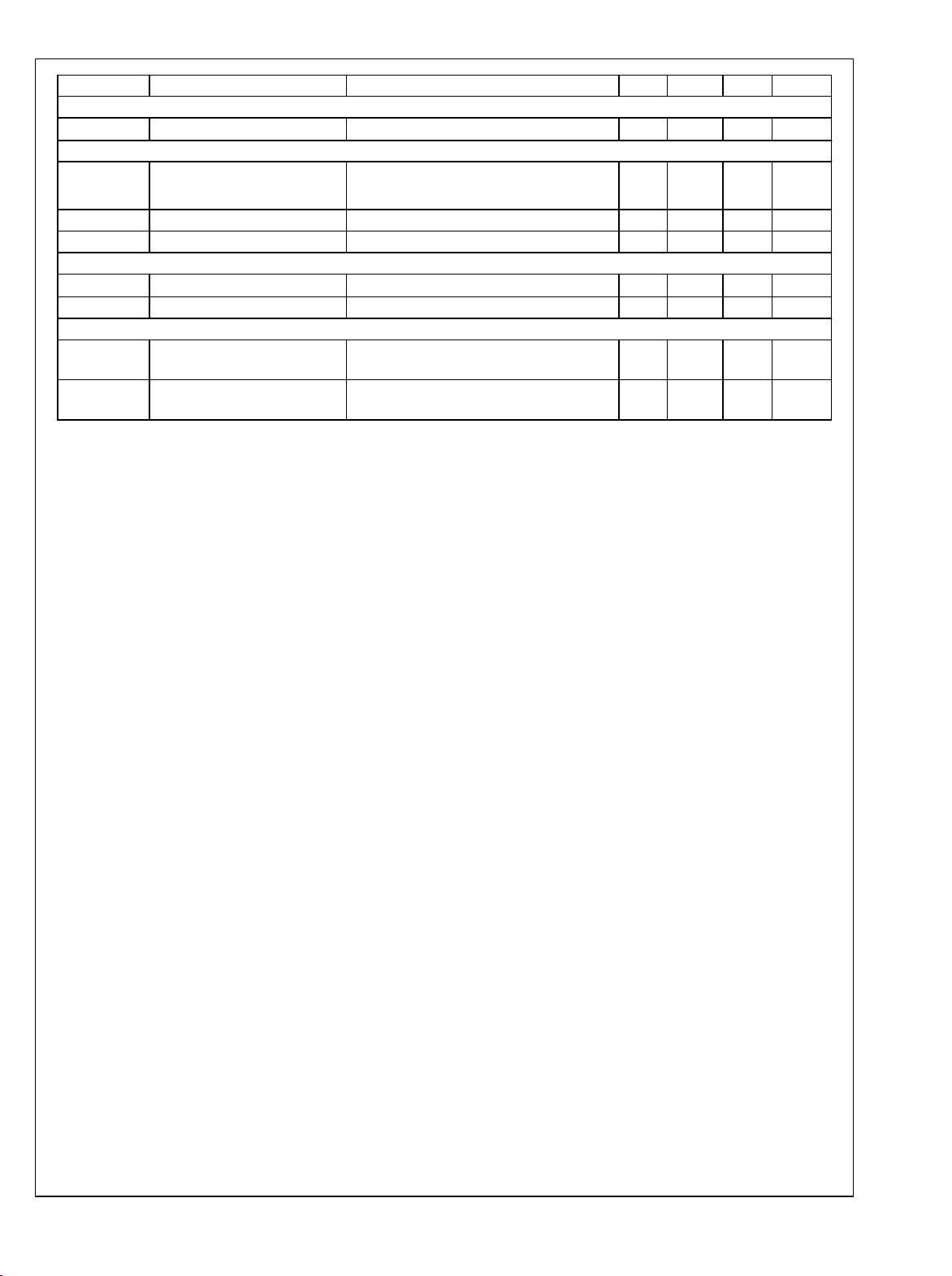
Symbol Parameter Conditions Min Typ Max Units
Off Timer
t
OFF
Minimum Off-time 260 ns
Regulation and Over-Voltage Comparators (FB Pin)
V
REF
FB regulation threshold
TJ ≤ 125°C
TJ ≤ 150°C
2.445
2.435
2.50 2.550 V
FB over-voltage threshold 2.9 V
FB bias current 1 nA
Thermal Shutdown
T
SD
Thermal shutdown temperature 175 °C
Thermal shutdown hysteresis 20 °C
Thermal Resistance
θ
JA
Junction to Ambient, 0 LFPM Air
Flow
θ
JC
Note 1: Absolute Maximum Ratings are limits beyond which damage to the device may occur. Operating Ratings are conditions under which operation of the
device is intended to be functional. For guaranteed specifications and test conditions, see the Electrical Characteristics.
Note 2: The human body model is a 100pF capacitor discharged through a 1.5kΩ resistor into each pin.
Note 3: VCC provides bias for the internal gate drive and control circuits. Device thermal limitations limit external loading.
Note 4: For detailed information on soldering plastic TSSOP and LLP packages refer to the Packaging Data Book available from National Semiconductor
Corporation.
Note 5: Typical specifications represent the most likely parametric norm at 25°C operation.
Junction to Case SDC Package
SDC Package
MXA Package
MXA Package
40
40
5.2
5.2
°C/W
°C/W
LM5010A
5 www.national.com
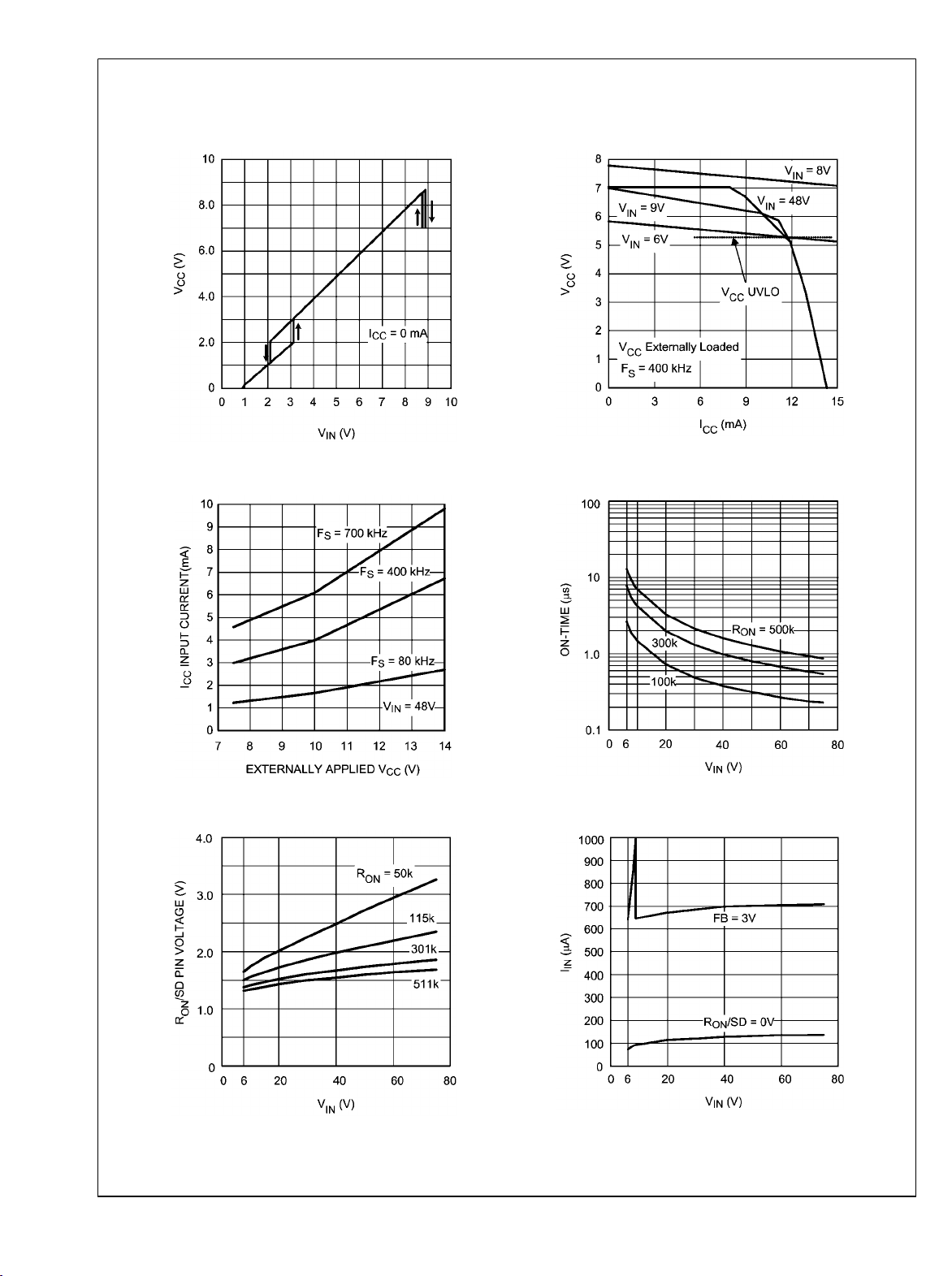
Typical Performance Characteristics
LM5010A
VCC vs V
IN
ICC vs Externally Applied V
CC
20153804
VCC vs I
CC
On-Time vs VIN and R
20153805
ON
20153806
Voltage at RON/SD Pin
20153808
www.national.com 6
IIN vs V
20153807
IN
20153810

Block Diagram
LM5010A
20153844
7 www.national.com

LM5010A
FIGURE 1. Startup Sequence
Functional Description
The LM5010A Step Down Switching Regulator features all
the functions needed to implement a low cost, efficient buck
DC-DC converter capable of supplying in excess of 1A to the
load. This high voltage regulator integrates an 80V N-Channel
buck switch, with an easy to implement constant on-time controller. It is available in the thermally enhanced LLP-10 and
TSSOP-14EP packages. The regulator compares the feedback voltage to a 2.5V reference to control the buck switch,
and provides a switch on-time which varies inversely with VIN.
This feature results in the operating frequency remaining relatively constant with load and input voltage variations. The
switching frequency can range from less than 100 kHz to 1.0
MHz. The regulator requires no loop compensation resulting
in very fast load transient response. The valley current limit
circuit holds the buck switch off until the free-wheeling inductor current falls below the current limit threshold, nominally set
at 1.25A.
The LM5010A can be applied in numerous applications to efficiently step down higher DC voltages. This regulator is well
www.national.com 8
20153811
suited for 48V telecom applications, as well as the 42V automotive power bus. Features include: Thermal shutdown, VCC
under-voltage lock-out, gate drive under-voltage lock-out, and
maximum duty cycle limit.
Control Circuit Overview
The LM5010A employs a control scheme based on a comparator and a one-shot on-timer, with the output voltage feedback (FB) compared to an internal reference (2.5V). If the FB
voltage is below the reference the buck switch is turned on for
a time period determined by the input voltage and a programming resistor (RON). Following the on-time the switch remains
off for a fixed 260 ns off-time, or until the FB voltage falls below
the reference, whichever is longer. The buck switch then turns
on for another on-time period. Referring to the Block Diagram,
the output voltage is set by R1 and R2. The regulated output
voltage is calculated as follows:
V
= 2.5V x (R1 + R2) / R2 (1)
OUT
The LM5010A requires a minimum of 25 mV of ripple voltage
at the FB pin for stable fixed-frequency operation. If the output

LM5010A
capacitor’s ESR is insufficient additional series resistance
may be required (R3 in the Block Diagram).
The LM5010A operates in continuous conduction mode at
heavy load currents, and discontinuous conduction mode at
light load currents. In continuous conduction mode current always flows through the inductor, never decaying to zero
during the off-time. In this mode the operating frequency remains relatively constant with load and line variations. The
minimum load current for continuous conduction mode is onehalf the inductor’s ripple current amplitude. The operating
frequency in the continuous conduction mode is calculated as
follows:
(2)
The buck switch duty cycle is equal to:
(3)
Under light load conditions, the LM5010A operates in discontinuous conduction mode, with zero current flowing through
the inductor for a portion of the off-time. The operating frequency is always lower than that of the continuous conduction
mode, and the switching frequency varies with load current.
Conversion efficiency is maintained at a relatively high level
at light loads since the switching losses diminish as the power
delivered to the load is reduced. The discontinuous mode operating frequency is approximately:
(4)
where RL = the load resistance.
Start-Up Bias Regulator (VCC)
A high voltage bias regulator is integrated within the
LM5010A. The input pin (VIN) can be connected directly to
line voltages between 6V and 75V. Referring to the block diagram and the graph of VCC vs. VIN, when VIN is between 6V
and the bypass threshold (nominally 8.9V), the bypass switch
(Q2) is on, and VCC tracks VIN within 100 mV to 150 mV. The
bypass switch on-resistance is approximately 50Ω, with inherent current limiting at approximately 100 mA. When VIN is
above the bypass threshold, Q2 is turned off, and VCC is regulated at 7V. The VCC regulator output current is limited at
approximately 15 mA. When the LM5010A is shutdown using
the RON/SD pin, the VCC bypass switch is shut off, regardless
of the voltage at VIN.
When VIN exceeds the bypass threshold, the time required for
Q2 to shut off is approximately 2 - 3 µs. The capacitor at VCC
(C3) must be a minimum of 0.47 µF to prevent the voltage at
VCC from rising above its absolute maximum rating in response to a step input applied at VIN. C3 must be located as
close as possible to the LM5010A pins.
In applications with a relatively high input voltage, power dissipation in the bias regulator is a concern. An auxiliary voltage
of between 7.5V and 14V can be diode connected to the VCC
pin (D2 in Figure 2) to shut off the VCC regulator, reducing
internal power dissipation. The current required into the VCC
pin is shown in the Typical Performance Characteristics. Internally a diode connects VCC to VIN requiring that the auxiliary voltage be less than VIN.
The turn-on sequence is shown in Figure 1. When VCC exceeds the under-voltage lock-out threshold (UVLO) of 5.25V
(t1 in Figure 1), the buck switch is enabled, and the SS pin is
released to allow the soft-start capacitor (C6) to charge up.
The output voltage V
increases to the desired value as the soft-start voltage increases (t2 in Figure 1).
is regulated at a reduced level which
OUT
FIGURE 2. Self Biased Configuration
Regulation Comparator
The feedback voltage at the FB pin is compared to the voltage
at the SS pin (2.5V, ±2%). In normal operation an on-time
period is initiated when the voltage at FB falls below 2.5V. The
buck switch conducts for the on-time programmed by RON,
causing the FB voltage to rise above 2.5V. After the on-time
period the buck switch remains off until the FB voltage falls
20153816
below 2.5V. Input bias current at the FB pin is less than 5 nA
over temperature.
Over-Voltage Comparator
The feedback voltage at FB is compared to an internal 2.9V
reference. If the voltage at FB rises above 2.9V the on-time
is immediately terminated. This condition can occur if the in-
9 www.national.com
put voltage, or the output load, changes suddenly. The buck
switch remains off until the voltage at FB falls below 2.5V.
LM5010A
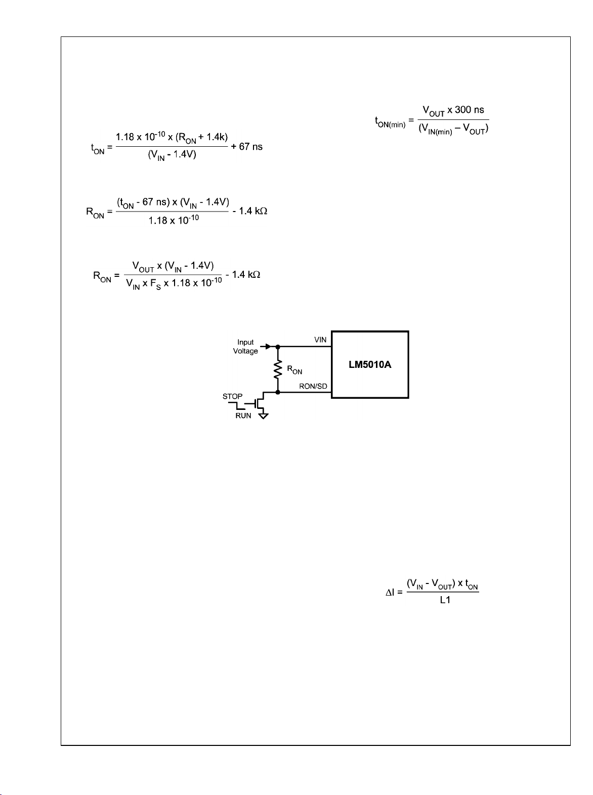
ON-Time Control
The on-time of the internal buck switch is determined by the
RON resistor and the input voltage (VIN), and is calculated as
follows:
the minimum off-time of the LM5010A (260 ns, ±15%). The
fixed off-time limits the maximum duty cycle achievable with
a low voltage at VIN. The minimum allowed on-time to regulate the desired V
the following:
at the minimum VIN is determined from
OUT
(8)
(5)
The RON resistor can be determined from the desired on-time
by re-arranging Equation 5 to the following:
(6)
To set a specific continuous conduction mode switching frequency (Fs), the RON resistor is determined from the following:
(7)
In high frequency applications the minimum value for tON is
limited by the maximum duty cycle required for regulation and
FIGURE 3. Shutdown Implementation
Shutdown
The LM5010A can be remotely shut down by forcing the RON/
SD pin below 0.7V with a switch or open drain device. See
Figure 3. In the shutdown mode the SS pin is internally
grounded, the on-time one-shot is disabled, the input current
at VIN is reduced, and the VCC bypass switch is turned off.
The VCC regulator is not disabled in the shutdown mode. Releasing the RON/SD pin allows normal operation to resume.
The nominal voltage at RON/SD is shown in the Typical Performance Characteristics. When switching the RON/SD pin,
the transition time should be faster than one to two cycles of
the regulator’s nominal switching frequency.
20153818
Current Limit
Current limit detection occurs during the off-time by monitoring the recirculating current through the internal current sense
resistor (R
Referring to the Block Diagram, if the current into SGND during the off-time exceeds the threshold level the current limit
comparator delays the start of the next on-time period. The
next on-time starts when the current into SGND is below the
threshold and the voltage at FB is below 2.5V. Figure 4 illustrates the inductor current waveform during normal operation
and during current limit. The output current IO is the average
of the inductor ripple current waveform. The Low Load Current waveform illustrates continuous conduction mode operation with peak and valley inductor currents below the current
limit threshold. When the load current is increased (High Load
Current), the ripple waveform maintains the same amplitude
and frequency since the current falls below the current limit
threshold at the valley of the ripple waveform. Note the average current in the High Load Current portion of Figure 4 is
above the current limit threshold. Since the current reduces
below the threshold in the normal off-time each cycle, the start
www.national.com 10
). The detection threshold is 1.25A, ±0.25A.
SENSE
of each on-time is not delayed, and the circuit’s output voltage
is regulated at the correct value. When the load current is further increased such that the lower peak would be above the
threshold, the off-time is lengthened to allow the current to
decrease to the threshold before the next on-time begins
(Current Limited portion of Figure 4). Both V
switching frequency are reduced as the circuit operates in a
constant current mode. The load current (I
current limit threshold plus half the ripple current (ΔI/2). The
ripple amplitude (ΔI) is calculated from:
The current limit threshold can be increased by connecting an
external resistor (RCL) between SGND and ISEN. RCL typically is less than 1Ω, and the calculation of its value is explained in the Applications Information section. If the current
limit threshold is increased by adding RCL, the maximum continuous load current should not exceed 1.5A, and the peak
current out of the SW pin should not exceed 2A.
OCL
and the
OUT
) is equal to the
(9)

FIGURE 4. Inductor Current - Current Limit Operation
LM5010A
20153820
N - Channel Buck Switch and Driver
The LM5010A integrates an N-Channel buck switch and associated floating high voltage gate driver. The peak current
through the buck switch should not exceed 2A, and the load
current should not exceed 1.5A. The gate driver circuit is
powered by the external bootstrap capacitor between BST
and SW (C4), which is recharged each off-time from V
through the internal high voltage diode. The minimum offtime, nominally 260 ns, ensures sufficient time during each
cycle to recharge the bootstrap capacitor. A 0.022 µF ceramic
capacitor is recommended for C4.
CC
Soft-start
The soft-start feature allows the regulator to gradually reach
a steady state operating point, thereby reducing startup
stresses and current surges. At turn-on, while VCC is below
the under-voltage threshold (t1 in Figure 1), the SS pin is internally grounded, and V
the under-voltage threshold (UVLO) an internal 11.5 µA current source charges the external capacitor (C6) at the SS pin
to 2.5V (t2 in Figure 1). The increasing SS voltage at the noninverting input of the regulation comparator gradually increases the output voltage from zero to the desired value. The softstart feature keeps the load inductor current from reaching the
current limit threshold during start-up, thereby reducing inrush
currents.
An internal switch grounds the SS pin if VCC is below the under-voltage lock-out threshold, if a thermal shutdown occurs,
or if the circuit is shutdown using the RON/SD pin.
is held at 0V. When VCC exceeds
OUT
Applications Information
EXTERNAL COMPONENTS
The procedure for calculating the external components is illustrated with a design example. Referring to the Block Diagram, the circuit is to be configured for the following
specifications:
•
V
= 5V
OUT
•
VIN = 6V to 60V
•
FS = 175 kHz
•
Minimum load current = 200 mA
•
Maximum load current = 1.0A
•
Softstart time = 5 ms.
R1 and R2: These resistors set the output voltage, and their
ratio is calculated from:
R1/R2 = (V
R1/R2 calculates to 1.0. The resistors should be chosen from
standard value resistors in the range of 1.0 kΩ - 10 kΩ. A value
of 1.0 kΩ will be used for R1 and for R2.
RON, FS: RON can be chosen using Equation 7 to set the nom-
inal frequency, or from Equation 6 if the on-time at a particular
VIN is important. A higher frequency generally means a smaller inductor and capacitors (value, size and cost), but higher
switching losses. A lower frequency means a higher efficiency, but with larger components. Generally, if PC board space
is tight, a higher frequency is better. The resulting on-time and
frequency have a ±25% tolerance. Using equation 7 at a
nominal VIN of 8V,
/2.5V) - 1 (10)
OUT
Thermal Shutdown
The LM5010A should be operated below the Maximum Operating Junction Temperature rating. If the junction temperature increases during a fault or abnormal operating condition,
the internal Thermal Shutdown circuit activates typically at
175°C. The Thermal Shutdown circuit reduces power dissipation by disabling the buck switch and the on-timer, and
grounding the SS pin. This feature helps prevent catastrophic
failures from accidental device overheating. When the junction temperature reduces below approximately 155°C (20°C
typical hysteresis), the SS pin is released and normal operation resumes.
A value of 200 kΩ will be used for RON, yielding a nominal
frequency of 161 kHz at VIN = 6V, and 205 kHz at VIN = 60V.
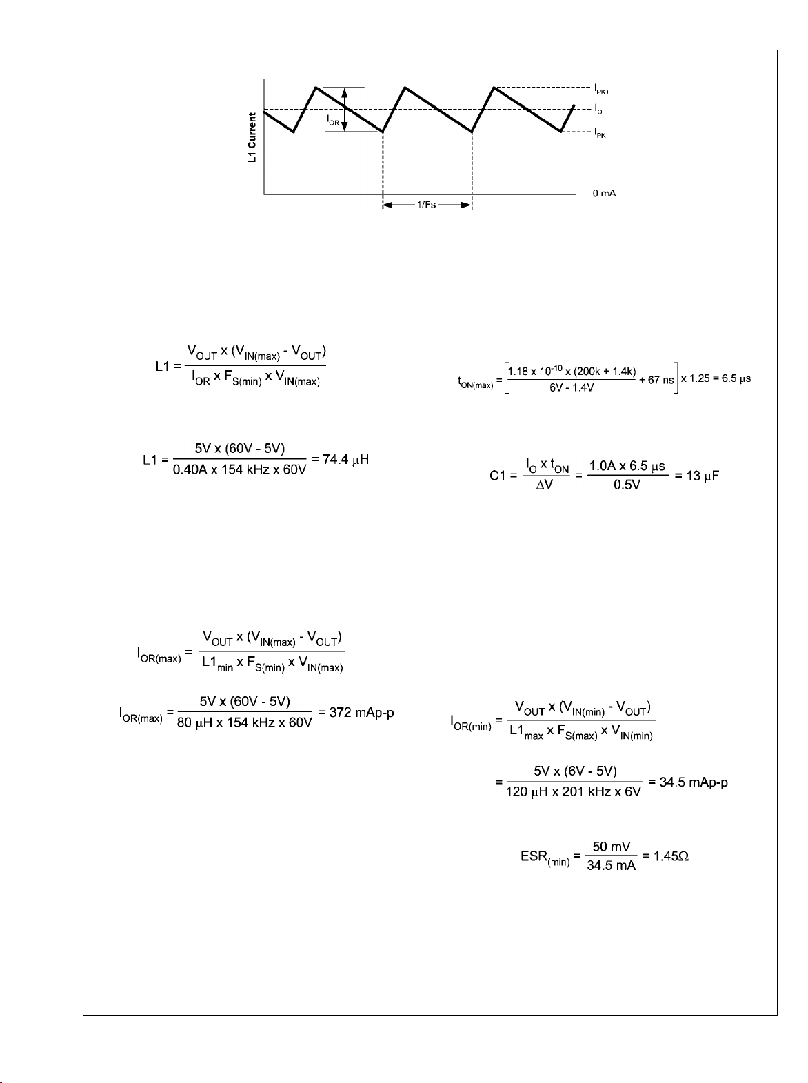
L1: The guideline for choosing the inductor value in this example is that it must keep the circuit’s operation in continuous
conduction mode at minimum load current. This is not a strict
requirement since the LM5010A regulates correctly when in
discontinuous conduction mode, although at a lower frequency. However, to provide an initial value for L1 the above
guideline will be used.
11 www.national.com
LM5010A
20153822
FIGURE 5. Inductor Current
To keep the circuit in continuous conduction mode, the maximum allowed ripple current is twice the minimum load current, or 400 mAp-p. Using this value of ripple current, the
inductor (L1) is calculated using the following:
(11)
where F
- 25%) at V
is the minimum frequency of 154 kHz (205 kHz
S(min)
IN(max)
.
This provides a minimum value for L1 - the next higher standard value (100 µH) will be used. To prevent saturation, and
possible destructive current levels, L1 must be rated for the
peak current which occurs if the current limit and maximum
ripple current are reached simultaneously (IPK in Figure 4).
The maximum ripple amplitude is calculated by re-arranging
Equation 11 using V
value, based on the manufacturer’s tolerance. Assume, for
IN(max)
, F
, and the minimum inductor
S(min)
this exercise, the inductor’s tolerance is ±20%.
(12)
ue (I
), then drops to zero at turn-off. The average current
PK+
into VIN during this on-time is the load current. For a worst
case calculation, C1 must supply this average current during
the maximum on-time. The maximum on-time is calculated at
VIN = 6V using Equation 5, with a 25% tolerance added:
The voltage at VIN should not be allowed to drop below 5.5V
in order to maintain VCC above its UVLO.
Normally a lower value can be used for C1 since the above
calculation is a worst case calculation which assumes the
power source has a high source impedance. A quality ceramic
capacitor with a low ESR should be used for C1.
C2 and R3: Since the LM5010A requires a minimum of 25
mVp-p of ripple at the FB pin for proper operation, the required
ripple at V
is increased by R1 and R2, and is equal to:
OUT
V
= 25 mVp-p x (R1 + R2)/R2 = 50 mVp-p
RIPPLE
This necessary ripple voltage is created by the inductor ripple
current acting on C2’s ESR + R3. First, the minimum ripple
current, which occurs at minimum VIN, maximum inductor
value, and maximum frequency, is determined.
IPK = I
where I
LIM
At the nominal maximum load current of 1.0A, the peak in-
LIM
+ I
= 1.5A + 0.372A = 1.872A
OR(max)
is the maximum guaranteed current limit threshold.
ductor current is 1.186A.
RCL: Since it is obvious that the lower peak of the inductor
current waveform does not exceed 1.0A at maximum load
current (see Figure 5), it is not necessary to increase the current limit threshold. Therefore RCL is not needed for this
exercise. For applications where the lower peak exceeds
1.0A, see the section entitled Increasing The Current Limit
Threshold.
C1: This capacitor limits the ripple voltage at VIN resulting
from the source impedance of the supply feeding this circuit,
and the on/off nature of the switch current into VIN. At maximum load current, when the buck switch turns on, the current
into VIN steps up from zero to the lower peak of the inductor
current waveform (I
www.national.com 12
in Figure 5), ramps up to the peak val-
PK-
(13)
The minimum ESR for C2 is then equal to:
If the capacitor used for C2 does not have sufficient ESR, R3
is added in series as shown in the Block Diagram. The value
chosen for C2 is application dependent, and it is recommended that it be no smaller than 3.3 µF. C2 affects the ripple at
V
, and transient response. Experimentation is usually nec-
OUT
essary to determine the optimum value for C2.
LM5010A
C3: The capacitor at the VCC pin provides noise filtering and
stability, prevents false triggering of the VCC UVLO at the buck
switch on/off transitions, and limits the peak voltage at V
when a high voltage with a short rise time is initially applied
CC
at VIN. C3 should be no smaller than 0.47 µF, and should be
a good quality, low ESR, ceramic capacitor, physically close
to the IC pins.
C4: The recommended value for C4 is 0.022 µF. A high quality
ceramic capacitor with low ESR is recommended as C4 supplies the surge current to charge the buck switch gate at each
turn-on. A low ESR also ensures a complete recharge during
each off-time.
C5: This capacitor suppresses transients and ringing due to
lead inductance at VIN. A low ESR, 0.1 µF ceramic chip capacitor is recommended, located physically close to the
LM5010A.
C6: The capacitor at the SS pin determines the soft-start time,
i.e. the time for the reference voltage at the regulation comparator, and the output voltage, to reach their final value. The
capacitor value is determined from the following:
For a 5 ms softstart time, C6 calculates to 0.022 µF.
D1: A Schottky diode is recommended. Ultra-fast recovery
diodes are not recommended as the high speed transitions at
the SW pin may inadvertently affect the IC’s operation through
external or internal EMI. The diode should be rated for the
maximum VIN (60V), the maximum load current (1A), and the
peak current which occurs when current limit and maximum
ripple current are reached simultaneously (IPK in Figure 4),
previously calculated to be 1.87A. The diode’s forward voltage drop affects efficiency due to the power dissipated during
the off-time. The average power dissipation in D1 is calculated from:
PD1 = VF x IO x (1 - D)
where IO is the load current, and D is the duty cycle.
FINAL CIRCUIT
The final circuit is shown in Figure 6, and its performance is
shown in Figures 7 & 8. Current limit measured approximately
1.3A.
FIGURE 6. Example Circuit
13 www.national.com
20153833

LM5010A
Item Description Value
C1 Ceramic Capacitor (2) 2.2 µF, 100V
C2 Ceramic Capacitor 22 µF, 16V
C3 Ceramic Capacitor 0.47 µF, 16V
C4, C6 Ceramic Capacitor 0.022 µF, 16V
C5 Ceramic Capacitor 0.1 µF, 100V
D1 Schottky Diode 100V, 6A
L1 Inductor 100 µH
R1 Resistor
R2 Resistor
R3 Resistor
R
ON
Resistor
1.0 kΩ
1.0 kΩ
1.5 Ω
200 kΩ
U1 National Semi LM5010A
will either shutdown, or cycle on and off at a low frequency. If
the load current is expected to drop below 500 µA in the application, R1 and R2 should be chosen low enough in value
so they provide the minimum required current at nominal
V
.
OUT
LOW OUTPUT RIPPLE CONFIGURATIONS
For applications where low output voltage ripple is required
the output can be taken directly from the low ESR output capacitor (C2) as shown in Figure 9. However, R3 slightly
degrades the load regulation. The specific component values,
and the application determine if this is suitable.
20153835
FIGURE 7. Efficiency vs Load Current and V
Circuit of Figure 6
FIGURE 8. Frequency vs V
Circuit of Figure 6
IN
IN
20153837
MINIMUM LOAD CURRENT
The LM5010A requires a minimum load current of 500 µA. If
the load current falls below that level, the bootstrap capacitor
(C4) may discharge during the long off-time, and the circuit
20153815
FIGURE 9. Low Ripple Output
Where the circuit of Figure 9 is not suitable, the circuits of
Figure 10 or Figure 11 can be used.
20153848
FIGURE 10. Low Output Ripple Using a Feedforward
Capacitor
In Figure 10, Cff is added across R1 to AC-couple the ripple
at V
directly to the FB pin. This allows the ripple at V
OUT
to be reduced, in some cases considerably, by reducing R3.
In the circuit of Figure 6, the ripple at V
mVp-p at VIN = 6V to 320 mVp-p at VIN = 60V. By adding a
ranged from 50
OUT
OUT
www.national.com 14

LM5010A
1000 pF capacitor at Cff and reducing R3 to 0.75Ω, the
V
ripple was reduced by 50%, ranging from 25 mVp-p to
OUT
160 mVp-p.
20153849
FIGURE 11. Low Output Ripple Using Ripple Injection
To reduce V
used. R3 has been removed, and the output ripple amplitude
ripple further, the circuit of Figure 11 can be
OUT
is determined by C2’s ESR and the inductor ripple current. RA
and CA are chosen to generate a 40-50 mVp-p sawtooth at
their junction, and that voltage is AC-coupled to the FB pin via
CB. In selecting RA and CA, V
ground as the SW pin switches between VIN and -1V. Since
is considered a virtual
OUT
the on-time at SW varies inversely with VIN, the waveform
amplitude at the RA/CA junction is relatively constant. R1 and
R2 must typically be increased to more than 10k each to not
significantly attenuate the signal provided to FB through CB.
Typical values for the additional components are RA = 200k,
CA = 680 pF, and CB = 0.01 µF.
INCREASING THE CURRENT LIMIT THRESHOLD
The current limit threshold is nominally 1.25A, with a minimum
guaranteed value of 1.0A. If, at maximum load current, the
lower peak of the inductor current (I
1.0A, resistor RCL must be added between S
increase the current limit threshold to equal or exceed that
in Figure 5) exceeds
PK-
GND
and I
SEN
to
lower peak current. This resistor diverts some of the recirculating current from the internal sense resistor so that a higher
current level is needed to switch the internal current limit comparator. I
is calculated from:
PK-
(14)
where I
minimum ripple current calculated using Equation 13. RCL is
is the maximum load current, and I
O(max)
OR(min)
is the
calculated from:
(15)
where 0.11Ω is the minimum value of the internal resistance
from SGND to ISEN. The next smaller standard value resistor
should be used for RCL. With the addition of RCL, and when
the circuit is in current limit, the upper peak current out of the
SW pin (IPK in Figure 4) can be as high as:
where I
L1 and diode D1 must be rated for this current. If IPK exceeds
is calculated using Equation 12. The inductor
OR(max)
2A , the inductor value must be increased to reduce the ripple
amplitude. This will necessitate recalculation of I
and RCL.
OR(min)
, I
PK-
Increasing the circuit’s current limit will increase power dissipation and the junction temperature within the LM5010A. See
the next section for guidelines on this issue.
PC BOARD LAYOUT and THERMAL CONSIDERATIONS
The LM5010A regulation, over-voltage, and current limit comparators are very fast, and will respond to short duration noise
pulses. Layout considerations are therefore critical for optimum performance. The layout must be as neat and compact
as possible, and all the components must be as close as possible to their associated pins. The two major current loops
have currents which switch very fast, and so the loops should
be as small as possible to minimize conducted and radiated
EMI. The first loop is that formed by C1, through the VIN to
SW pins, L1, C2, and back to C1. The second loop is that
formed by D1, L1, C2, and the SGND and ISEN pins. The
ground connection from C2 to C1 should be as short and direct as possible, preferably without going through vias. Directly connect the SGND and RTN pin to each other, and they
should be connected as directly as possible to the C1/C2
ground line without going through vias. The power dissipation
within the IC can be approximated by determining the total
conversion loss (PIN - P
losses in the free-wheeling diode and the inductor. The power
), and then subtracting the power
OUT
loss in the diode is approximately:
PD1 = IO x VF x (1-D)
where Io is the load current, VF is the diode’s forward voltage
drop, and D is the duty cycle. The power loss in the inductor
is approximately:
2
PL1 = I
x RL x 1.1
O
where RL is the inductor’s DC resistance, and the 1.1 factor
is an approximation for the AC losses. If it is expected that the
internal dissipation of the LM5010A will produce high junction
temperatures during normal operation, good use of the PC
board’s ground plane can help considerably to dissipate heat.
The exposed pad on the IC package bottom should be soldered to a ground plane, and that plane should both extend
from beneath the IC, and be connected to exposed ground
plane on the board’s other side using as many vias as possible. The exposed pad is internally connected to the IC substrate. The use of wide PC board traces at the pins, where
possible, can help conduct heat away from the IC. The four
No Connect pins on the TSSOP package are not electrically
connected to any part of the IC, and may be connected to
ground plane to help dissipate heat from the package. Judicious positioning of the PC board within the end product,
along with the use of any available air flow (forced or natural
convection) can help reduce the junction temperature.
,
15 www.national.com

Physical Dimensions inches (millimeters) unless otherwise noted
LM5010A
14-Lead TSSOP Package
NS Package Number MXA14A
10-Lead LLP Package
NS Package Number SDC10A
www.national.com 16

Notes
LM5010A
17 www.national.com

Notes
For more National Semiconductor product information and proven design tools, visit the following Web sites at:
Products Design Support
Amplifiers www.national.com/amplifiers WEBENCH www.national.com/webench
Audio www.national.com/audio Analog University www.national.com/AU
Clock Conditioners www.national.com/timing App Notes www.national.com/appnotes
Data Converters www.national.com/adc Distributors www.national.com/contacts
Displays www.national.com/displays Green Compliance www.national.com/quality/green
Ethernet www.national.com/ethernet Packaging www.national.com/packaging
Interface www.national.com/interface Quality and Reliability www.national.com/quality
LVDS www.national.com/lvds Reference Designs www.national.com/refdesigns
Power Management www.national.com/power Feedback www.national.com/feedback
Switching Regulators www.national.com/switchers
LDOs www.national.com/ldo
LED Lighting www.national.com/led
PowerWise www.national.com/powerwise
Serial Digital Interface (SDI) www.national.com/sdi
Temperature Sensors www.national.com/tempsensors
Wireless (PLL/VCO) www.national.com/wireless
THE CONTENTS OF THIS DOCUMENT ARE PROVIDED IN CONNECTION WITH NATIONAL SEMICONDUCTOR CORPORATION
(“NATIONAL”) PRODUCTS. NATIONAL MAKES NO REPRESENTATIONS OR WARRANTIES WITH RESPECT TO THE ACCURACY
OR COMPLETENESS OF THE CONTENTS OF THIS PUBLICATION AND RESERVES THE RIGHT TO MAKE CHANGES TO
SPECIFICATIONS AND PRODUCT DESCRIPTIONS AT ANY TIME WITHOUT NOTICE. NO LICENSE, WHETHER EXPRESS,
IMPLIED, ARISING BY ESTOPPEL OR OTHERWISE, TO ANY INTELLECTUAL PROPERTY RIGHTS IS GRANTED BY THIS
DOCUMENT.
TESTING AND OTHER QUALITY CONTROLS ARE USED TO THE EXTENT NATIONAL DEEMS NECESSARY TO SUPPORT
NATIONAL’S PRODUCT WARRANTY. EXCEPT WHERE MANDATED BY GOVERNMENT REQUIREMENTS, TESTING OF ALL
PARAMETERS OF EACH PRODUCT IS NOT NECESSARILY PERFORMED. NATIONAL ASSUMES NO LIABILITY FOR
APPLICATIONS ASSISTANCE OR BUYER PRODUCT DESIGN. BUYERS ARE RESPONSIBLE FOR THEIR PRODUCTS AND
LM5010A High Voltage 1A Step Down Switching Regulator
APPLICATIONS USING NATIONAL COMPONENTS. PRIOR TO USING OR DISTRIBUTING ANY PRODUCTS THAT INCLUDE
NATIONAL COMPONENTS, BUYERS SHOULD PROVIDE ADEQUATE DESIGN, TESTING AND OPERATING SAFEGUARDS.
EXCEPT AS PROVIDED IN NATIONAL’S TERMS AND CONDITIONS OF SALE FOR SUCH PRODUCTS, NATIONAL ASSUMES NO
LIABILITY WHATSOEVER, AND NATIONAL DISCLAIMS ANY EXPRESS OR IMPLIED WARRANTY RELATING TO THE SALE
AND/OR USE OF NATIONAL PRODUCTS INCLUDING LIABILITY OR WARRANTIES RELATING TO FITNESS FOR A PARTICULAR
PURPOSE, MERCHANTABILITY, OR INFRINGEMENT OF ANY PATENT, COPYRIGHT OR OTHER INTELLECTUAL PROPERTY
RIGHT.
LIFE SUPPORT POLICY
NATIONAL’S PRODUCTS ARE NOT AUTHORIZED FOR USE AS CRITICAL COMPONENTS IN LIFE SUPPORT DEVICES OR
SYSTEMS WITHOUT THE EXPRESS PRIOR WRITTEN APPROVAL OF THE CHIEF EXECUTIVE OFFICER AND GENERAL
COUNSEL OF NATIONAL SEMICONDUCTOR CORPORATION. As used herein:
Life support devices or systems are devices which (a) are intended for surgical implant into the body, or (b) support or sustain life and
whose failure to perform when properly used in accordance with instructions for use provided in the labeling can be reasonably expected
to result in a significant injury to the user. A critical component is any component in a life support device or system whose failure to perform
can be reasonably expected to cause the failure of the life support device or system or to affect its safety or effectiveness.
National Semiconductor and the National Semiconductor logo are registered trademarks of National Semiconductor Corporation. All other
brand or product names may be trademarks or registered trademarks of their respective holders.
Copyright© 2008 National Semiconductor Corporation
For the most current product information visit us at www.national.com
www.national.com
National Semiconductor
Americas Technical
Support Center
Email:
new.feedback@nsc.com
Tel: 1-800-272-9959
National Semiconductor Europe
Technical Support Center
Email: europe.support@nsc.com
German Tel: +49 (0) 180 5010 771
English Tel: +44 (0) 870 850 4288
National Semiconductor Asia
Pacific Technical Support Center
Email: ap.support@nsc.com
National Semiconductor Japan
Technical Support Center
Email: jpn.feedback@nsc.com
 Loading...