

National Semiconductor LM4985 User Manual
LM4985 Evaluation Board
User’s Guide
LM4985 Evaluation Board User’s Guide AN-1452
National Semiconductor
Application Note 1452
Kevin Hoskins
May 2006
Quick Start Guide
Connect the I2C signal generation and interface board to a
computer’s parallel port.
Install LM4985 control software: “LM4985_Software_ver1-
52.”
Amplifier output mode:
For OCL (Output CapacitorLess) mode, place a jumper
across the pins of JP10 and JP11 and across pins 1 and 2 on
JP8.
For C-CUPL (Capacitor Coupled) mode, place a jumper
across pins 2 and 3 on JP8. Leave JP10 and JP11 open.
Apply a 2.3V to 5.0V power supply’s positive voltage output
to the “+” pin on jumpers JP1 and JP2. Apply the power
supply’s ground return to the “-“ on JP1 and JP2.
Connect the supplied 5-wire cable between the I
generation and interface board and the 5-pin connector (JP7
and JP9) on the LM4985 demonstration board.
2
C signal
Apply a stereo audio signal to jumpers JP3 and JP5. Apply
the source’s signal and ground to the “+” pin and the “-“ pin,
respectively.
Connect a load (≥ 16Ω) to JP4 and another load to JP6.
JP4’s “+” pin and JP6’s “+” pin carries the output signals from
the two amplifiers found on pins OUT1 and OUT2, respectively.
Apply power. Make measurements. Plug in a pair of headphones. Enjoy.
Introduction
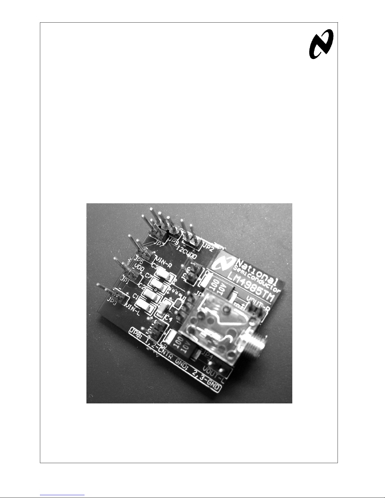
To help the user investigate and evaluate the LM4985’s
performance and capabilities, a fully populated demonstration board is available from the Audio Products Group. This
board is shown in Figure 1. Connected to an external power
supply (2.3V to 5V), a signal source and an I
signal source), the LM4985 demonstration board easily demonstrate the amplifier’s features.
2
C controller (or
© 2006 National Semiconductor Corporation AN201849 www.national.com
20184902
FIGURE 1. The LM4985 Demonstration Board
General Description
The LM4985 is a stereo headphone audio amplifier with an
AN-1452
internal digitally controlled volume control. The LM4985 is
optimized to operate over a power supply voltage range of
2.5V to 5.0V. This amplifier is capable of delivering
40mW
powered by a 3.6V power supply.
Boomer audio power amplifiers were designed specifically to
provide high quality output power with a minimal amount of
external components. To that end, the LM4985 features two
functions that optimize system cost and minimize PCB area:
an integrated, digitally controlled (I
and, for maximum flexibility, an operational mode that eliminates output signal-coupling capacitors (OCL mode). Since
the LM4985 does not require bootstrap capacitors, snubber
networks, or output coupling capacitors, it is optimally suited
for low-power, battery powered potable systems. For added
design flexibility, the LM4985 can also be configured for
single-ended capacitively coupled outputs.
The LM4985 includes an internal input MUX that allows the
signal on either input to appear on either amplifier output and
separate shutdown controls for each stereo channel.
The LM4985 features a shutdown mode for micropower
dissipation, an internal thermal shutdown protection mechanism, and is unity gain stable.
per channel into a 32Ω load at 1% THD when
RMS
2
C bus) volume control
Operating Conditions
Temperature Range –40˚C ≤ TA≤ 85˚C
•
Amplifier Power Supply Voltage 2.3V ≤ VDD≤ 5.0V
•
Board Features
The LM4985 demonstration board has all of the necessary
connections, using 100mil headers, to apply the power supply voltage, the audio input signals, and the I
The amplified audio signal is available on both a stereo
headphone jack and auxiliary output connections. Jumpers
are included to allow the use of either capacitively coupled or
directly coupled amplifier outputs.
Also included with the demonstration board is an I
generation board and software. With this board and the
software, the user can easily control the LM4985’s input
multiplexer, shutdown function, adjustable turn-on time, and
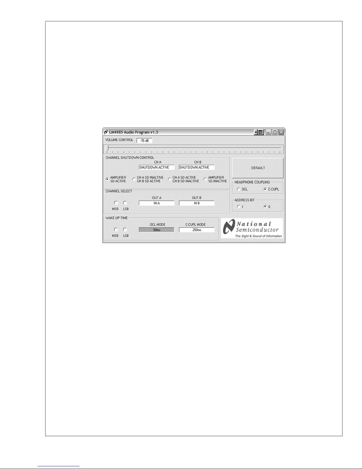
stereo volume control. Figure 3 shows the software’s graphical user interface.
2
C signal inputs.
2
C signal
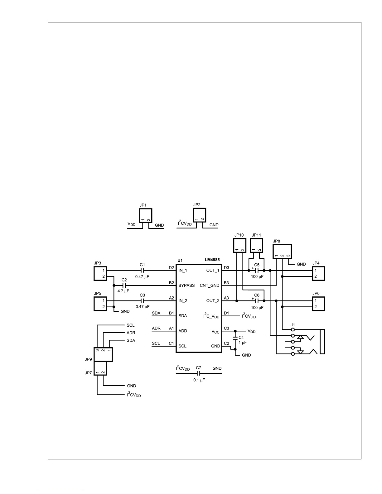
Schematic
Figure 2 shows the LM4985 Demonstration Board schematic. Refer to Table 3 for a list of the connections and their
functions.
www.national.com 2
Figure 2. The LM4985 Demonstration Board Schematic
20184918
Connections
Connecting to the world is accomplished through the 100mil
headers on the LM4985 demonstration board. The functions
of the different headers are detailed in Table 1.
TABLE 1. LM4985 Demonstration Board Connections
Jumper Designation Function or Use
JP1 Power supply connection. Connect an external power supply’s
JP2 If an external I
JP3 This is the connection to the amplifier’s input A (labeled as the
JP4 This is the connection to the amplifier’s output A (labeled as the
JP5 This is the connection to the amplifier’s input B (labeled as the
JP6 This is the connection to the amplifier’s output B (labeled as the
JP7 and JP9 Combined, these jumpers are used for the I
JP8 This three-pin jumper is used when either OCL or C-CUPL modes
JP10 This jumper is used to short the right channel output capacitor C6
JP11 This jumper is used to short the left channel output capacitor C5
positive voltage source to the JP1 pin labeled “+” and the supply’s
ground source to the pin labeled “-.”
2
C power supply voltage is used, connect this
supply’s positive voltage source to the JP2 pin labeled “+” and the
supply’s ground source to the pin labeled “-.” If no external supply
is used, leave this jumper’s pins unconnected.
“left” input on the demonstration board). Apply an external signal
source’s positive voltage to the JP3 pin labeled “+” and the signal
source’s ground reference to the pin labeled “-.”
“left” output on the demonstration board). Connect the JP4 pin
labeled “+” to the positive input of an external signal measurement
device. Connect the JP4 pin labeled “-” to the ground input of an
external signal measurement device. JP4’s pin labeled “+”
corresponds to the headphone jack’s “tip” connection. JP4’s pin
labeled “-“ corresponds to the headphone jack’s “sleeve” (or
ground) connection.
“right” input on the demonstration board). Apply an external signal
source’s positive voltage to the JP5 pin labeled “+” and the signal
source’s ground reference to the pin labeled “-.”
“right” output on the demonstration board). Connect the JP6 pin
labeled “+” to the positive input of an external signal measurement
device. Connect the JP6 pin labeled “-” to the ground input of an
external signal measurement device. JP6’s pin labeled “+”
corresponds to the headphone jack’s “sleeve” connection. JP6’s
pin labeled “-“corresponds to the headphone jack’s “sleeve” (or
ground) connection.
2
C signal inputs.
JP9-pin 1 is for the SDA signal, JP9-pin 2 is for the ADR signal,
2
and JP9-pin 3 is for the SCL signal. JP7-pin 1 is for an I
C VDD
supply voltage supplied by the I2C signal source and JP7-pin 2 is
for ground.
are used. Short pins 1 and 2 together when the OCL mode is
selected. Short pins 2 and 3 together when the C-CUPL mode is
selected.
2
when the OCL mode is selected through the I
C digital interface.
When the LM4985 is used in the C– CUPL mode, leave this jumper
open.
2
when the OCL mode is selected through the I
C digital interface.
When the LM4985 is used in the C– CUPL mode, leave this jumper
open.
AN-1452
www.national.com3
Power Supply Sequencing
The LM4985 uses two power supply voltage: VDDfor the
AN-1452
analog circuitry and I
2
CVDDfor the digital controls (volume,
shutdown, etc.). To ensure proper functionality, apply V
first, followed by I2CVDD. If one power supply is used, V
and I2CVDDcan be connected together. The part will
power-up with shutdown active, the volume control set to
minimum, and the input MUX set so that IN1 and IN2 correspond to OUT1 and OUT2, respectfully (normal stereo).
I2C Signal Generation Board and
Software
The I2C signal generation and interface board, along with the
LM4985 software, will generate the address byte and the
data byte used in the I
2
C signal generation and interface board, please plug it into
I
2
C control data transaction. To use the
a PC’s parallel port (on either a notebook or a desktop
computer).
DD
DD
The software comes with an installer. To install, unzip the file
titled “LM4985_Software_ver1-52.” After the file unzips,
double-click the “setup.exe” file. After it launches, please
follow the installer’s instructions. Setup will create a folder
named “LM4985” in the “Program” folder on the “C” disk (if
the default is used) along with a shortcut of the same name
in the “Programs” folder in the “Start” menu.
Figure 3. The LM4985 Demonstration Board Schematic
The LM4985 program includes controls for the amplifier’s
volume control, shutdown, input MUX, selectable wake-up
time, amplifier output coupling and the I
2
C address bit. The
control program’s on-screen user interface is shown in Figure 3.
The Default button is used to return the LM4985 to its
power-on reset state (minimum volume setting, shutdown on
both amplifiers active, standard stereo mode, capacitively
coupled output, and minimum wake-up time.
The LM4985’s stereo VOLUME CONTROL has 32 steps
and a gain range of –76dB to 18dB. It is controlled using the
slider located at the top of the program’s window. Each time
the slider is moved from one tick mark to another, the program updates the amplifier’s volume control.
The CHANNEL SHUTDOWN CONTROL has four radio buttons. From left to right, the first button controls the shutdown
function of both amplifiers. When selected, both amplifiers
are placed in shutdown mode. The middle pair of buttons
places a single amplifier channel in shutdown mode. The
first of the pair deactivates channel A’s shutdown and activates channel B’s shutdown. The second in the pair activates channel A’s shutdown and deactivates channel B’s
shutdown. The last shutdown button deactivates both channels’ shutdown, allowing full, two-channel amplifier operation.
20184927
There is a protocol that one must follow when placing an
individual amplifier channel in shutdown while the other
channel remains active. The protocol requires activating
both channel’s shutdown simultaneously, then deactivating
the shutdown of the channel whose output is desired (or
leaving the desired channel in shutdown mode). This protocol is required whether using this software or a user-created
routine. Further, when operating in the C-CUPL mode, a
short delay time is required before activating one channel
after placing both channels in shutdown. If the user finds that
both channels activate when only one was chosen, increase
the delay.
The next section, CHANNEL SELECT, is used to choose
which input signal is internally routed to which amplifier
channel. The power-on or reset state is standard stereo: the
signal applied to input IN A is routed to the OUT A amplifier
and the signal applied to input IN B is routed to the OUT B
amplifier. The other three modes are the signal applied to IN
A is routed to both channels, the signal applied to IN B is
routed to both channels, and reverse stereo (the signal
applied to IN A is routed to amplifier B and the signal applied
to IN B is routed to amplifier A).
www.national.com 4
 Loading...