

National Semiconductor LM49250 User Manual
LM49250 Evaluation Board
User Guide
National Semiconductor
Application Note 1680
Nisha Patel
March 9, 2010
Introduction
The LM49250 is a fully integrated audio subsystem designed
for stereo cell phone applications. The LM49250 combines
2.5W stereo Class D speaker drivers with stereo ground referenced headphone drivers, a class AB earpiece driver, National 3D enhancement, volume control and input mixer into
a single device. The filterless class D amplifiers deliver
1.19W/channel into an 8Ω load with <1% THD+N from a 5V
supply.
The LM49250 features a new circuit technology that utilizes
a charge pump to generate a negative supply voltage. This
allows the outputs to be biased about ground, thereby eliminating output-coupling capacitors typically used with normal
single-ended loads. To supply the required voltage level to
the ground referenced amplifier, an LDO has been integrated.
For improved noise immunity, the LM49250 features fully differential left, right and mono inputs. The three inputs can be
mixed/multiplexed to either the loudspeaker, headphone or
earpiece amplifiers. The left and right differential inputs can
be used as separate single-ended inputs, mixing multiple
stereo audio sources. The mixer, volume control, and device
mode select are controlled through an I2C compatible interface.
Output short circuit and thermal overload protection prevent
the device from being damaged during fault conditions. Superior click and pop suppression eliminates audible transients
on power-up/down and during shutdown.
The LM49250 Evaluation board (shown in Figure 1) allows
the user to easily evaluate the performance and characteristics of the LM49250 device. It provides connectors for audio
inputs, audio outputs, I2C control, power supply, and shutdown control.
Quick Start
1. Connect a shunt across the center pin (I2C VDD) and VDD
pin of J9 (I2CVDD = VDD).
2. Connect a shunt across the center RESET pin and the “+”
terminal of J4 (I2C reset pin).
3. Connect a 4Ω or 8Ω speaker across the “+” and “-” pins of
J2 (left loudspeaker output) and J3 (right loudspeaker
output).
4. Connect stereo headphones to the headphone jack (U2).
5. Connect a 16Ω or 32Ω speaker across the “+” and “-” pins
of J1 (earpiece output).
6. Connect a 3.6V power supply to the VDD pin of J8, and the
power supply ground source to the GND pin of J8.
7. Apply a positive audio signal source to the “+” terminals of
J5 (right input), J6 (left input), and J7 (mono input), and a
negative audio signal source to the “-” terminals of J5 (right
input), J6 (left input), and J7 (mono input).
8. Connect the USB interface card to a PC with the USB cable.
Connect cable attached to USB interface card to the
I2C interface jumper (J10)on demo board.
9. Open LM49250 I2C interface software.
10. Turn on power supply and audio source.
11. In the LM49250 I2C interface software (see Figure 2)
select:
a. “ON” for Earpiece, Left Loudspeaker, Right Loudspeaker,
Left Headphone, and Right Headphone
b. Mode “2” for Loudspeaker Output Mode, Headphone
Output Mode, and Earpiece Output Mode
12. Select Chip Power to “ON” to enable the device.
13. Adjust the Left, Right, and Mono Volume Control to obtain
the desired output level.
Operating Conditions
• Temperature Range
–40°C ≤ TA ≤ +85°C
• Supply Voltage
(VDD = V
DD(LS)
= V
DD(CP)
)
2.7V ≤ VDD ≤ 5.5V
• I2C Supply Voltage
1.7V ≤ I2CVDD ≤ 5.5V
I2CVDD ≤ V
DD
© 2010 National Semiconductor Corporation 300291 www.national.com
LM49250 Evaluation Board User Guide AN-1680
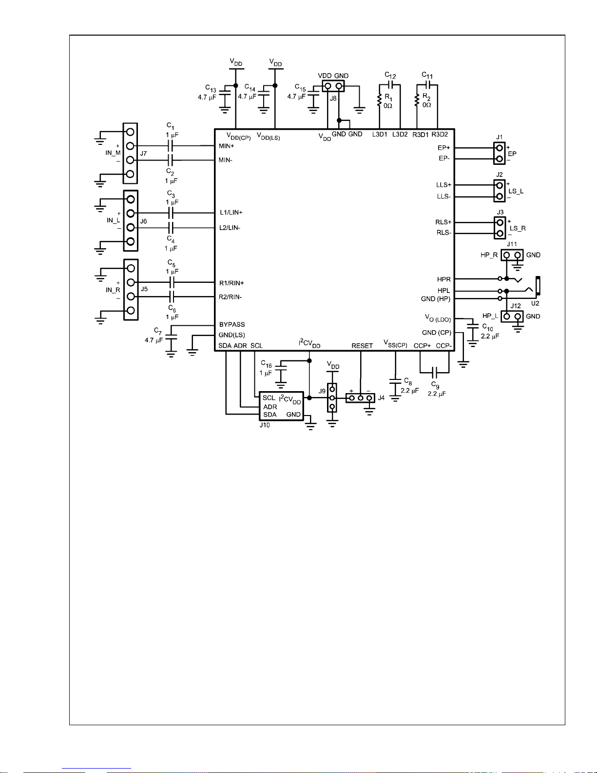
30029105
FIGURE 1. Evaluation Board Schematic
www.national.com 2
AN-1680
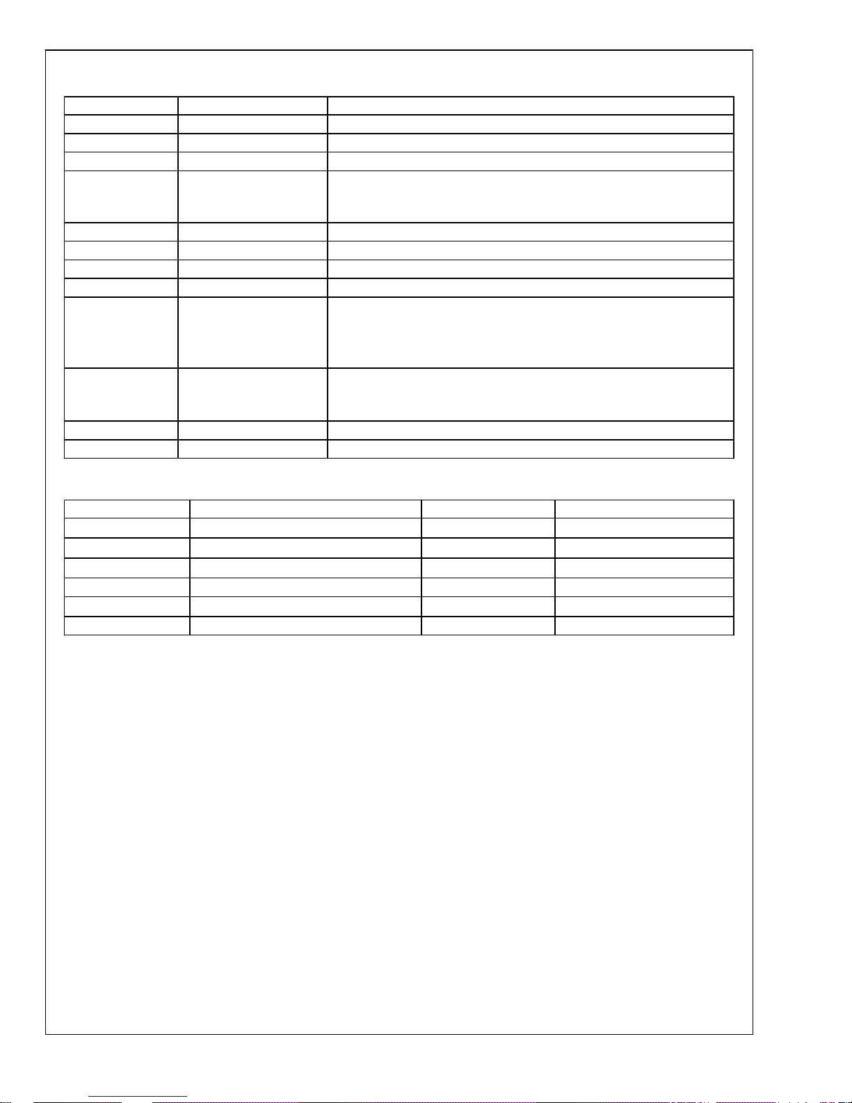
TABLE 1. Board Connectors
Designator Label Function
J1 EP Mono BTL earpiece audio output
J2 LS_L Left loudspeaker class D audio output
J3 LS_R Right loudspeaker class D audio output
J4 RESET I2C Reset Pin - For normal operation short the center RESET pin to the “+”
pin. To reset the PWR_ON bit in the shutdown control register short the center
RESET pin to the “-” terminal.
J5 IN_R Right, single ended or differential, audio input terminal
J6 IN_L Left, single ended or differential, audio input terminal
J7 IN_M Mono differential audio input terminal
J8 VDD GND Power Supply Connection
J9
I2CV
DD
If a separate I2C power supply voltage is used: Connect the positive voltage
source to the center I2CVDD terminal and the ground source to the pin on J9
labeled GND. If a separate I2C power supply is not used: Connect the center
I2CVDD to the pin on J9 labeled VDD.
J10
I2C signal terminals. Pin 1 is for the SCL signal, pin 2 is for the ADR signal,
pin 3 is for the SDA signal, pin 4 is for I2C VDD, and pin 5 is ground (as labeled
on the evaluation board).
J11 HP_R Right ground referenced headphone output terminal
J12 HP_L Left ground referenced headphone output terminal
TABLE 2. Evaluation Board Bill of Materials
Designator Part Description Manufacturer Part Number
C1 – C6
ceramic capacitor 1μF 16V X7R 1206 10%
muRata GRM319R71C105KC11D
C7, C13, C14, C15
ceramic capacitor 2.2μF 16V X5R 0805
muRata GRM21BR61C225KA88L
C8, C9, C10
ceramic capacitor 2.2μF 16V X5R 0805
muRata GRM21BR61C225KA88L
C11, C12 ceramic capacitor 68nF 16V X7R 0805 muRata GRM188R71C683KA01D
C16
ceramic capacitor 1μF 16V X7R 0805
muRata GRM21BR71C105KA01L
R1, R2 resistor 0W 1/8W 5% 0805 SMD
3 www.national.com
AN-1680
 Loading...