

May 30, 2008
LM4030
SOT-23 Ultra-High Precision Shunt Voltage Reference
LM4030 SOT-23 Ultra-High Precision Shunt Voltage Reference
General Description
The LM4030 is an ultra-high precision shunt voltage reference, having exceptionally high initial accuracy (0.05%) and
temperature stability (10ppm/°C). The LM4030 is available
with fixed voltage options of 2.5V and 4.096V. Despite the tiny
SOT23 package, the LM4030 exhibits excellent thermal hysteresis (75ppm) and long-term stability (40ppm) as well as
immunity to board stress effects.
The LM4030 is designed to operate without an external capacitor, but any capacitor up to 10µF may be used. The
LM4030 can be powered off as little as 120µA (max) but is
capable of shunting up to 30mA continuously. As with any
shunt reference, the LM4030 can be powered off of virtually
any supply and is a simple way to generate a highly accurate
system reference.
The LM4030 is available in three grades (A, B, and C). The
best grade devices (A) have an initial accuracy of 0.05% with
guaranteed temperature coefficient of 10 ppm/°C or less,
while the lowest grade parts (C) have an initial accuracy of
0.15% and a temperature coefficient of 30 ppm/°C.
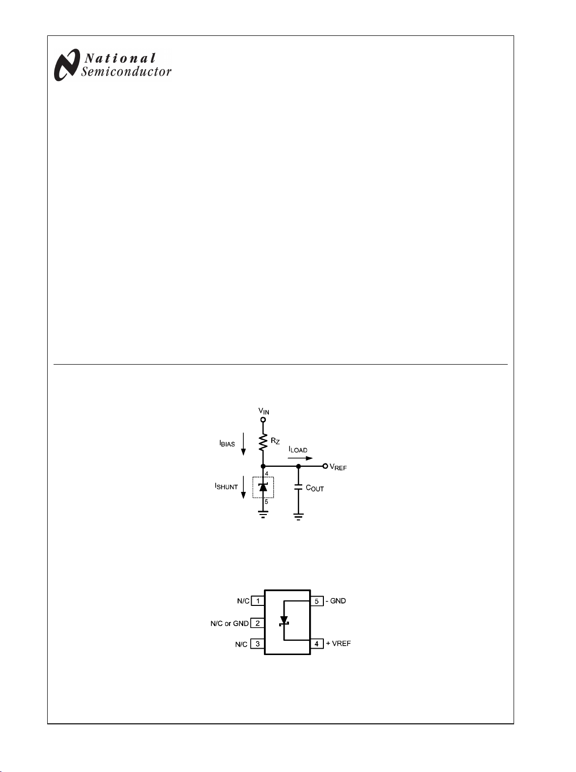
Typical Application Circuit
Features
High output voltage accuracy 0.05%
■
Low temperature coefficient 10 ppm/°C
■
Extended temperature operation -40-125°C
■
Excellent thermal hysteresis, 75ppm
■
Excellent long-term stability, 40ppm
■
High immunity to board stress effects
■
Capable of handling 50 mA transients
■
Voltage options 2.5V, 4.096V
■
SOT23-5 Package
■
Applications
Data Acquisition/Signal path
■
Test and Measurement
■
Automotive & Industrial
■
Communications
■
Instrumentation
■
Power Management
■
30046301
Connection Diagram
Top View
SOT23-5 Package
NS Package Number MF05A
© 2008 National Semiconductor Corporation 300463 www.national.com
30046302

Ordering Information
LM4030
Input Output Voltage Accuracy at
25°C And Temperature Coefficient
0.05%, 10 ppm/°C max (A grade) LM4030AMF-2.5 LM4030AMFX-2.5 R5JA
0.10%, 20 ppm/°C max (B grade) LM4030BMF-2.5 LM4030BMFX-2.5 R5JB
0.15%, 30 ppm/°C max (C grade) LM4030CMF-2.5 LM4030CMFX-2.5 R5JC
Pin Descriptions
Pin # Name Function
1 N/C No connect pin, leave floating
2 GND, N/C Ground or no connect
3 N/C No connect pin, leave floating
4 VREF Reference voltsge
5 GND Ground
LM4030 Supplied as 1000
units, Tape and Reel
LM4030AMF-4.096 LM4030AMFX4.096 R5KA
LM4030BMF-4.096 LM4030BMFX4.096 R5KB
LM4030CMF-4.096 LM4030CMFX4.096 R5KC
LM4030 Supplied as 3000 units,
Tape and Reel
Part Marking
www.national.com 2

LM4030
Absolute Maximum Ratings (Note 1)
If Military/Aerospace specified devices are required,
please contact the National Semiconductor Sales Office/
Distributors for availability and specifications.
Maximum Voltage on any input -0.3 to 6V
Power Dissipation (TA = 25°C)
(Note 2) 350mW
Storage Temperature Range −65°C to 150°C
Lead Temperature (soldering, 10sec) 260°C
Infrared (15sec) 220°C
ESD Susceptibility (Note 3)
Human Body Model 2kV
Operating Ratings
Maximum Continuous Shunt Current 30mA
Maximum Shunt Current (<1s) 50mA
Junction Temperature Range (TJ) −40°C to
+125°C
Vapor Phase (60 sec) 215°C
Electrical Characteristics
LM4030-2.5 (V
the junction temperature (TJ) range of -40°C to +125°C. Minimum and Maximum limits are guaranteed through test, design, or
statistical correlation. Typical values represent the most likely parametric norm at TJ = 25°C, and are provided for reference
purposes only.
Symbol Parameter Conditions Min
V
REF
Reverse Breakdown Voltage Tolerance (I
LM4030A-2.5 (A Grade - 0.05%) -0.05 0.05 %
LM4030B-2.5 (B Grade - 0.10%) -0.10 0.10 %
LM4030C-2.5 (C Grade - 0.15%) -0.15 0.15 %
I
RMIN
TC Temperature Coefficient (Note 6)
LM4030A-2.5
LM4030B-2.5
LM4030C-2.5
ΔV
/ΔI
REF
SHUNT
ΔV
REF
V
HYST
V
N
Reverse Breakdown Voltage I
Minimum Operating Current 120 µA
Reverse Breakdown Voltage Change
with Current
Long Term Stability (Note 7) 1000 Hrs, TA = 30°C 40 ppm
Thermal Hysteresis (Note 8)
Output Noise Voltage (Note 9) 0.1 Hz to 10 Hz 105 µV
= 2.5V) Limits in standard type are for T
OUT
= 120µA 2.5 V
SHUNT
SHUNT
0°C ≤ TJ ≤ + 85°C
-40°C ≤ TJ ≤ +125°C
-40°C ≤ TJ ≤ +125°C
-40°C ≤ TJ ≤ +125°C
160µA ≤ I
-40°C ≤ TJ ≤ +125°C
= 120µA)
≤ 30mA
SHUNT
= 25°C only, and limits in boldface type apply over
J
Typ
(Note 4)
(Note 5)
10
20
20
30
Max
(Note 4)
Unit
ppm / °C
ppm / °C
ppm / °C
ppm / °C
25 110 ppm / mA
75 ppm
PP
3 www.national.com

Electrical Characteristics
LM4030-4.096 (V
LM4030
over the junction temperature (TJ) range of -40°C to +125°C. Minimum and Maximum limits are guaranteed through test, design,
or statistical correlation. Typical values represent the most likely parametric norm at TJ = 25°C, and are provided for reference
purposes only.
Symbol Parameter Conditions Min
V
REF
Reverse Breakdown Voltage I
Reverse Breakdown Voltage Tolerance ( I
LM4030A-4.096 (A Grade - 0.05%) -0.05 0.05 %
LM4030B-4.096 (B Grade - 0.10%) -0.10 0.10 %
LM4030C-4.096 (C Grade - 0.15%) -0.15 0.15 %
I
RMIN
Minimum Operating Current 130 µA
TC Temperature Coefficient (Note 6)
LM4030A-4.096
LM4030B-4.096
LM4030C-4.096
ΔV
REF
/ΔI
Reverse Breakdown Voltage
LOAD
Change with Current
ΔV
V
REF
HYST
V
N
Long Term Stability (Note 7) 1000 Hrs, TA = 30°C 40 ppm
Thermal Hysteresis (Note 8)
Output Noise Voltage (Note 9) 0.1 Hz to 10 Hz 165 µV
= 4.096V) Limits in standard type are for T
OUT
= 130µA 4.096 V
SHUNT
= 130µA)
SHUNT
0°C ≤ TJ ≤ + 85°C
-40°C ≤ TJ ≤ +125°C
-40°C ≤ TJ ≤ +125°C
-40°C ≤ TJ ≤ +125°C
160µA ≤ I
SHUNT
-40°C ≤ TJ ≤ +125°C
≤ 30mA
= 25°C only, and limits in boldface type apply
J
(Note
4)
Typ
(Note
5)
Max
(Note 4)
10
20
20
30
15 95 ppm / mA
75 ppm
Unit
ppm / °C
ppm / °C
ppm / °C
ppm / °C
PP
Note 1: Absolute Maximum Ratings indicate limits beyond which damage may occur to the device. Operating Ratings indicate conditions for which the device is
intended to be functional, but do not guarantee specific performance limits. For guaranteed specifications, see Electrical Characteristics.
Note 2: Without PCB copper enhancements. The maximum power dissipation must be de-rated at elevated temperatures and is limited by T
junction temperature), θ
P
= (T
DissMAX
Note 3: The human body model is a 100 pF capacitor discharged through a 1.5 kΩ resistor into each pin.
Note 4: Limits are 100% production tested at 25°C. Limits over the operating temperature range are guaranteed through correlation using Statistical Quality
Control.
Note 5: Typical numbers are at 25°C and represent the most likely parametric norm.
Note 6: Temperature coefficient is measured by the "Box" method; i.e., the maximum ΔV
Note 7: Long term stability is V
Note 8: Thermal hysteresis is defined as the change in +25°C output voltage before and after cycling the device from (-40°C to 125°C) eight times.
Note 9: Low frequency peak-to-peak noise measured using first-order 0.1 Hz HPF and second-order 10 Hz LPF.
JMAX
(junction to ambient thermal resistance) and TA (ambient temperature). The maximum power dissipation at any temperature is:
J-A
- TA) /θ
up to the value listed in the Absolute Maximum Ratings. θ
J-A
@25°C measured during 1000 hrs. This measurement is taken for IR = 500 µA.
REF
for SOT23-5 package is 220°C/W, T
J-A
is divided by the maximum ΔT.
REF
JMAX
= 125°C.
JMAX
(maximum
www.national.com 4

Typical Performance Characteristics for 2.5V
LM4030
Output Voltage vs Temperature
Start Up - 120 µA
0.1 - 10 Hz Peak-to-Peak Noise
30046303
30046332
Start Up - 50 mA
30046304
Reverse Breakdown Voltage Change with Current
30046314
30046305
Reverse Dynamic Impedance vs Frequency
30046340
5 www.national.com

Typical Performance Characteristics for 4.096V
LM4030
Output Voltage vs Temperature
30046349
0.1 - 10 Hz Peak-to-Peak Noise
30046306
Start Up - 130 µA
30046307
Reverse Breakdown Voltage Change with Current
Start Up - 50 mA
30046308
Reverse Dynamic Impedance vs Frequency
30046312
www.national.com 6
30046341

Typical Performance Characteristics
LM4030
Forward Characteristic
Minimum Operating Current
Load Transient Response
30046313
30046311
Noise Spectrum
Thermal Hysteresis Distribution
30046316
30046330
30046317
Output Voltage vs Thermal Cycle (-40°C to 125°C)
30046351
7 www.national.com

LM4030
Long Term Stability (TA = 25°C)
Long Term Stability (TA =125°C)
30046347
30046348
www.national.com 8

LM4030
Application Information
THEORY OF OPERATION
The LM4030 is an ultra-high precision shunt voltage reference, having exceptionally high initial accuracy (0.05%) and
temperature stability (10ppm/°C). The LM4030 is available
with fixed voltage options of 2.5V and 4.096V. Despite the tiny
SOT23 package, the LM4030 exhibits excellent thermal hysteresis (75ppm) and long-term stability (25ppm). The LM4030
is designed to operate without an external capacitor, but any
capacitor up to 10 µF may be used. The LM4030 can be powered off as little as 120 µA (max) but is capable of shunting
up to 30 mA continuously. The typical application circuit for
the LM4030 is shown in Figure 1.
30046301
FIGURE 1. Typical Application Circuit
COMPONENT SELECTION
A resistor must be chosen to set the maximum operating current for the LM4030 (RZ in Figure 1). The value of the resistor
can be calculated using the following equation:
RZ = (VIN - V
RZ is chosen such that the total current flowing through RZ is
greater than the maximum load current plus the minimum operating current of the reference itself. This ensures that the
reference is never starved for current. Running the LM4030
at higher currents is advantageous for reducing noise. The
reverse dynamic impedance of the V
ly with the shunted current (see Figure 2) leading to higher
rejection of noise emanating from the input supply and from
EMI (electro-magnetic interferrence).
REF
)/(I
MIN_OPERATING
REF
+ I
LOAD_MAX
)
node scales inverse-
The LM4030 is designed to operate with or without a bypass
capacitor (C
up to 10 μF. The use of a bypass capacitor can improve tran-
in Figure 1) and is stable with capacitors of
OUT
sient response and reduce broadband noise. Additionally, a
bypass capacitor will counter the rising reverse dynamic
impedance at higher frequencies improving noise immunity
(see Figure 3).
30046345
FIGURE 3. Reverse Dynamic Impedance vs C
OUT
As with other regulators, an external capacitor reduces the
amplitude of the V
loading takes place. The capacitor should be placed as close
transient when a sudden change in
REF
to the part as possible to reduce the effects of unwanted board
parasitics.
THERMAL HYSTERESIS
Thermal hysteresis is the defined as the change in output
voltage at 25°C after some deviation from 25°C. This is to say
that thermal hysteresis is the difference in output voltage between two points in a given temperature profile. An illustrative
temperature profile is shown in Figure 4.
30046346
FIGURE 2. Reverse Dynamic Impedance vs I
OUT
30046318
FIGURE 4. Illustrative Temperature Profile
This may be expressed analytically as the following:
Where
V
= Thermal hysteresis expressed in ppm
HYS
V
= Nominal preset output voltage
REF
V
= V
REF1
9 www.national.com
before temperature fluctuation
REF

V
= V
REF2
after temperature fluctuation.
REF
The LM4030 features a low thermal hysteresis of 75 ppm
LM4030
(typical) from -40°C to 125°C after 8 temperature cycles.
TEMPERATURE COEFFICIENT
Temperature drift is defined as the maximum deviation in output voltage over the temperature range. This deviation over
temperature may be illustrated as shown in Figure 5.
shifts in VREF arise due to offsets between matched devices
within the regulation loop. Both passive and active devices
naturally experience drift over time and stress and temperature gradients across the silicon die also generate offset. The
LM4030 incorporates a dynamic offset cancellation scheme
which compensates for offsets developing within the regulation loop. This gives the LM4030 excellent long-term stability
(40 ppm typical) and thermal hysteresis performance (75ppm
typical), as well as substantial immunity to PCB stress effects,
despite being packaged in a tiny SOT23.
EXPRESSION OF ELECTRICAL CHARACTERISTICS
Electrical characteristics are typically expressed in mV, ppm,
or a percentage of the nominal value. Depending on the application, one expression may be more useful than the other.
To convert one quantity to the other one may apply the following:
ppm to mV error in output voltage:
30046320
FIGURE 5. Illustrative V
vs Temperature Profile
REF
Temperature coefficient may be expressed analytically as the
following:
TD = Temperature drift
V
= Nominal preset output voltage
REF
V
temperature range
V
temperature range
= Minimum output voltage over operating
REF_MIN
= Maximum output voltage over operating
REF_MAX
ΔT = Operating temperature range.
The LM4030 features a low temperature drift of 10ppm (max)
to 30ppm (max), depending on the grade.
DYNAMIC OFFSET CANCELLATION AND LONG TERM STABILITY
Aside from initial accuracy and drift performance, other specifications such as thermal hysteresis and long-term stability
can affect the accuracy of a voltage reference, especially over
the lifetime of the application. The reference voltage can also
shift due to board stress once the part is mounted onto the
PCB and during subsequent thermal cycles. Generally, these
Where:
V
is in volts (V) and V
REF
is in milli-volts (mV).
ERROR
Bit error (1 bit) to voltage error (mV):
V
is in volts (V), V
REF
number of bits.
is in milli-volts (mV), and n is the
ERROR
mV to ppm error in output voltage:
Where:
V
is in volts (V) and V
REF
is in milli-volts (mV).
ERROR
Voltage error (mV) to percentage error (percent):
Where:
V
is in volts (V) and V
REF
is in milli-volts (mV).
ERROR
www.national.com 10

LM4030
PRINTED CIRCUIT BOARD and LAYOUT CONSIDERATIONS
The LM4030 has a very small change in reverse voltage with
current (25ppm/mA typical) so large variations in load current
(up to 50mA) should not appreciably shift VREF. Parasitic resistance between the LM4030 and the load introduces a
voltage drop proportional to load current and should be minimized. The LM4030 should be placed as close to the load it
is driving as the layout will allow. The location of RZ is not
important, but C
possible so added ESR does not degrade the transient per-
should be as close to the LM4030 as
OUT
formance.
11 www.national.com

Physical Dimensions inches (millimeters) unless otherwise noted
LM4030
SOT23-5 Package
NS Package Number MF05A
www.national.com 12

Notes
LM4030
13 www.national.com

Notes
For more National Semiconductor product information and proven design tools, visit the following Web sites at:
Products Design Support
Amplifiers www.national.com/amplifiers WEBENCH www.national.com/webench
Audio www.national.com/audio Analog University www.national.com/AU
Clock Conditioners www.national.com/timing App Notes www.national.com/appnotes
Data Converters www.national.com/adc Distributors www.national.com/contacts
Displays www.national.com/displays Green Compliance www.national.com/quality/green
Ethernet www.national.com/ethernet Packaging www.national.com/packaging
Interface www.national.com/interface Quality and Reliability www.national.com/quality
LVDS www.national.com/lvds Reference Designs www.national.com/refdesigns
Power Management www.national.com/power Feedback www.national.com/feedback
Switching Regulators www.national.com/switchers
LDOs www.national.com/ldo
LED Lighting www.national.com/led
PowerWise www.national.com/powerwise
Serial Digital Interface (SDI) www.national.com/sdi
Temperature Sensors www.national.com/tempsensors
Wireless (PLL/VCO) www.national.com/wireless
THE CONTENTS OF THIS DOCUMENT ARE PROVIDED IN CONNECTION WITH NATIONAL SEMICONDUCTOR CORPORATION
(“NATIONAL”) PRODUCTS. NATIONAL MAKES NO REPRESENTATIONS OR WARRANTIES WITH RESPECT TO THE ACCURACY
OR COMPLETENESS OF THE CONTENTS OF THIS PUBLICATION AND RESERVES THE RIGHT TO MAKE CHANGES TO
SPECIFICATIONS AND PRODUCT DESCRIPTIONS AT ANY TIME WITHOUT NOTICE. NO LICENSE, WHETHER EXPRESS,
IMPLIED, ARISING BY ESTOPPEL OR OTHERWISE, TO ANY INTELLECTUAL PROPERTY RIGHTS IS GRANTED BY THIS
DOCUMENT.
TESTING AND OTHER QUALITY CONTROLS ARE USED TO THE EXTENT NATIONAL DEEMS NECESSARY TO SUPPORT
NATIONAL’S PRODUCT WARRANTY. EXCEPT WHERE MANDATED BY GOVERNMENT REQUIREMENTS, TESTING OF ALL
PARAMETERS OF EACH PRODUCT IS NOT NECESSARILY PERFORMED. NATIONAL ASSUMES NO LIABILITY FOR
APPLICATIONS ASSISTANCE OR BUYER PRODUCT DESIGN. BUYERS ARE RESPONSIBLE FOR THEIR PRODUCTS AND
APPLICATIONS USING NATIONAL COMPONENTS. PRIOR TO USING OR DISTRIBUTING ANY PRODUCTS THAT INCLUDE
NATIONAL COMPONENTS, BUYERS SHOULD PROVIDE ADEQUATE DESIGN, TESTING AND OPERATING SAFEGUARDS.
LM4030 SOT-23 Ultra-High Precision Shunt Voltage Reference
EXCEPT AS PROVIDED IN NATIONAL’S TERMS AND CONDITIONS OF SALE FOR SUCH PRODUCTS, NATIONAL ASSUMES NO
LIABILITY WHATSOEVER, AND NATIONAL DISCLAIMS ANY EXPRESS OR IMPLIED WARRANTY RELATING TO THE SALE
AND/OR USE OF NATIONAL PRODUCTS INCLUDING LIABILITY OR WARRANTIES RELATING TO FITNESS FOR A PARTICULAR
PURPOSE, MERCHANTABILITY, OR INFRINGEMENT OF ANY PATENT, COPYRIGHT OR OTHER INTELLECTUAL PROPERTY
RIGHT.
LIFE SUPPORT POLICY
NATIONAL’S PRODUCTS ARE NOT AUTHORIZED FOR USE AS CRITICAL COMPONENTS IN LIFE SUPPORT DEVICES OR
SYSTEMS WITHOUT THE EXPRESS PRIOR WRITTEN APPROVAL OF THE CHIEF EXECUTIVE OFFICER AND GENERAL
COUNSEL OF NATIONAL SEMICONDUCTOR CORPORATION. As used herein:
Life support devices or systems are devices which (a) are intended for surgical implant into the body, or (b) support or sustain life and
whose failure to perform when properly used in accordance with instructions for use provided in the labeling can be reasonably expected
to result in a significant injury to the user. A critical component is any component in a life support device or system whose failure to perform
can be reasonably expected to cause the failure of the life support device or system or to affect its safety or effectiveness.
National Semiconductor and the National Semiconductor logo are registered trademarks of National Semiconductor Corporation. All other
brand or product names may be trademarks or registered trademarks of their respective holders.
Copyright© 2008 National Semiconductor Corporation
For the most current product information visit us at www.national.com
www.national.com
National Semiconductor
Americas Technical
Support Center
Email: support@nsc.com
Tel: 1-800-272-9959
National Semiconductor Europe
Technical Support Center
Email: europe.support@nsc.com
German Tel: +49 (0) 180 5010 771
English Tel: +44 (0) 870 850 4288
National Semiconductor Asia
Pacific Technical Support Center
Email: ap.support@nsc.com
National Semiconductor Japan
Technical Support Center
Email: jpn.feedback@nsc.com
 Loading...