

LM2734
Thin SOT23 1A Load Step-Down DC-DC Regulator
LM2734 Thin SOT23 1A Load Step-Down DC-DC Regulator
June 4, 2008
General Description
The LM2734 regulator is a monolithic, high frequency, PWM
step-down DC/DC converter in a 6-pin Thin SOT23 package.
It provides all the active functions to provide local DC/DC
conversion with fast transient response and accurate regulation in the smallest possible PCB area.
With a minimum of external components and online design
support through WEBENCH®™, the LM2734 is easy to use.
The ability to drive 1A loads with an internal 300mΩ NMOS
switch using state-of-the-art 0.5µm BiCMOS technology results in the best power density available. The world class
control circuitry allows for on-times as low as 13ns, thus supporting exceptionally high frequency conversion over the entire 3V to 20V input operating range down to the minimum
output voltage of 0.8V. Switching frequency is internally set
to 550kHz (LM2734Y) or 1.6MHz (LM2734X), allowing the
use of extremely small surface mount inductors and chip capacitors. Even though the operating frequencies are very
high, efficiencies up to 90% are easy to achieve. External
shutdown is included, featuring an ultra-low stand-by current
of 30nA. The LM2734 utilizes current-mode control and internal compensation to provide high-performance regulation
over a wide range of operating conditions. Additional features
include internal soft-start circuitry to reduce inrush current,
pulse-by-pulse current limit, thermal shutdown, and output
over-voltage protection.
Features
Thin SOT23-6 package
■
3.0V to 20V input voltage range
■
0.8V to 18V output voltage range
■
1A output current
■
550kHz (LM2734Y) and 1.6MHz (LM2734X)
■
switching frequencies
300mΩ NMOS switch
■
30nA shutdown current
■
0.8V, 2% internal voltage reference
■
Internal soft-start
■
Current-Mode, PWM operation
■
WEBENCH® online design tool
■
Thermal shutdown
■
LM2734XQ/LM2734YQ are AEC-Q100 Grade 1 qualified
■
and are manufactured on an Automotive Grade Flow
Applications
Local Point of Load Regulation
■
Core Power in HDDs
■
Set-Top Boxes
■
Battery Powered Devices
■
USB Powered Devices
■
DSL Modems
■
Notebook Computers
■
Automotive
■
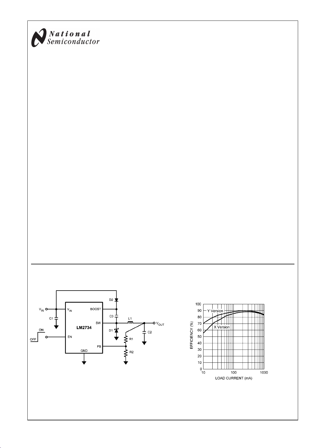
Typical Application Circuit
Efficiency vs Load Current
VIN = 5V, V
20102301
WEBENCH™ is a trademark of Transim.
© 2008 National Semiconductor Corporation 201023 www.national.com
OUT
= 3.3V
20102345
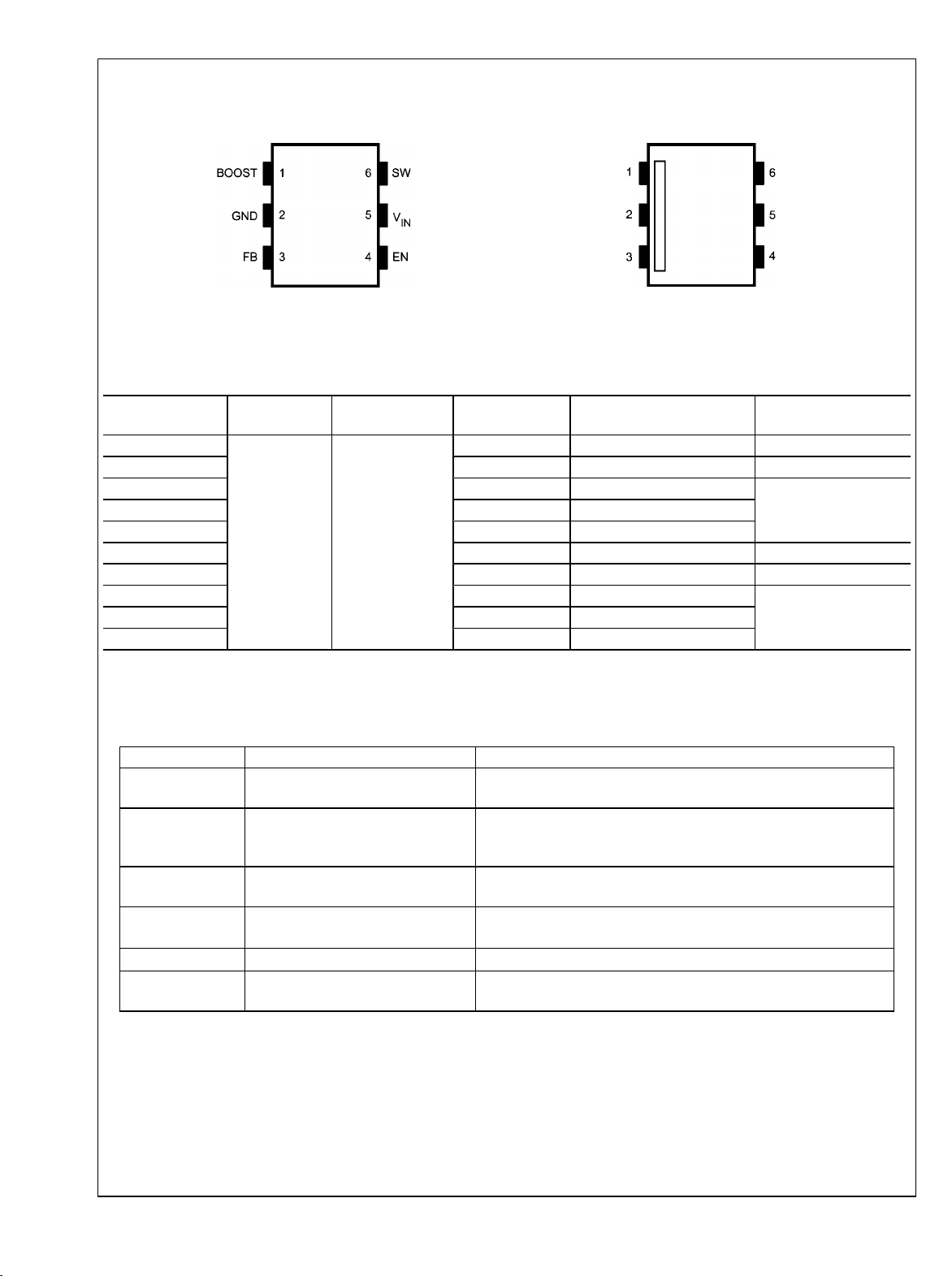
Connection Diagrams
LM2734
6-Lead TSOT
20102305
Pin 1 Indentification
20102360
NS Package Number MK06A
Ordering Information
Order Number Package Type NSC Package
Drawing
LM2734XMK
LM2734XMKX SFDB 3000 Units on Tape and Reel
LM2734XQMKE SUKB 250 Units on Tape and Reel AEC-Q100 Grade 1
LM2734XQMK SUKB 1000 Units on Tape and Reel
LM2734XQMKX SUKB 3000 Units on Tape and Reel
LM2734YMK SFEB 1000 Units on Tape and Reel
TSOT-6 MK06A
LM2734YMKX SFEB 3000 Units on Tape and Reel
LM2734YQMKE SVCB 250 Units on Tape and Reel AEC-Q10-0 Grade 1
LM2734YQMK SVCB 1000 Units on Tape and Reel
LM2734YQMKX SVCB 3000 Units on Tape and Reel
*Automotive Grade (Q) product incorporates enhanced manufacturing and support processes for the automotive market, including defect detection methodologies.
Reliability qualification is compliant with the requirements and temperature grades defined in the AEC-Q100 standard. Automotive grade products are identified
with the letter Q. For more information go to http://www.national.com/automotive.
Package
Supplied As Features
Marking
SFDB 1000 Units on Tape and Reel
Qualified. Automotive
Grade Production Flow*
Qualified. Automotive
Grade Production Flow*
Pin Descriptions
Pin Name Function
1 BOOST Boost voltage that drives the internal NMOS control switch. A
bootstrap capacitor is connected between the BOOST and SW pins.
2 GND Signal and Power ground pin. Place the bottom resistor of the
feedback network as close as possible to this pin for accurate
regulation.
3 FB Feedback pin. Connect FB to the external resistor divider to set output
voltage.
4 EN Enable control input. Logic high enables operation. Do not allow this
pin to float or be greater than V
5 V
IN
Input supply voltage. Connect a bypass capacitor to this pin.
6 SW Output switch. Connects to the inductor, catch diode, and bootstrap
capacitor.
+ 0.3V.
IN
www.national.com 2
LM2734
Absolute Maximum Ratings (Note 1)
If Military/Aerospace specified devices are required,
please contact the National Semiconductor Sales Office/
Distributors for availability and specifications.
V
IN
SW Voltage -0.5V to 24V
Boost Voltage -0.5V to 30V
Boost to SW Voltage -0.5V to 6.0V
FB Voltage -0.5V to 3.0V
EN Voltage -0.5V to (VIN + 0.3V)
Junction Temperature 150°C
ESD Susceptibility (Note 2) 2kV
-0.5V to 24V
Storage Temp. Range -65°C to 150°C
Soldering Information
Infrared/Convection Reflow (15sec) 220°C
Wave Soldering Lead Temp. (10sec) 260°C
Operating Ratings (Note 1)
V
IN
SW Voltage -0.5V to 20V
Boost Voltage -0.5V to 25V
Boost to SW Voltage 1.6V to 5.5V
Junction Temperature Range −40°C to +125°C
Thermal Resistance θJA (Note 3)
3V to 20V
118°C/W
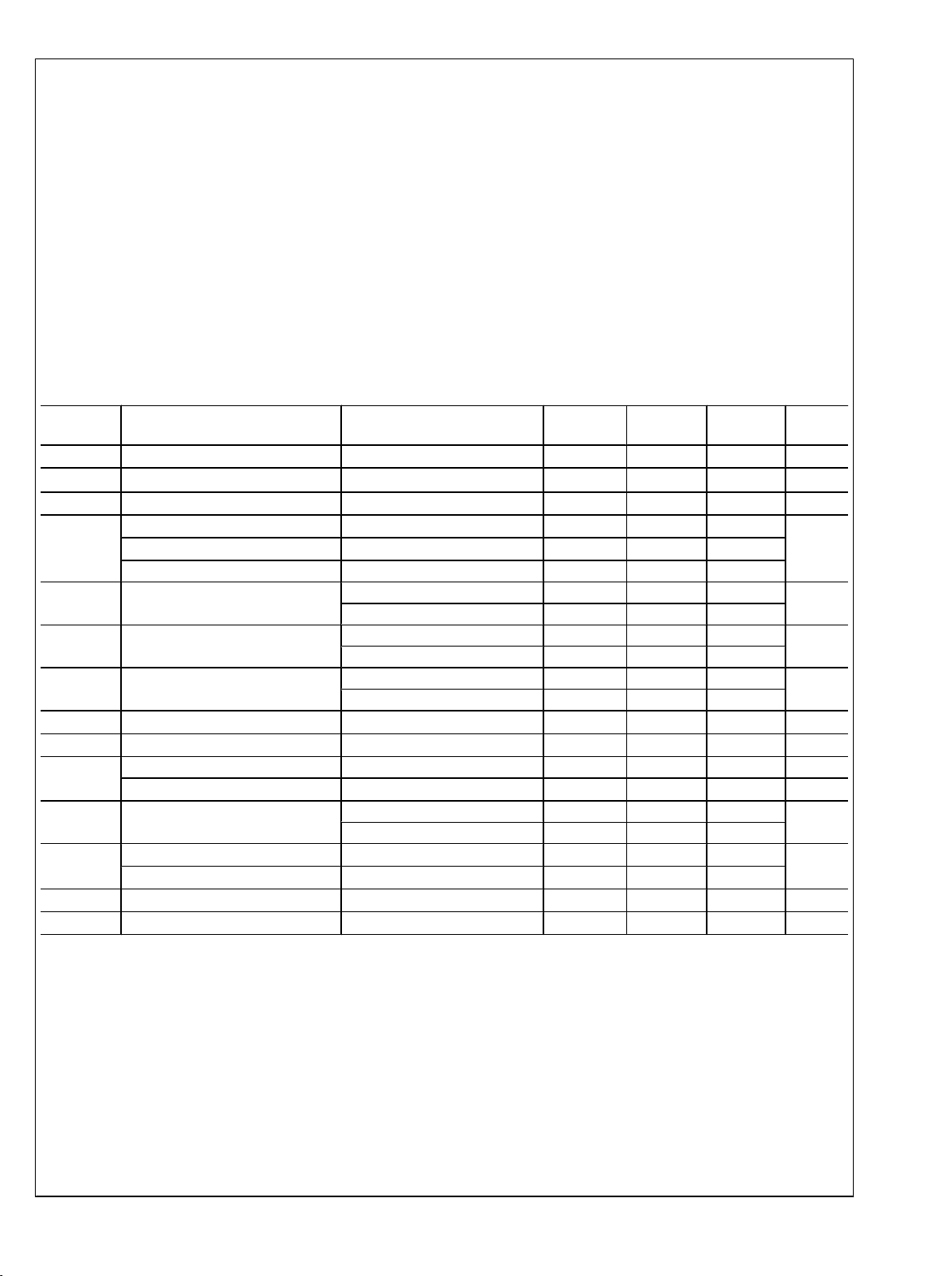
Electrical Characteristics
Specifications with standard typeface are for TJ = 25°C, and those in boldface type apply over the full Operating Temperature
Range (TJ = -40°C to 125°C). VIN = 5V, V
guaranteed by design, test, or statistical analysis.
Symbol Parameter Conditions
V
ΔVFB/ΔV
I
FB
Feedback Voltage
FB
Feedback Voltage Line Regulation
IN
Feedback Input Bias Current
Undervoltage Lockout
UVLO
Undervoltage Lockout
UVLO Hysteresis 0.30 0.44 0.62
F
D
D
R
DS(ON)
SW
MAX
MIN
I
CL
I
Switching Frequency
Maximum Duty Cycle
Minimum Duty Cycle
Switch ON Resistance V
Switch Current Limit V
Quiescent Current Switching 1.5 2.5 mA
Q
Quiescent Current (shutdown) VEN = 0V
I
BOOST
V
EN_TH
I
EN
I
SW
Note 1: Absolute Maximum Ratings indicate limits beyond which damage to the device may occur. Operating Ratings indicate conditions for which the device is
intended to be functional, but specific performance is not guaranteed. For guaranteed specifications and the test conditions, see Electrical Characteristics.
Note 2: Human body model, 1.5kΩ in series with 100pF.
Note 3: Thermal shutdown will occur if the junction temperature exceeds 165°C. The maximum power dissipation is a function of T
maximum allowable power dissipation at any ambient temperature is PD = (T
board with 2oz. copper on 4 layers in still air. For a 2 layer board using 1 oz. copper in still air, θJA = 204°C/W.
Note 4: Guaranteed to National’s Average Outgoing Quality Level (AOQL).
Note 5: Typicals represent the most likely parametric norm.
Boost Pin Current
Shutdown Threshold Voltage VEN Falling
Enable Threshold Voltage VEN Rising 1.8
Enable Pin Current Sink/Source
Switch Leakage
- VSW = 5V unless otherwise specified. Datasheet min/max specification limits are
BOOST
VIN = 3V to 20V
Sink/Source
VIN Rising
VIN Falling
Min
(Note 4)
0.784 0.800 0.816 V
0.01 % / V
10 250 nA
2.74 2.90
2.0 2.3
Typ
(Note 5)
Max
(Note 4)
LM2734X 1.2 1.6 1.9
LM2734Y 0.40 0.55 0.66
LM2734X 85 92
LM2734Y 90 96
LM2734X 2
LM2734Y 1
- VSW = 3V 300 600
BOOST
- VSW = 3V 1.2 1.7 2.5 A
BOOST
30
LM2734X (50% Duty Cycle) 2.5 3.5
LM2734Y (50% Duty Cycle) 1.0 1.8
0.4
– TA)/θJA . All numbers apply for packages soldered directly onto a 3” x 3” PC
J(MAX)
10
40
, θJA and TA . The
J(MAX)
Units
V
MHz
%
%
mΩ
nA
mA
V
nA
nA
3 www.national.com
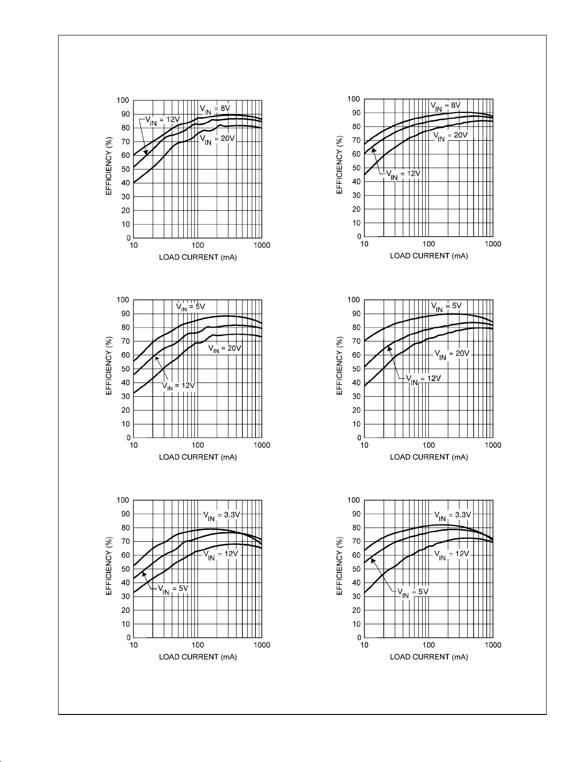
Typical Performance Characteristics All curves taken at V
L1 = 10 µH ("Y"), and TA = 25°C, unless specified otherwise.
LM2734
Efficiency vs Load Current - "X" V
OUT
= 5V
= 5V, V
IN
- VSW = 5V, L1 = 4.7 µH ("X"),
BOOST
Efficiency vs Load Current - "Y" V
OUT
= 5V
Efficiency vs Load Current - "X" V
Efficiency vs Load Current - "X" V
OUT
OUT
20102336
= 3.3V
20102351
= 1.5V
Efficiency vs Load Current - "Y" V
Efficiency vs Load Current - "Y" V
OUT
OUT
20102334
= 3.3V
20102352
= 1.5V
20102337
www.national.com 4
20102335
LM2734
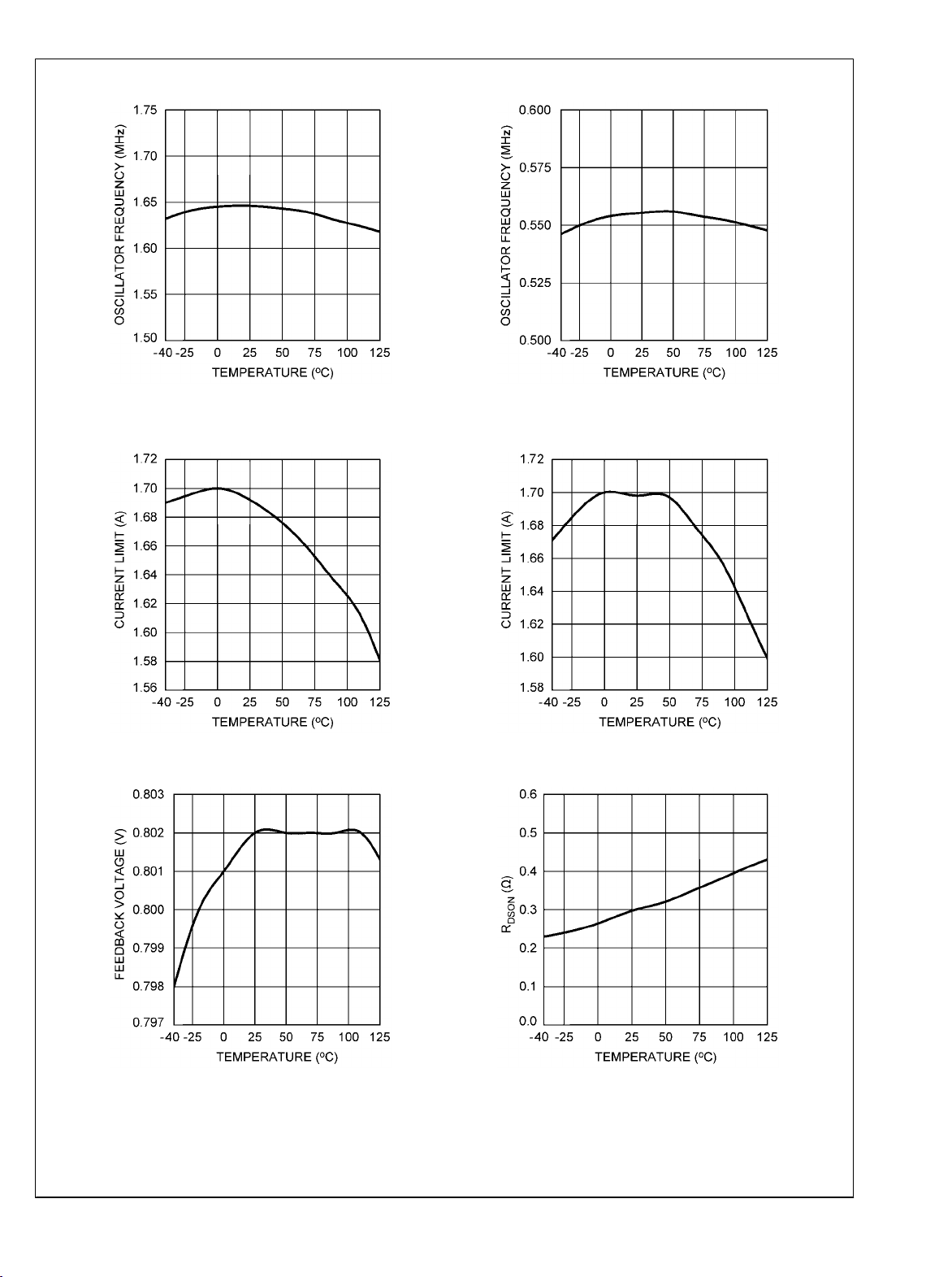
Oscillator Frequency vs Temperature - "X"
20102327
Current Limit vs Temperature
VIN = 5V
Oscillator Frequency vs Temperature - "Y"
20102328
Current Limit vs Temperature
VIN = 20V
VFB vs Temperature
20102329
20102333
20102347
R
vs Temperature
DSON
20102330
5 www.national.com
LM2734
IQ Switching vs Temperature
Line Regulation - "X"
V
OUT
= 1.5V, I
= 500mA
OUT
Line Regulation - "Y"
V
OUT
= 1.5V, I
= 500mA
OUT
Line Regulation - "Y"
V
OUT
= 3.3V, I
= 500mA
OUT
20102346
20102354
Line Regulation - "X"
V
OUT
= 3.3V, I
= 500mA
OUT
20102356
20102355
20102353
www.national.com 6
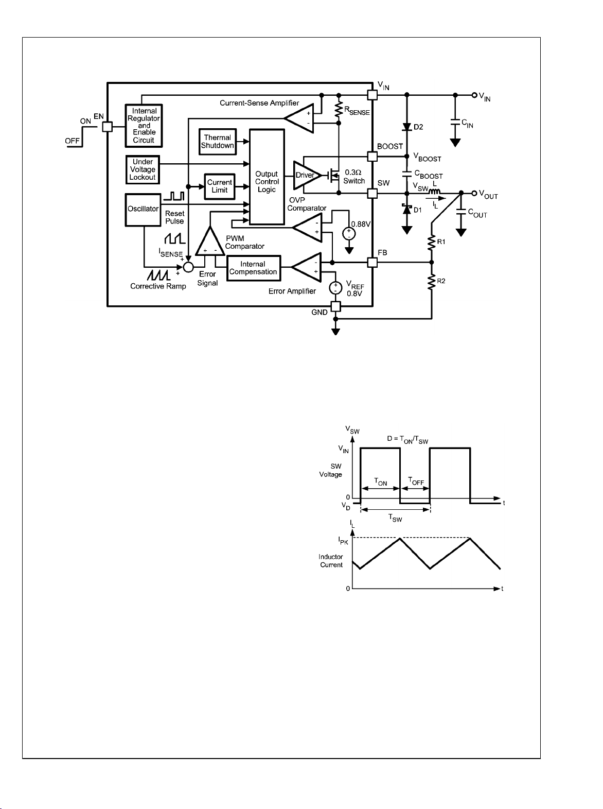
Block Diagram
LM2734
Application Information
THEORY OF OPERATION
The LM2734 is a constant frequency PWM buck regulator IC
that delivers a 1A load current. The regulator has a preset
switching frequency of either 550kHz (LM2734Y) or 1.6MHz
(LM2734X). These high frequencies allow the LM2734 to operate with small surface mount capacitors and inductors,
resulting in DC/DC converters that require a minimum amount
of board space. The LM2734 is internally compensated, so it
is simple to use, and requires few external components. The
LM2734 uses current-mode control to regulate the output
voltage.
The following operating description of the LM2734 will refer
to the Simplified Block Diagram (Figure 1) and to the waveforms in Figure 2. The LM2734 supplies a regulated output
voltage by switching the internal NMOS control switch at constant frequency and variable duty cycle. A switching cycle
begins at the falling edge of the reset pulse generated by the
internal oscillator. When this pulse goes low, the output control logic turns on the internal NMOS control switch. During
this on-time, the SW pin voltage (VSW) swings up to approximately VIN, and the inductor current (IL) increases with a linear
slope. IL is measured by the current-sense amplifier, which
generates an output proportional to the switch current. The
sense signal is summed with the regulator’s corrective ramp
and compared to the error amplifier’s output, which is proportional to the difference between the feedback voltage and
V
. When the PWM comparator output goes high, the out-
REF
put switch turns off until the next switching cycle begins.
During the switch off-time, inductor current discharges
through Schottky diode D1, which forces the SW pin to swing
below ground by the forward voltage (VD) of the catch diode.
FIGURE 1.
20102306
The regulator loop adjusts the duty cycle (D) to maintain a
constant output voltage.
20102307
FIGURE 2. LM2734 Waveforms of SW Pin Voltage and
Inductor Current
BOOST FUNCTION
Capacitor C
erate a voltage V
to the internal NMOS control switch. To properly drive the internal NMOS switch during its on-time, V
least 1.6V greater than VSW. Although the LM2734 will oper-
and diode D2 in Figure 3 are used to gen-
BOOST
BOOST
. V
- VSW is the gate drive voltage
BOOST
needs to be at
BOOST
ate with this minimum voltage, it may not have sufficient gate
drive to supply large values of output current. Therefore, it is
recommended that V
be greater than 2.5V above V
BOOST
SW
7 www.national.com
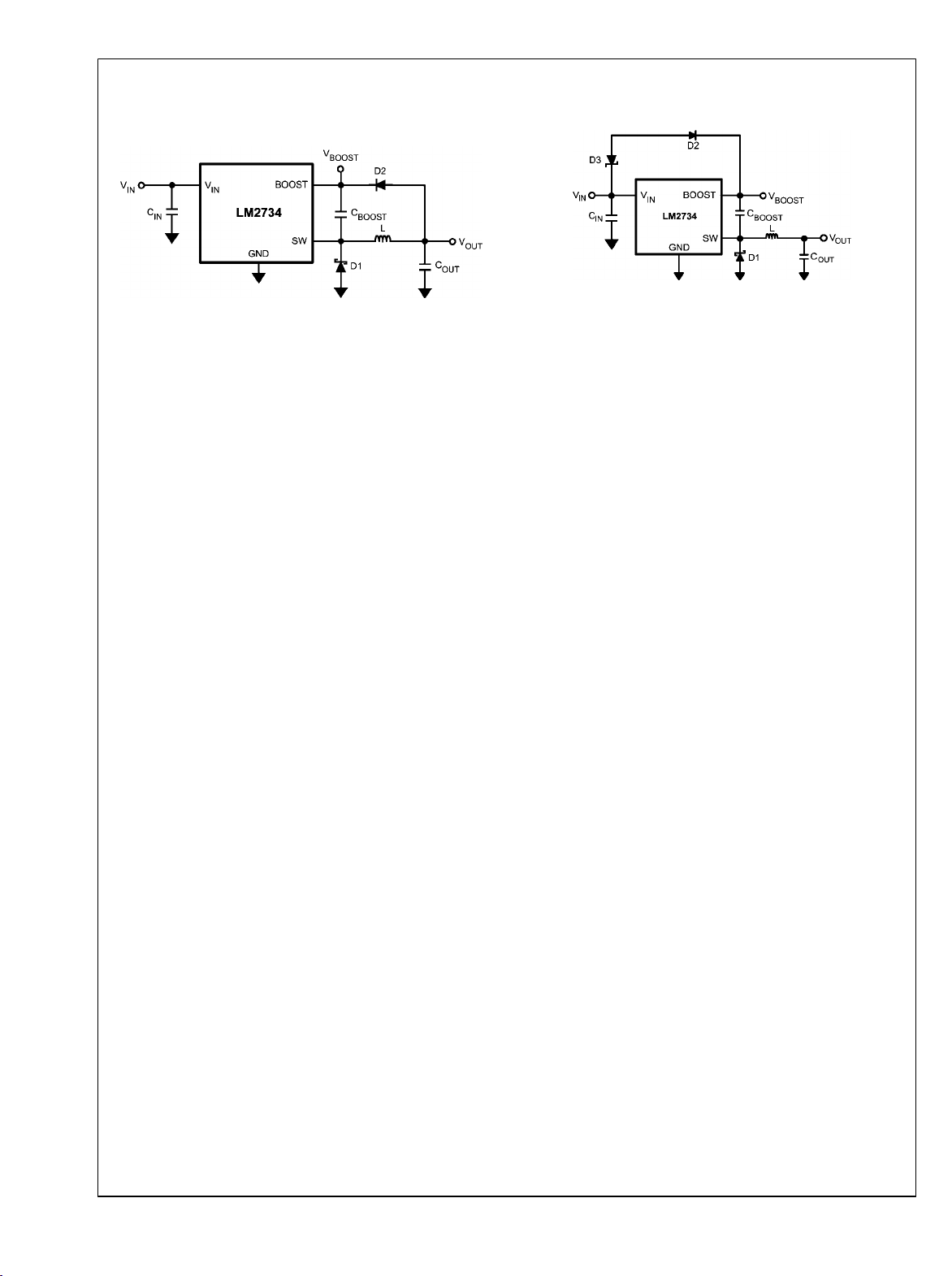
for best efficiency. V
imum operating limit of 5.5V.
LM2734
5.5V > V
– VSW > 2.5V for best performance.
BOOST
FIGURE 3. V
– VSW should not exceed the max-
BOOST
Charges C
OUT
BOOST
When the LM2734 starts up, internal circuitry from the
BOOST pin supplies a maximum of 20mA to C
current charges C
switch on. The BOOST pin will continue to source current to
C
until the voltage at the feedback pin is greater than
BOOST
0.76V.
There are various methods to derive V
1.
From the input voltage (VIN)
2.
From the output voltage (V
3.
From an external distributed voltage rail (V
4.
From a shunt or series zener diode
to a voltage sufficient to turn the
BOOST
:
BOOST
)
OUT
In the Simplifed Block Diagram of Figure 1, capacitor
C
and diode D2 supply the gate-drive current for the
BOOST
NMOS switch. Capacitor C
VIN. During a normal switching cycle, when the internal NMOS
control switch is off (T
VIN minus the forward voltage of D2 (V
OFF
current in the inductor (L) forward biases the Schottky diode
D1 (V
). Therefore the voltage stored across C
FD1
V
- VSW = VIN - V
BOOST
is charged via diode D2 by
BOOST
) (refer to Figure 2), V
), during which the
FD2
+ V
FD2
FD1
When the NMOS switch turns on (TON), the switch pin rises
to
forcing V
V
BOOST
VSW = VIN – (R
to rise thus reverse biasing D2. The voltage at
BOOST
is then
V
= 2VIN – (R
BOOST
DSON
x IL),
DSON
x IL) – V
FD2
+ V
which is approximately
2VIN - 0.4V
for many applications. Thus the gate-drive voltage of the
NMOS switch is approximately
VIN - 0.2V
An alternate method for charging C
the output as shown in Figure 3. The output voltage should
is to connect D2 to
BOOST
be between 2.5V and 5.5V, so that proper gate voltage will be
applied to the internal switch. In this circuit, C
a gate drive voltage that is slightly less than V
In applications where both VIN and V
5.5V, or less than 3V, C
these voltages. If VIN and V
C
can be charged from VIN or V
BOOST
age by placing a zener diode D3 in series with D2, as shown
cannot be charged directly from
BOOST
are greater than 5.5V,
OUT
OUT
BOOST
OUT
are greater than
OUT
minus a zener volt-
in Figure 4. When using a series zener diode from the input,
ensure that the regulation of the input supply doesn’t create
a voltage that falls outside the recommended V
BOOST
BOOST
)
EXT
BOOST
BOOST
FD1
.
20102308
. This
equals
is
provides
voltage.
(V
– VD3) < 5.5V
INMAX
(V
– VD3) > 1.6V
INMIN
20102309
FIGURE 4. Zener Reduces Boost Voltage from V
IN
An alternative method is to place the zener diode D3 in a
shunt configuration as shown in Figure 5. A small 350mW to
500mW 5.1V zener in a SOT-23 or SOD package can be used
for this purpose. A small ceramic capacitor such as a 6.3V,
0.1µF capacitor (C4) should be placed in parallel with the
zener diode. When the internal NMOS switch turns on, a pulse
of current is drawn to charge the internal NMOS gate capacitance. The 0.1 µF parallel shunt capacitor ensures that the
V
voltage is maintained during this time.
BOOST
Resistor R3 should be chosen to provide enough RMS current
to the zener diode (D3) and to the BOOST pin. A recommended choice for the zener current (I
current I
of the NMOS control switch and varies typically according to
into the BOOST pin supplies the gate current
BOOST
) is 1 mA. The
ZENER
the following formula for the X version:
I
= 0.56 x (D + 0.54) x (V
BOOST
I
can be calculated for the Y version using the following:
BOOST
I
= 0.22 x (D + 0.54) x (V
BOOST
where D is the duty cycle, V
I
is in milliamps. V
BOOST
anode of the boost diode (D2), and VD2 is the average forward
ZENER
and VD2 are in volts, and
ZENER
is the voltage applied to the
voltage across D2. Note that this formula for I
ical current. For the worst case I
by 40%. In that case, the worst case boost current will be
I
BOOST-MAX
BOOST
= 1.4 x I
– VD2) mA
ZENER
- VD2) µA
ZENER
gives typ-
BOOST
, increase the current
BOOST
R3 will then be given by
R3 = (VIN - V
For example, using the X-version let VIN = 10V, V
VD2 = 0.7V, I
I
BOOST
= 1mA, and duty cycle D = 50%. Then
ZENER
= 0.56 x (0.5 + 0.54) x (5 - 0.7) mA = 2.5mA
ZENER
) / (1.4 x I
BOOST
+ I
ZENER
ZENER
)
= 5V,
R3 = (10V - 5V) / (1.4 x 2.5mA + 1mA) = 1.11kΩ
www.national.com 8

doesn’t turn on until the junction temperature drops to approximately 150°C.
Design Guide
INDUCTOR SELECTION
The Duty Cycle (D) can be approximated quickly using the
ratio of output voltage (VO) to input voltage (VIN):
LM2734
20102348
FIGURE 5. Boost Voltage Supplied from the Shunt Zener
on V
IN
ENABLE PIN / SHUTDOWN MODE
The LM2734 has a shutdown mode that is controlled by the
enable pin (EN). When a logic low voltage is applied to EN,
the part is in shutdown mode and its quiescent current drops
to typically 30nA. Switch leakage adds another 40nA from the
input supply. The voltage at this pin should never exceed
VIN + 0.3V.
SOFT-START
This function forces V
ing start up. During soft-start, the error amplifier’s reference
to increase at a controlled rate dur-
OUT
voltage ramps from 0V to its nominal value of 0.8V in approximately 200µs. This forces the regulator output to ramp up in
a more linear and controlled fashion, which helps reduce inrush current. Under some circumstances at start-up, an output voltage overshoot may still be observed. This may be due
to a large output load applied during start up. Large amounts
of output external capacitance can also increase output voltage overshoot. A simple solution is to add a feed forward
capacitor with a value between 470pf and 1000pf across the
top feedback resistor (R1). See Figure 7 for further detail.
OUTPUT OVERVOLTAGE PROTECTION
The overvoltage comparator compares the FB pin voltage to
a voltage that is 10% higher than the internal reference Vref.
Once the FB pin voltage goes 10% above the internal reference, the internal NMOS control switch is turned off, which
allows the output voltage to decrease toward regulation.
UNDERVOLTAGE LOCKOUT
Undervoltage lockout (UVLO) prevents the LM2734 from operating until the input voltage exceeds 2.74V(typ).
The UVLO threshold has approximately 440mV of hysteresis,
so the part will operate until VIN drops below 2.3V(typ). Hysteresis prevents the part from turning off during power up if
VIN is non-monotonic.
CURRENT LIMIT
The LM2734 uses cycle-by-cycle current limiting to protect
the output switch. During each switching cycle, a current limit
comparator detects if the output switch current exceeds 1.7A
(typ), and turns off the switch until the next switching cycle
begins.
THERMAL SHUTDOWN
Thermal shutdown limits total power dissipation by turning off
the output switch when the IC junction temperature exceeds
165°C. After thermal shutdown occurs, the output switch
The catch diode (D1) forward voltage drop and the voltage
drop across the internal NMOS must be included to calculate
a more accurate duty cycle. Calculate D by using the following
formula:
VSW can be approximated by:
VSW = IO x R
DS(ON)
The diode forward drop (VD) can range from 0.3V to 0.7V depending on the quality of the diode. The lower VD is, the higher
the operating efficiency of the converter.
The inductor value determines the output ripple current. Lower inductor values decrease the size of the inductor, but
increase the output ripple current. An increase in the inductor
value will decrease the output ripple current. The ratio of ripple
current (ΔiL) to output current (IO) is optimized when it is set
between 0.3 and 0.4 at 1A. The ratio r is defined as:
One must also ensure that the minimum current limit (1.2A)
is not exceeded, so the peak current in the inductor must be
calculated. The peak current (I
by:
I
LPK
) in the inductor is calculated
LPK
= IO + ΔIL/2
If r = 0.5 at an output of 1A, the peak current in the inductor
will be 1.25A. The minimum guaranteed current limit over all
operating conditions is 1.2A. One can either reduce r to 0.4
resulting in a 1.2A peak current, or make the engineering
judgement that 50mA over will be safe enough with a 1.7A
typical current limit and 6 sigma limits. When the designed
maximum output current is reduced, the ratio r can be increased. At a current of 0.1A, r can be made as high as 0.9.
The ripple ratio can be increased at lighter loads because the
net ripple is actually quite low, and if r remains constant the
inductor value can be made quite large. An equation empirically developed for the maximum ripple ratio at any current
below 2A is:
r = 0.387 x I
OUT
-0.3667
Note that this is just a guideline.
The LM2734 operates at frequencies allowing the use of ce-
ramic output capacitors without compromising transient response. Ceramic capacitors allow higher inductor ripple
without significantly increasing output ripple. See the output
9 www.national.com

capacitor section for more details on calculating output voltage ripple.
LM2734
Now that the ripple current or ripple ratio is determined, the
inductance is calculated by:
OUTPUT CAPACITOR
The output capacitor is selected based upon the desired output ripple and transient response. The initial current of a load
transient is provided mainly by the output capacitor. The output ripple of the converter is:
where fs is the switching frequency and IO is the output current. When selecting an inductor, make sure that it is capable
of supporting the peak output current without saturating. Inductor saturation will result in a sudden reduction in inductance and prevent the regulator from operating correctly.
Because of the speed of the internal current limit, the peak
current of the inductor need only be specified for the required
maximum output current. For example, if the designed maximum output current is 0.5A and the peak current is 0.7A, then
the inductor should be specified with a saturation current limit
of >0.7A. There is no need to specify the saturation or peak
current of the inductor at the 1.7A typical switch current limit.
The difference in inductor size is a factor of 5. Because of the
operating frequency of the LM2734, ferrite based inductors
are preferred to minimize core losses. This presents little restriction since the variety of ferrite based inductors is huge.
Lastly, inductors with lower series resistance (DCR) will provide better operating efficiency. For recommended inductors
see Example Circuits.
INPUT CAPACITOR
An input capacitor is necessary to ensure that VIN does not
drop excessively during switching transients. The primary
specifications of the input capacitor are capacitance, voltage,
RMS current rating, and ESL (Equivalent Series Inductance).
The recommended input capacitance is 10µF, although 4.7µF
works well for input voltages below 6V. The input voltage rating is specifically stated by the capacitor manufacturer. Make
sure to check any recommended deratings and also verify if
there is any significant change in capacitance at the operating
input voltage and the operating temperature. The input capacitor maximum RMS input current rating (I
greater than:
RMS-IN
) must be
It can be shown from the above equation that maximum RMS
capacitor current occurs when D = 0.5. Always calculate the
RMS at the point where the duty cycle, D, is closest to 0.5.
The ESL of an input capacitor is usually determined by the
effective cross sectional area of the current path. A large
leaded capacitor will have high ESL and a 0805 ceramic chip
capacitor will have very low ESL. At the operating frequencies
of the LM2734, certain capacitors may have an ESL so large
that the resulting impedance (2πfL) will be higher than that
required to provide stable operation. As a result, surface
mount capacitors are strongly recommended. Sanyo
POSCAP, Tantalum or Niobium, Panasonic SP or Cornell
Dubilier ESR, and multilayer ceramic capacitors (MLCC) are
all good choices for both input and output capacitors and have
very low ESL. For MLCCs it is recommended to use X7R or
X5R dielectrics. Consult capacitor manufacturer datasheet to
see how rated capacitance varies over operating conditions.
When using MLCCs, the ESR is typically so low that the capacitive ripple may dominate. When this occurs, the output
ripple will be approximately sinusoidal and 90° phase shifted
from the switching action. Given the availability and quality of
MLCCs and the expected output voltage of designs using the
LM2734, there is really no need to review any other capacitor
technologies. Another benefit of ceramic capacitors is their
ability to bypass high frequency noise. A certain amount of
switching edge noise will couple through parasitic capacitances in the inductor to the output. A ceramic capacitor will
bypass this noise while a tantalum will not. Since the output
capacitor is one of the two external components that control
the stability of the regulator control loop, most applications will
require a minimum at 10 µF of output capacitance. Capacitance can be increased significantly with little detriment to the
regulator stability. Like the input capacitor, recommended
multilayer ceramic capacitors are X7R or X5R. Again, verify
actual capacitance at the desired operating voltage and temperature.
Check the RMS current rating of the capacitor. The RMS current rating of the capacitor chosen must also meet the following condition:
CATCH DIODE
The catch diode (D1) conducts during the switch off-time. A
Schottky diode is recommended for its fast switching times
and low forward voltage drop. The catch diode should be
chosen so that its current rating is greater than:
ID1 = IO x (1-D)
The reverse breakdown rating of the diode must be at least
the maximum input voltage plus appropriate margin. To improve efficiency choose a Schottky diode with a low forward
voltage drop.
BOOST DIODE
A standard diode such as the 1N4148 type is recommended.
For V
small-signal Schottky diode is recommended for greater effi-
circuits derived from voltages less than 3.3V, a
BOOST
ciency. A good choice is the BAT54 small signal diode.
BOOST CAPACITOR
A ceramic 0.01µF capacitor with a voltage rating of at least
6.3V is sufficient. The X7R and X5R MLCCs provide the best
performance.
OUTPUT VOLTAGE
The output voltage is set using the following equation where
R2 is connected between the FB pin and GND, and R1 is
connected between VO and the FB pin. A good value for R2
is 10kΩ.
www.national.com 10

PCB Layout Considerations
When planning layout there are a few things to consider when
trying to achieve a clean, regulated output. The most important consideration when completing the layout is the close
coupling of the GND connections of the CIN capacitor and the
catch diode D1. These ground ends should be close to one
another and be connected to the GND plane with at least two
through-holes. Place these components as close to the IC as
possible. Next in importance is the location of the GND connection of the C
connections of CIN and D1.
There should be a continuous ground plane on the bottom
layer of a two-layer board except under the switching node
island.
capacitor, which should be near the GND
OUT
The FB pin is a high impedance node and care should be
taken to make the FB trace short to avoid noise pickup and
inaccurate regulation. The feedback resistors should be
placed as close as possible to the IC, with the GND of R2
placed as close as possible to the GND of the IC. The V
trace to R1 should be routed away from the inductor and any
OUT
other traces that are switching.
High AC currents flow through the VIN, SW and V
so they should be as short and wide as possible. However,
OUT
traces,
making the traces wide increases radiated noise, so the designer must make this trade-off. Radiated noise can be decreased by choosing a shielded inductor.
The remaining components should also be placed as close
as possible to the IC. Please see Application Note AN-1229
for further considerations and the LM2734 demo board as an
example of a four-layer layout.
LM2734
11 www.national.com

LM2734X Circuit Examples
LM2734
FIGURE 6. LM2734X (1.6MHz)
V
Derived from V
BOOST
5V to 1.5V/1A
IN
Bill of Materials for Figure 6
20102342
Part ID Part Value Part Number Manufacturer
U1 1A Buck Regulator LM2734X National Semiconductor
C1, Input Cap 10µF, 6.3V, X5R C3216X5ROJ106M TDK
C2, Output Cap 10µF, 6.3V, X5R C3216X5ROJ106M TDK
C3, Boost Cap 0.01uF, 16V, X7R C1005X7R1C103K TDK
D1, Catch Diode 0.3VF Schottky 1A, 10VR MBRM110L ON Semi
D2, Boost Diode 1VF @ 50mA Diode 1N4148W Diodes, Inc.
L1 4.7µH, 1.7A, VLCF4020T- 4R7N1R2 TDK
R1
R2
R3
8.87kΩ, 1%
10.2kΩ, 1%
100kΩ, 1%
CRCW06038871F Vishay
CRCW06031022F Vishay
CRCW06031003F Vishay
www.national.com 12

20102343
FIGURE 7. LM2734X (1.6MHz)
V
Derived from V
BOOST
12V to 3.3V/1A
OUT
Bill of Materials for Figure 7
Part ID Part Value Part Number Manufacturer
U1 1A Buck Regulator NSC LM2734X
C1, Input Cap 10µF, 25V, X7R C3225X7R1E106M TDK
C2, Output Cap 22µF, 6.3V, X5R C3216X5ROJ226M TDK
C3, Boost Cap 0.01µF, 16V, X7R C1005X7R1C103K TDK
CFF 1000pF 25V C0603X5R1E102K TDK
D1, Catch Diode 0.34VF Schottky 1A, 30VR SS1P3L Vishay
D2, Boost Diode 1VF @ 50mA Diode 1N4148W Diodes, Inc.
L1 4.7µH, 1.7A VLCF4020T- 4R7N1R2 TDK
R1
R2
R3
31.6kΩ, 1%
10kΩ, 1%
100kΩ, 1%
CRCW06033162F Vishay
CRCW06031002F Vishay
CRCW06031003F Vishay
LM2734
13 www.national.com

LM2734
20102344
FIGURE 8. LM2734X (1.6MHz)
V
Derived from V
BOOST
18V to 1.5V/1A
Bill of Materials for Figure 8
Part ID Part Value Part Number Manufacturer
U1 1A Buck Regulator LM2734X National Semiconductor
C1, Input Cap 10µF, 25V, X7R C3225X7R1E106M TDK
C2, Output Cap 22µF, 6.3V, X5R C3216X5ROJ226M TDK
C3, Boost Cap 0.01µF, 16V, X7R C1005X7R1C103K TDK
C4, Shunt Cap 0.1µF, 6.3V, X5R C1005X5R0J104K TDK
D1, Catch Diode 0.4VF Schottky 1A, 30VR SS1P3L Vishay
D2, Boost Diode 1VF @ 50mA Diode 1N4148W Diodes, Inc.
D3, Zener Diode 5.1V 250Mw SOT-23 BZX84C5V1 Vishay
L1 6.8µH, 1.6A, SLF7032T-6R8M1R6 TDK
R1
R2
R3
R4
8.87kΩ, 1%
10.2kΩ, 1%
100kΩ, 1%
4.12kΩ, 1%
CRCW06038871F Vishay
CRCW06031022F Vishay
CRCW06031003F Vishay
CRCW06034121F Vishay
SHUNT
www.national.com 14

20102349
LM2734
V
Derived from Series Zener Diode (VIN)
BOOST
15V to 1.5V/1A
Bill of Materials for Figure 9
Part ID Part Value Part Number Manufacturer
U1 1A Buck Regulator LM2734X National Semiconductor
C1, Input Cap 10µF, 25V, X7R C3225X7R1E106M TDK
C2, Output Cap 22µF, 6.3V, X5R C3216X5ROJ226M TDK
C3, Boost Cap 0.01µF, 16V, X7R C1005X7R1C103K TDK
D1, Catch Diode 0.4VF Schottky 1A, 30VR SS1P3L Vishay
D2, Boost Diode 1VF @ 50mA Diode 1N4148W Diodes, Inc.
D3, Zener Diode 11V 350Mw SOT-23 BZX84C11T Diodes, Inc.
L1 6.8µH, 1.6A, SLF7032T-6R8M1R6 TDK
FIGURE 9. LM2734X (1.6MHz)
R1
R2
R3
8.87kΩ, 1%
10.2kΩ, 1%
100kΩ, 1%
CRCW06038871F Vishay
CRCW06031022F Vishay
CRCW06031003F Vishay
15 www.national.com

LM2734
20102350
V
Derived from Series Zener Diode (V
BOOST
15V to 9V/1A
OUT
)
Bill of Materials for Figure 10
Part ID Part Value Part Number Manufacturer
U1 1A Buck Regulator LM2734X National Semiconductor
C1, Input Cap 10µF, 25V, X7R C3225X7R1E106M TDK
C2, Output Cap 22µF, 16V, X5R C3216X5R1C226M TDK
C3, Boost Cap 0.01µF, 16V, X7R C1005X7R1C103K TDK
D1, Catch Diode 0.4VF Schottky 1A, 30VR SS1P3L Vishay
D2, Boost Diode 1VF @ 50mA Diode 1N4148W Diodes, Inc.
D3, Zener Diode 4.3V 350mw SOT-23 BZX84C4V3 Diodes, Inc.
L1 6.8µH, 1.6A, SLF7032T-6R8M1R6 TDK
FIGURE 10. LM2734X (1.6MHz)
R1
R2
R3
102kΩ, 1%
10.2kΩ, 1%
100kΩ, 1%
CRCW06031023F Vishay
CRCW06031022F Vishay
CRCW06031003F Vishay
www.national.com 16

LM2734Y Circuit Examples
FIGURE 11. LM2734Y (550kHz)
V
Derived from V
BOOST
5V to 1.5V/1A
IN
LM2734
20102342
Bill of Materials for Figure 11
Part ID Part Value Part Number Manufacturer
U1 1A Buck Regulator LM2734Y National Semiconductor
C1, Input Cap 10µF, 6.3V, X5R C3216X5ROJ106M TDK
C2, Output Cap 22µF, 6.3V, X5R C3216X5ROJ226M TDK
C3, Boost Cap 0.01µF, 16V, X7R C1005X7R1C103K TDK
D1, Catch Diode 0.3VF Schottky 1A, 10VR MBRM110L ON Semi
D2, Boost Diode 1VF @ 50mA Diode 1N4148W Diodes, Inc.
L1 10µH, 1.6A, SLF7032T-100M1R4 TDK
R1
R2
R3
8.87kΩ, 1%
10.2kΩ, 1%
100kΩ, 1%
CRCW06038871F Vishay
CRCW06031022F Vishay
CRCW06031003F Vishay
17 www.national.com

LM2734
20102343
FIGURE 12. LM2734Y (550kHz)
V
Derived from V
BOOST
12V to 3.3V/1A
Bill of Materials for Figure 12
Part ID Part Value Part Number Manufacturer
U1 1A Buck Regulator LM2734Y National Semiconductor
C1, Input Cap 10µF, 25V, X7R C3225X7R1E106M TDK
C2, Output Cap 22µF, 6.3V, X5R C3216X5ROJ226M TDK
C3, Boost Cap 0.01µF, 16V, X7R C1005X7R1C103K TDK
D1, Catch Diode 0.34VF Schottky 1A, 30VR SS1P3L Vishay
D2, Boost Diode 0.6VF @ 30mA Diode BAT17 Vishay
L1 10µH, 1.6A, SLF7032T-100M1R4 TDK
R1
R2
R3
31.6kΩ, 1%
10.0 kΩ, 1%
100kΩ, 1%
CRCW06033162F Vishay
CRCW06031002F Vishay
CRCW06031003F Vishay
OUT
www.national.com 18

FIGURE 13. LM2734Y (550kHz)
V
Derived from V
BOOST
18V to 1.5V/1A
SHUNT
LM2734
20102344
Bill of Materials for Figure 13
Part ID Part Value Part Number Manufacturer
U1 1A Buck Regulator LM2734Y National Semiconductor
C1, Input Cap 10µF, 25V, X7R C3225X7R1E106M TDK
C2, Output Cap 22µF, 6.3V, X5R C3216X5ROJ226M TDK
C3, Boost Cap 0.01µF, 16V, X7R C1005X7R1C103K TDK
C4, Shunt Cap 0.1µF, 6.3V, X5R C1005X5R0J104K TDK
D1, Catch Diode 0.4VF Schottky 1A, 30VR SS1P3L Vishay
D2, Boost Diode 1VF @ 50mA Diode 1N4148W Diodes, Inc.
D3, Zener Diode 5.1V 250Mw SOT-23 BZX84C5V1 Vishay
L1 15µH, 1.5A SLF7045T-150M1R5 TDK
R1
R2
R3
R4
8.87kΩ, 1%
10.2kΩ, 1%
100kΩ, 1%
4.12kΩ, 1%
CRCW06038871F Vishay
CRCW06031022F Vishay
CRCW06031003F Vishay
CRCW06034121F Vishay
19 www.national.com

LM2734
20102349
FIGURE 14. LM2734Y (550kHz)
V
Derived from Series Zener Diode (VIN)
BOOST
Part ID Part Value Part Number Manufacturer
U1 1A Buck Regulator LM2734Y National Semiconductor
C1, Input Cap 10µF, 25V, X7R C3225X7R1E106M TDK
C2, Output Cap 22µF, 6.3V, X5R C3216X5ROJ226M TDK
C3, Boost Cap 0.01µF, 16V, X7R C1005X7R1C103K TDK
D1, Catch Diode 0.4VF Schottky 1A, 30VR SS1P3L Vishay
D2, Boost Diode 1VF @ 50mA Diode 1N4148W Diodes, Inc.
D3, Zener Diode 11V 350Mw SOT-23 BZX84C11T Diodes, Inc.
L1 15µH, 1.5A, SLF7045T-150M1R5 TDK
R1
R2
R3
8.87kΩ, 1%
10.2kΩ, 1%
100kΩ, 1%
15V to 1.5V/1A
Bill of Materials for Figure 14
CRCW06038871F Vishay
CRCW06031022F Vishay
CRCW06031003F Vishay
www.national.com 20

20102350
LM2734
V
Derived from Series Zener Diode (V
BOOST
15V to 9V/1A
OUT
)
Bill of Materials for Figure 15
Part ID Part Value Part Number Manufacturer
U1 1A Buck Regulator LM2734Y National Semiconductor
C1, Input Cap 10µF, 25V, X7R C3225X7R1E106M TDK
C2, Output Cap 22µF, 16V, X5R C3216X5R1C226M TDK
C3, Boost Cap 0.01µF, 16V, X7R C1005X7R1C103K TDK
D1, Catch Diode 0.4VF Schottky 1A, 30VR SS1P3L Vishay
D2, Boost Diode 1VF @ 50mA Diode 1N4148W Diodes, Inc.
D3, Zener Diode 4.3V 350mw SOT-23 BZX84C4V3 Diodes, Inc.
L1 22µH, 1.4A, SLF7045T-220M1R3-1PF TDK
FIGURE 15. LM2734Y (550kHz)
R1
R2
R3
102kΩ, 1%
10.2kΩ, 1%
100kΩ, 1%
CRCW06031023F Vishay
CRCW06031022F Vishay
CRCW06031003F Vishay
21 www.national.com

Physical Dimensions inches (millimeters) unless otherwise noted
LM2734
6-Lead TSOT Package
NS Package Number MK06A
www.national.com 22

Notes
LM2734
23 www.national.com

Notes
For more National Semiconductor product information and proven design tools, visit the following Web sites at:
Products Design Support
Amplifiers www.national.com/amplifiers WEBENCH www.national.com/webench
Audio www.national.com/audio Analog University www.national.com/AU
Clock Conditioners www.national.com/timing App Notes www.national.com/appnotes
Data Converters www.national.com/adc Distributors www.national.com/contacts
Displays www.national.com/displays Green Compliance www.national.com/quality/green
Ethernet www.national.com/ethernet Packaging www.national.com/packaging
Interface www.national.com/interface Quality and Reliability www.national.com/quality
LVDS www.national.com/lvds Reference Designs www.national.com/refdesigns
Power Management www.national.com/power Feedback www.national.com/feedback
Switching Regulators www.national.com/switchers
LDOs www.national.com/ldo
LED Lighting www.national.com/led
PowerWise www.national.com/powerwise
Serial Digital Interface (SDI) www.national.com/sdi
Temperature Sensors www.national.com/tempsensors
Wireless (PLL/VCO) www.national.com/wireless
THE CONTENTS OF THIS DOCUMENT ARE PROVIDED IN CONNECTION WITH NATIONAL SEMICONDUCTOR CORPORATION
(“NATIONAL”) PRODUCTS. NATIONAL MAKES NO REPRESENTATIONS OR WARRANTIES WITH RESPECT TO THE ACCURACY
OR COMPLETENESS OF THE CONTENTS OF THIS PUBLICATION AND RESERVES THE RIGHT TO MAKE CHANGES TO
SPECIFICATIONS AND PRODUCT DESCRIPTIONS AT ANY TIME WITHOUT NOTICE. NO LICENSE, WHETHER EXPRESS,
IMPLIED, ARISING BY ESTOPPEL OR OTHERWISE, TO ANY INTELLECTUAL PROPERTY RIGHTS IS GRANTED BY THIS
DOCUMENT.
TESTING AND OTHER QUALITY CONTROLS ARE USED TO THE EXTENT NATIONAL DEEMS NECESSARY TO SUPPORT
NATIONAL’S PRODUCT WARRANTY. EXCEPT WHERE MANDATED BY GOVERNMENT REQUIREMENTS, TESTING OF ALL
PARAMETERS OF EACH PRODUCT IS NOT NECESSARILY PERFORMED. NATIONAL ASSUMES NO LIABILITY FOR
LM2734 Thin SOT23 1A Load Step-Down DC-DC Regulator
APPLICATIONS ASSISTANCE OR BUYER PRODUCT DESIGN. BUYERS ARE RESPONSIBLE FOR THEIR PRODUCTS AND
APPLICATIONS USING NATIONAL COMPONENTS. PRIOR TO USING OR DISTRIBUTING ANY PRODUCTS THAT INCLUDE
NATIONAL COMPONENTS, BUYERS SHOULD PROVIDE ADEQUATE DESIGN, TESTING AND OPERATING SAFEGUARDS.
EXCEPT AS PROVIDED IN NATIONAL’S TERMS AND CONDITIONS OF SALE FOR SUCH PRODUCTS, NATIONAL ASSUMES NO
LIABILITY WHATSOEVER, AND NATIONAL DISCLAIMS ANY EXPRESS OR IMPLIED WARRANTY RELATING TO THE SALE
AND/OR USE OF NATIONAL PRODUCTS INCLUDING LIABILITY OR WARRANTIES RELATING TO FITNESS FOR A PARTICULAR
PURPOSE, MERCHANTABILITY, OR INFRINGEMENT OF ANY PATENT, COPYRIGHT OR OTHER INTELLECTUAL PROPERTY
RIGHT.
LIFE SUPPORT POLICY
NATIONAL’S PRODUCTS ARE NOT AUTHORIZED FOR USE AS CRITICAL COMPONENTS IN LIFE SUPPORT DEVICES OR
SYSTEMS WITHOUT THE EXPRESS PRIOR WRITTEN APPROVAL OF THE CHIEF EXECUTIVE OFFICER AND GENERAL
COUNSEL OF NATIONAL SEMICONDUCTOR CORPORATION. As used herein:
Life support devices or systems are devices which (a) are intended for surgical implant into the body, or (b) support or sustain life and
whose failure to perform when properly used in accordance with instructions for use provided in the labeling can be reasonably expected
to result in a significant injury to the user. A critical component is any component in a life support device or system whose failure to perform
can be reasonably expected to cause the failure of the life support device or system or to affect its safety or effectiveness.
National Semiconductor and the National Semiconductor logo are registered trademarks of National Semiconductor Corporation. All other
brand or product names may be trademarks or registered trademarks of their respective holders.
Copyright© 2008 National Semiconductor Corporation
For the most current product information visit us at www.national.com
www.national.com
National Semiconductor
Americas Technical
Support Center
Email: support@nsc.com
Tel: 1-800-272-9959
National Semiconductor Europe
Technical Support Center
Email: europe.support@nsc.com
German Tel: +49 (0) 180 5010 771
English Tel: +44 (0) 870 850 4288
National Semiconductor Asia
Pacific Technical Support Center
Email: ap.support@nsc.com
National Semiconductor Japan
Technical Support Center
Email: jpn.feedback@nsc.com
 Loading...