

Page 1
July 2007
LM26LV
1.6 V, LLP-6 Factory Preset Temperature Switch and
Temperature Sensor
General Description
The LM26LV is a low-voltage, precision, dual-output, lowpower temperature switch and temperature sensor. The temperature trip point (T
TRIP
) can be preset at the factory to any
temperature in the range of 0°C to 150°C in 1°C increments.
Built-in temperature hysteresis (T
HYST
) keeps the output sta-
ble in an environment of temperature instability.
In normal operation the LM26LV temperature switch outputs
assert when the die temperature exceeds T
TRIP
. The temperature switch outputs will reset when the temperature falls
below a temperature equal to (T
TRIP
− T
HYST
). The
OVERTEMP digital output, is active-high with a push-pull
structure, while the OVERTEMP
digital output, is active-low
with an open-drain structure.
An analog output, V
TEMP
, delivers an analog output voltage
which is inversely proportional to the measured temperature.
Driving the TRIP TEST input high: (1) causes the digital out-
puts to be asserted for in-situ verification and, (2) causes the
threshold voltage to appear at the V
TEMP
output pin, which
could be used to verify the temperature trip point.
The LM26LV's low minimum supply voltage makes it ideal for
1.8 Volt system designs. Its wide operating range, low supply
current , and excellent accuracy provide a temperature switch
solution for a wide range of commercial and industrial applications.
Applications
■
Cell phones
■
Wireless Transceivers
■
Digital Cameras
■
Personal Digital Assistants (PDA's)
■
Battery Management
■
Automotive
■
Disk Drives
■
Games
■
Appliances
Features
■
Low 1.6V operation
■
Low quiescent current
■
Push-pull and open-drain temperature switch outputs
■
Wide trip point range of 0°C to 150°C
■
Very linear analog V
TEMP
temperature sensor output
■
V
TEMP
output short-circuit protected
■
Accurate over −50°C to 150°C temperature range
■
2.2 mm by 2.5 mm (typ) LLP-6 package
■
Excellent power supply noise rejection
Key Specifications
■ Supply Voltage
1.6V to 5.5V
■ Supply Current
8 μA (typ)
■ Accuracy, Trip Point
Temperature
0°C to 150°C ±2.2°C
■ Accuracy, V
TEMP
0°C to 150°C ±2.3°C
0°C to 120°C ±2.2°C
−50°C to 0°C ±1.7°C
■ V
TEMP
Output Drive
±100 μA
■ Operating Temperature −50°C to 150°C
■ Hysteresis Temperature 4.5°C to 5.5°C
Connection Diagram
LLP-6
20204701
Top View
See NS Package Number SDB06A
Typical Transfer Characteristic
V
TEMP
Analog Voltage vs Die Temperature
20204724
© 2007 National Semiconductor Corporation 202047 www.national.com
LM26LV 1.6 V, LLP-6 Factory Preset Temperature Switch and Temperature Sensor
Page 2
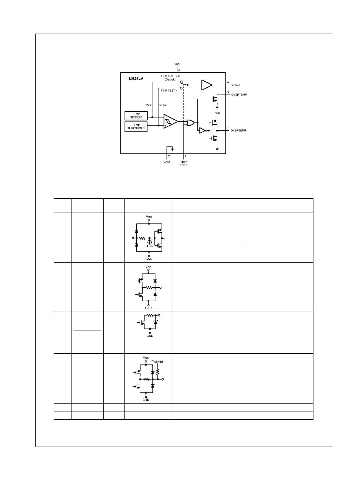
Block Diagram
20204703
Pin Descriptions
Pin
No.
Name Type Equivalent Circuit Description
1
TRIP
TEST
Digital
Input
TRIP TEST pin. Active High input.
If TRIP TEST = 0 (Default) then:
V
TEMP
= VTS, Temperature Sensor Output Voltage
If TRIP TEST = 1 then:
OVERTEMP and OVERTEMP outputs are asserted and
V
TEMP
= V
TRIP
, Temperature Trip Voltage.
This pin may be left open if not used.
5 OVERTEMP
Digital
Output
Over Temperature Switch output
Active High, Push-Pull
Asserted when the measured temperature exceeds the Trip
Point Temperature or if TRIP TEST = 1
This pin may be left open if not used.
3 OVERTEMP
Digital
Output
Over Temperature Switch output
Active Low, Open-drain (See Section 2.1 regarding required pullup resistor.)
Asserted when the measured temperature exceeds the Trip
Point Temperature or if TRIP TEST = 1
This pin may be left open if not used.
6
V
TEMP
Analog
Output
V
TEMP
Analog Voltage Output
If TRIP TEST = 0 then
V
TEMP
= VTS, Temperature Sensor Output Voltage
If TRIP TEST = 1 then
V
TEMP
= V
TRIP
, Temperature Trip Voltage
This pin may be left open if not used.
4
V
DD
Power
Positive Supply Voltage
2 GND Ground Power Supply Ground
www.national.com 2
LM26LV
Page 3
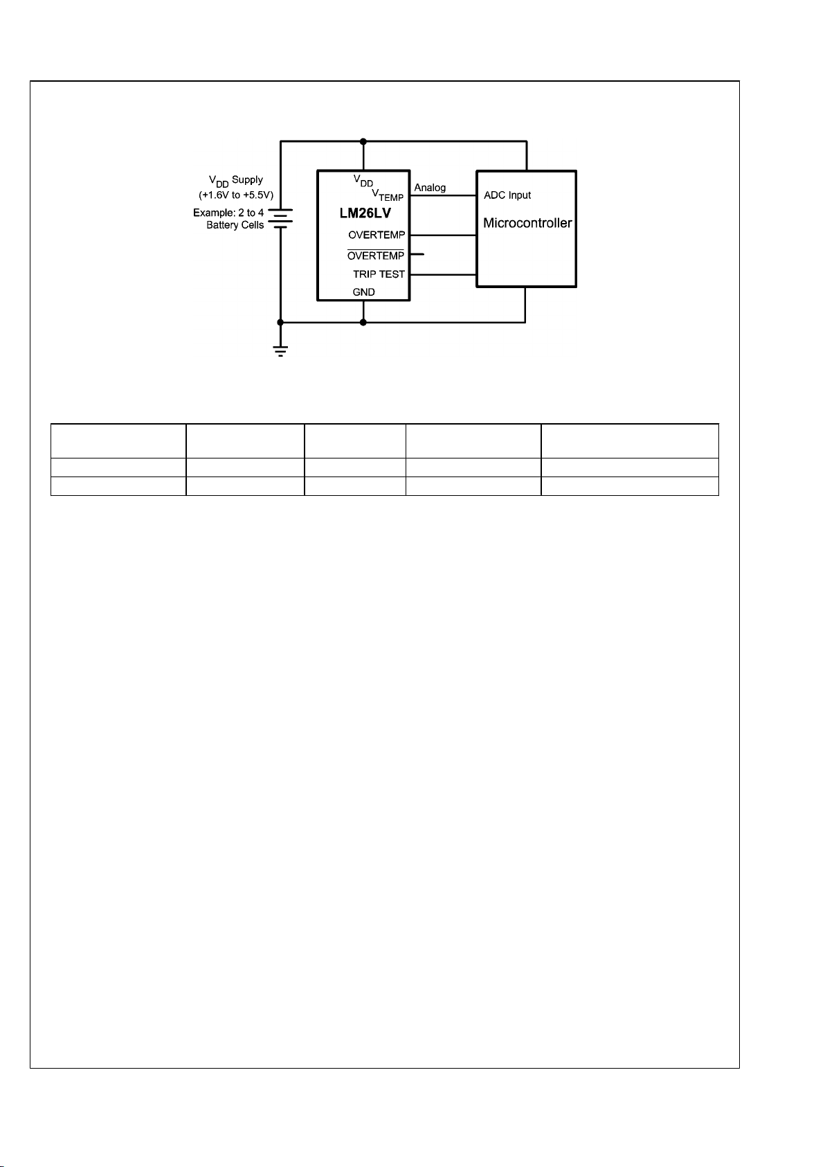
Typical Application
20204702
Ordering Information
Order Number
Temperature Trip
Point, °C
NS Package
Number
Top Mark Transport Media
LM26LVCISD-XPE 105°C SDB06A XPE 1000 Units on Tape and Reel
LM26LVCISDX-XPE 105°C SDB06A XPE 4500 Units on Tape and Reel
3 www.national.com
LM26LV
Page 4
Absolute Maximum Ratings (Note 1)
Supply Voltage −0.2V to +6.0V
Voltage at OVERTEMP pin −0.2V to +6.0V
Voltage at OVERTEMP and
V
TEMP
pins −0.2V to (VDD + 0.5V)
TRIP TEST Input Voltage −0.2V to (VDD + 0.5V)
Output Current, any output pin ±7 mA
Input Current at any pin (Note 2) 5 mA
Storage Temperature −65°C to +150°C
Maximum Junction Temperature
T
J(MAX)
+155°C
ESD Susceptibility (Note 3) :
Human Body Model 2500V
Machine Model 250V
Charged Device Model 1000V
Soldering process must comply with National's
Reflow Temperature Profile specifications. Refer to
www.national.com/packaging. (Note 4)
Operating Ratings (Note 1)
Specified Temperature Range:
T
MIN
≤ TA ≤ T
MAX
LM26LV
−50°C ≤ TA ≤ +150°C
Supply Voltage Range (VDD)
+1.6 V to +5.5 V
Thermal Resistance (θJA) (Note 5)
LLP-6 (Package SDB06A) 152 °C/W
Accuracy Characteristics
Trip Point Accuracy
Parameter Conditions
Limits
(Note 7)
Units
(Limit)
Trip Point Accuracy (Note 8) 0 − 150°C
VDD = 5.0 V
±2.2 °C (max)
V
TEMP
Analog Temperature Sensor Output Accuracy
There are four gains corresponding to each of the four Temperature Trip Point Ranges. Gain 1 is the sensor gain used for Temperature Trip Point 0 - 69°C. Likewise Gain 2 is for Trip Points 70 - 109 °C; Gain 3 for 110 - 129 °C; and Gain 4 for 130 - 150 °C.
These limits do not include DC load regulation. These stated accuracy limits are with reference to the values in the LM26LV
Conversion Table.
Parameter Conditions
Limits
(Note 7)
Units
(Limit)
V
TEMP
Temperature
Accuracy
(Note 8)
Gain 1: for Trip Point
Range 0 - 69°C
TA = 20°C to 40°C VDD = 1.6 to 5.5 V
±1.8
°C (max)
TA = 0°C to 70°C VDD = 1.6 to 5.5 V
±2.0
TA = 0°C to 90°C VDD = 1.6 to 5.5 V
±2.1
TA = 0°C to 120°C VDD = 1.6 to 5.5 V
±2.2
TA = 0°C to 150°C VDD = 1.6 to 5.5 V
±2.3
TA = −50°C to 0°C VDD = 1.7 to 5.5 V
±1.7
Gain 2: for Trip Point
Range 70 - 109°C
TA = 20°C to 40°C VDD = 1.8 to 5.5 V
±1.8
°C (max)
TA = 0°C to 70°C VDD = 1.9 to 5.5 V
±2.0
TA = 0°C to 90°C VDD = 1.9 to 5.5 V
±2.1
TA = 0°C to 120°C VDD = 1.9 to 5.5 V
±2.2
TA = 0°C to 150°C VDD = 1.9 to 5.5 V
±2.3
TA = −50°C to 0°C VDD = 2.3 to 5.5 V
±1.7
Gain 3: for Trip Point
Range 110 - 129°C
TA = 20°C to 40°C VDD = 2.3 to 5.5 V
±1.8
°C (max)
TA = 0°C to 70°C VDD = 2.5 to 5.5 V
±2.0
TA = 0°C to 90°C VDD = 2.5 to 5.5 V
±2.1
TA = 0°C to 120°C VDD = 2.5 to 5.5 V
±2.2
TA = 0°C to 150°C VDD = 2.5 to 5.5 V
±2.3
TA = −50°C to 0°C VDD = 3.0 to 5.5 V
±1.7
Gain 4: for Trip Point
Range 130 - 150°C
TA = 20°C to 40°C VDD = 2.7 to 5.5 V
±1.8
°C (max)
TA = 0°C to 70°C VDD = 3.0 to 5.5 V
±2.0
TA = 0°C to 90°C VDD = 3.0 to 5.5 V
±2.1
TA = 0°C to 120°C VDD = 3.0 to 5.5 V
±2.2
TA = 0°C to 150°C VDD = 3.0 to 5.5 V
±2.3
TA = −50°C to 0°C VDD = 3.6 to 5.5 V
±1.7
www.national.com 4
LM26LV
Page 5
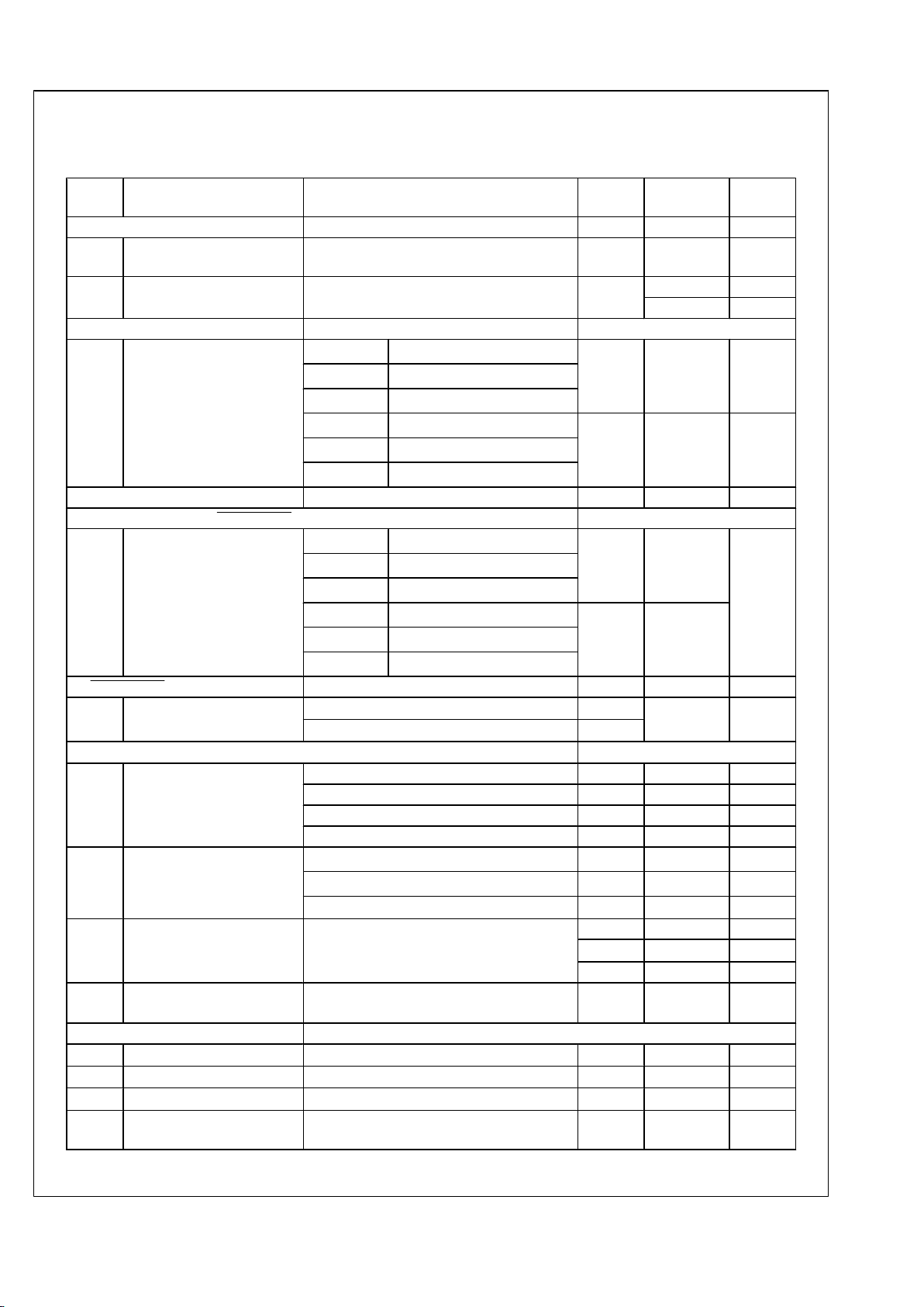
Electrical Characteristics
Unless otherwise noted, these specifications apply for +VDD = +1.6V to +5.5V. Boldface limits apply for TA = TJ = T
MIN
to
T
MAX
; all other limits TA = TJ = 25°C.
Symbol Parameter Conditions Typical
(Note 6)
Limits
(Note 7)
Units
(Limit)
GENERAL SPECIFICATIONS
I
S
Quiescent Power Supply
Current
8 16
μA (max)
Hysteresis
5
5.5 °C (max)
4.5 °C (Min)
OVERTEMP DIGITAL OUTPUT ACTIVE HIGH, PUSH-PULL
V
OH
Logic "1" Output Voltage
VDD ≥ 1.6V Source ≤ 340 μA
VDD − 0.2V
V (min)
VDD ≥ 2.0V Source ≤ 498 μA
VDD ≥ 3.3V Source ≤ 780 μA
VDD ≥ 1.6V Source ≤ 600 μA
VDD − 0.45V
V (min)
VDD ≥ 2.0V Source ≤ 980 μA
VDD ≥ 3.3V Source ≤ 1.6 mA
BOTH OVERTEMP and OVERTEMP DIGITAL OUTPUTS
V
OL
Logic "0" Output Voltage
VDD ≥ 1.6V Sink ≤ 385 μA
0.2
V (max)
VDD ≥ 2.0V Sink ≤ 500 μA
VDD ≥ 3.3V Sink ≤ 730 μA
VDD ≥ 1.6V Sink ≤ 690 μA
0.45
VDD ≥ 2.0V Sink ≤ 1.05 mA
VDD ≥ 3.3V Sink ≤ 1.62 mA
OVERTEMP DIGITAL OUTPUT ACTIVE LOW, OPEN DRAIN
I
OH
Logic "1" Output Leakage
Current (Note 12)
TA = 30 °C
0.001
1
μA (max)
TA = 150 °C
0.025
V
TEMP
ANALOG TEMPERATURE SENSOR OUTPUT
V
TEMP
Sensor Gain
Gain 1: If Trip Point = 0 - 69°C −5.1 mV/°C
Gain 2: If Trip Point = 70 - 109°C −7.7 mV/°C
Gain 3: If Trip Point = 110 - 129°C −10.3 mV/°C
Gain 4: If Trip Point = 130 - 150°C −12.8 mV/°C
V
TEMP
Load Regulation
(Note 10)
Source ≤ 90 μA, (VDD − V
TEMP
) ≥ 200 mV
−0.1 −1 mV (max)
Sink ≤ 100 μA, V
TEMP
≥ 260 mV
0.1 1 mV (max)
Source or Sink = 100 μA
1 Ohm
VDD Supply- to-V
TEMP
DC Line Regulation
(Note 13)
VDD = +1.6V to +5.5V
0.29 mV
74
μV/V
−82 dB
C
L
V
TEMP
Output Load
Capacitance
Without series resistor. See Section 4.2 1100
pF (max)
TRIP TEST DIGITAL INPUT
V
IH
Logic "1" Threshold Voltage
VDD− 0.5
V (min)
V
IL
Logic "0" Threshold Voltage
0.5 V (max)
I
IH
Logic "1" Input Current
1.5 2.5
μA (max)
I
IL
Logic "0" Input Current
(Note 12)
0.001 1
μA (max)
5 www.national.com
LM26LV
Page 6
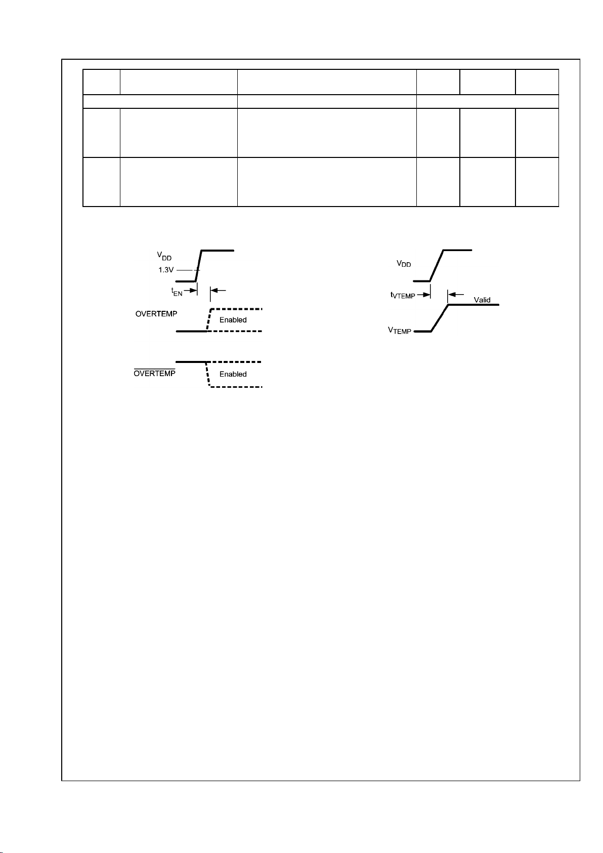
Symbol Parameter Conditions Typical
(Note 6)
Limits
(Note 7)
Units
(Limit)
TIMING
t
EN
Time from Power On to Digital
Output Enabled. See
definition below.
(Note 11).
1.1 10 ms (max)
t
V
TEMP
Time from Power On to
Analog Temperature Valid.
See definition below.
(Note 11)
0.9 10 ms (max)
Definitions of tEN and t
V
TEMP
20204750
20204751
Notes
Note 1: Absolute Maximum Ratings indicate limits beyond which damage to the device may occur. Operating Ratings indicate conditions for which the device is
functional, but do not guarantee specific performance limits. For guaranteed specifications and test conditions, see the Electrical Characteristics. The guaranteed
specifications apply only for the test conditions listed. Some performance characteristics may degrade when the device is not operated under the listed test
conditions.
Note 2: When the input voltage (VI) at any pin exceeds power supplies (VI < GND or VI > VDD), the current at that pin should be limited to 5 mA.
Note 3: The Human Body Model (HBM) is a 100 pF capacitor charged to the specified voltage then discharged through a 1.5 kΩ resistor into each pin. The
Machine Model (MM) is a 200 pF capacitor charged to the specified voltage then discharged directly into each pin. The Charged Device Model (CDM) is a specified
circuit characterizing an ESD event that occurs when a device acquires charge through some triboelectric (frictional) or electrostatic induction processes and then
abruptly touches a grounded object or surface.
Note 4: Reflow temperature profiles are different for lead-free and non-lead-free packages.
Note 5: The junction to ambient temperature resistance (θJA) is specified without a heat sink in still air.
Note 6: Typicals are at TJ = TA = 25°C and represent most likely parametric norm.
Note 7: Limits are guaranteed to National's AOQL (Average Outgoing Quality Level).
Note 8: Accuracy is defined as the error between the measured and reference output voltages, tabulated in the Conversion Table at the specified conditions of
supply gain setting, voltage, and temperature (expressed in °C). Accuracy limits include line regulation within the specified conditions. Accuracy limits do not
include load regulation; they assume no DC load.
Note 9: Changes in output due to self heating can be computed by multiplying the internal dissipation by the temperature resistance.
Note 10: Source currents are flowing out of the LM26LV. Sink currents are flowing into the LM26LV.
Note 11: Guaranteed by design.
Note 12: The 1 µA limit is based on a testing limitation and does not reflect the actual performance of the part. Expect to see a doubling of the current for every
15°C increase in temperature. For example, the 1 nA typical current at 25°C would increase to 16 nA at 85°C.
Note 13: Line regulation (DC) is calculated by subtracting the output voltage at the highest supply voltage from the output voltage at the lowest supply voltage.
The typical DC line regulation specification does not include the output voltage shift discussed in Section 4.3.
Note 14: The curves shown represent typical performance under worst-case conditions. Performance improves with larger overhead (VDD − V
TEMP
), larger VDD,
and lower temperatures.
Note 15: The curves shown represent typical performance under worst-case conditions. Performance improves with larger V
TEMP
, larger VDD and lower
temperatures.
www.national.com 6
LM26LV
Page 7
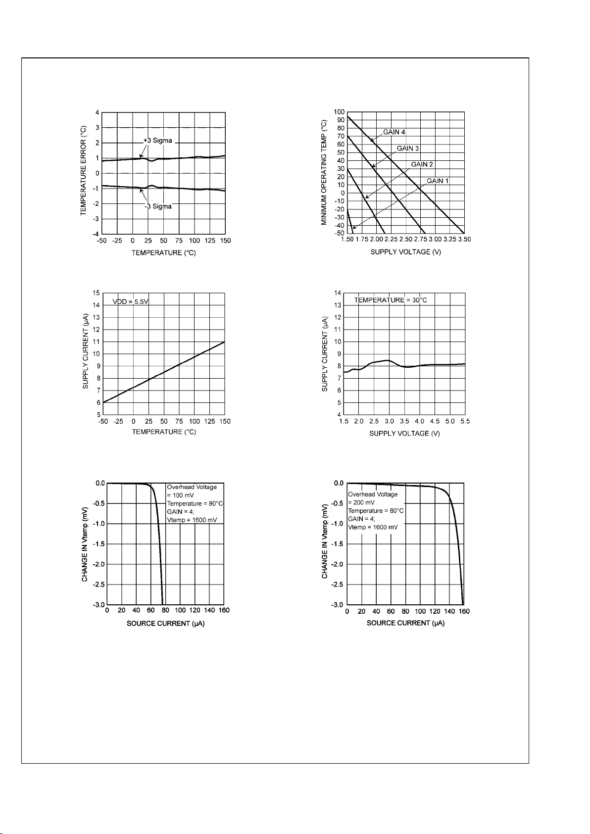
Typical Performance Characteristics
V
TEMP
Output Temperature Error vs. Temperature
20204707
Minimum Operating Temperature vs. Supply Voltage
20204706
Supply Current vs. Temperature
20204704
Supply Current vs. Supply Voltage
20204705
Load Regulation, 100 mV Overhead
T = 80°C Sourcing Current (Note 14)
20204740
Load Regulation, 200 mV Overhead
T = 80°C Sourcing Current (Note 14)
20204746
7 www.national.com
LM26LV
Page 8
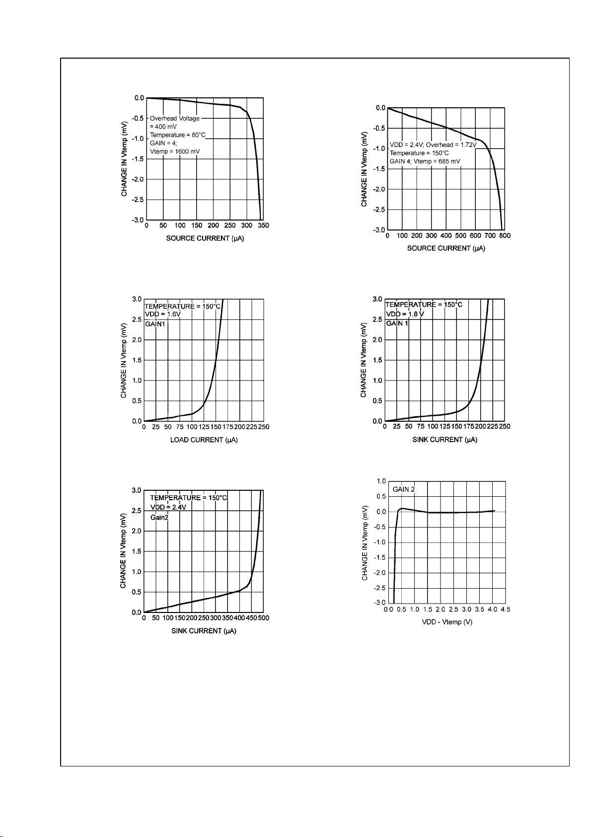
Load Regulation, 400 mV Overhead
T = 80°C Sourcing Current (Note 14)
20204747
Load Regulation, 1.72V Overhead
T = 150°C, VDD = 2.4V
Sourcing Current (Note 14)
20204748
Load Regulation, VDD = 1.6V
Sinking Current (Note 15)
20204741
Load Regulation, VDD = 1.8V
Sinking Current (Note 15)
20204744
Load Regulation, VDD = 2.4V
Sinking Current (Note 15)
20204745
Change in V
TEMP
vs. Overhead Voltage
20204742
www.national.com 8
LM26LV
Page 9
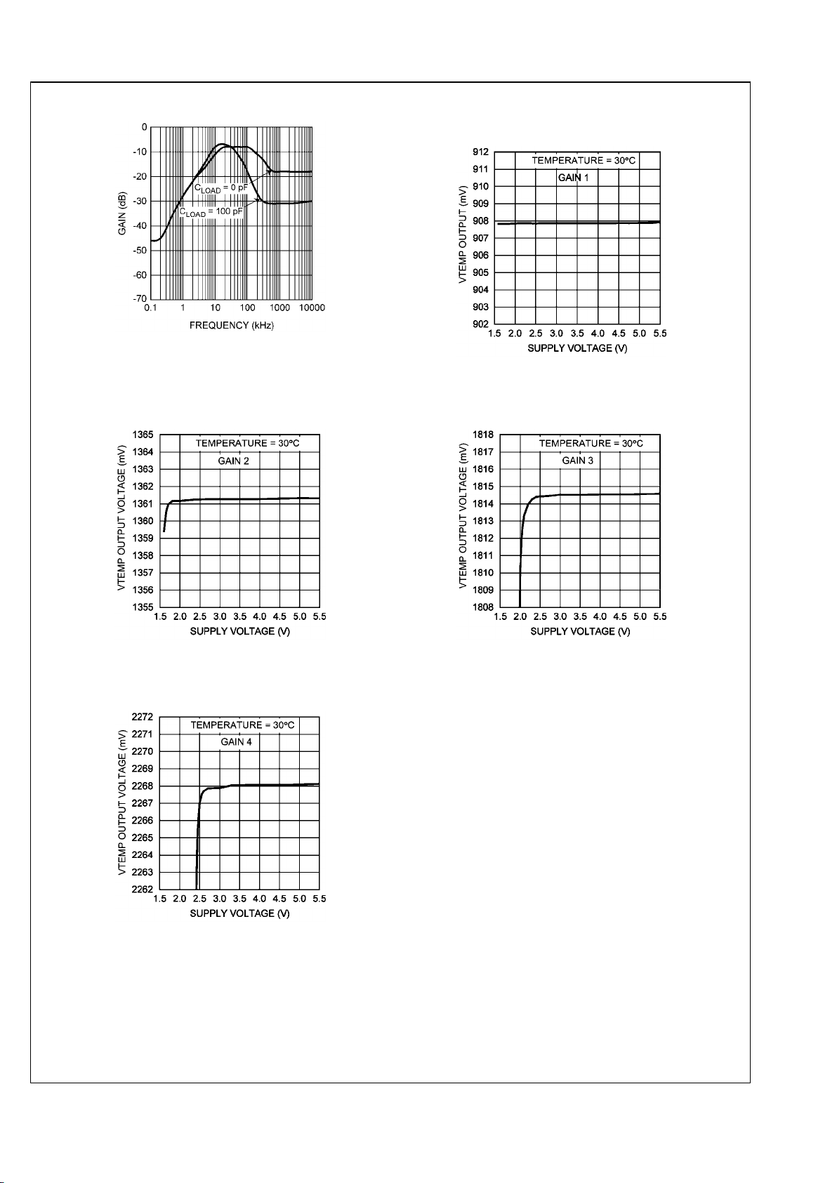
V
TEMP
Supply-Noise Gain vs. Frequency
20204743
V
TEMP
vs. Supply Voltage
Gain 1: For Trip Points
0 - 69°C
20204734
V
TEMP
vs. Supply Voltage
Gain 2: For Trip Points
70 - 109°C
20204735
V
TEMP
vs. Supply Voltage
Gain 3: For Trip Points
110 - 129°C
20204736
V
TEMP
vs. Supply Voltage
Gain 4: For Trip Points
130 - 150°C
20204737
9 www.national.com
LM26LV
Page 10
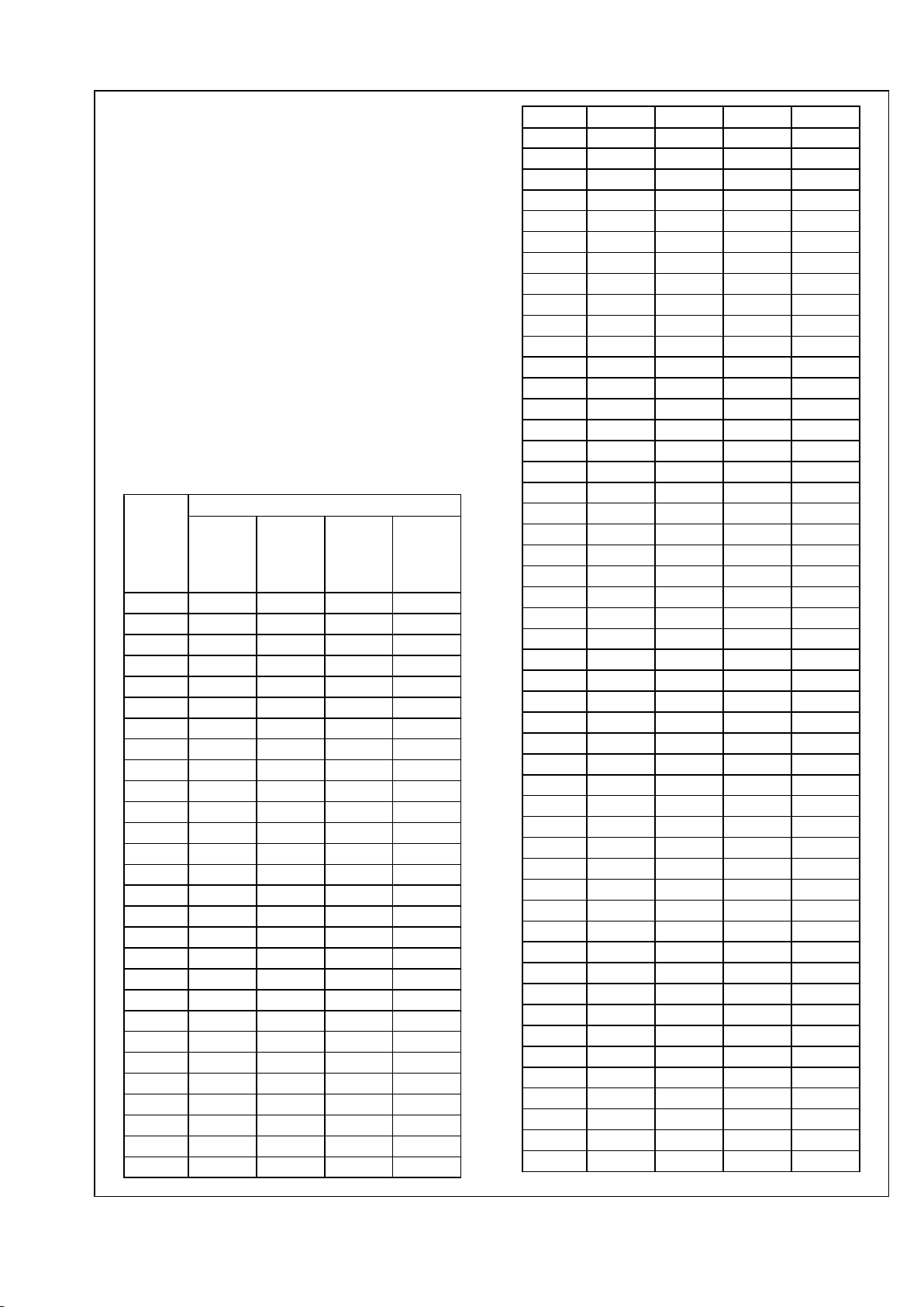
1.0 LM26LV V
TEMP
vs Die
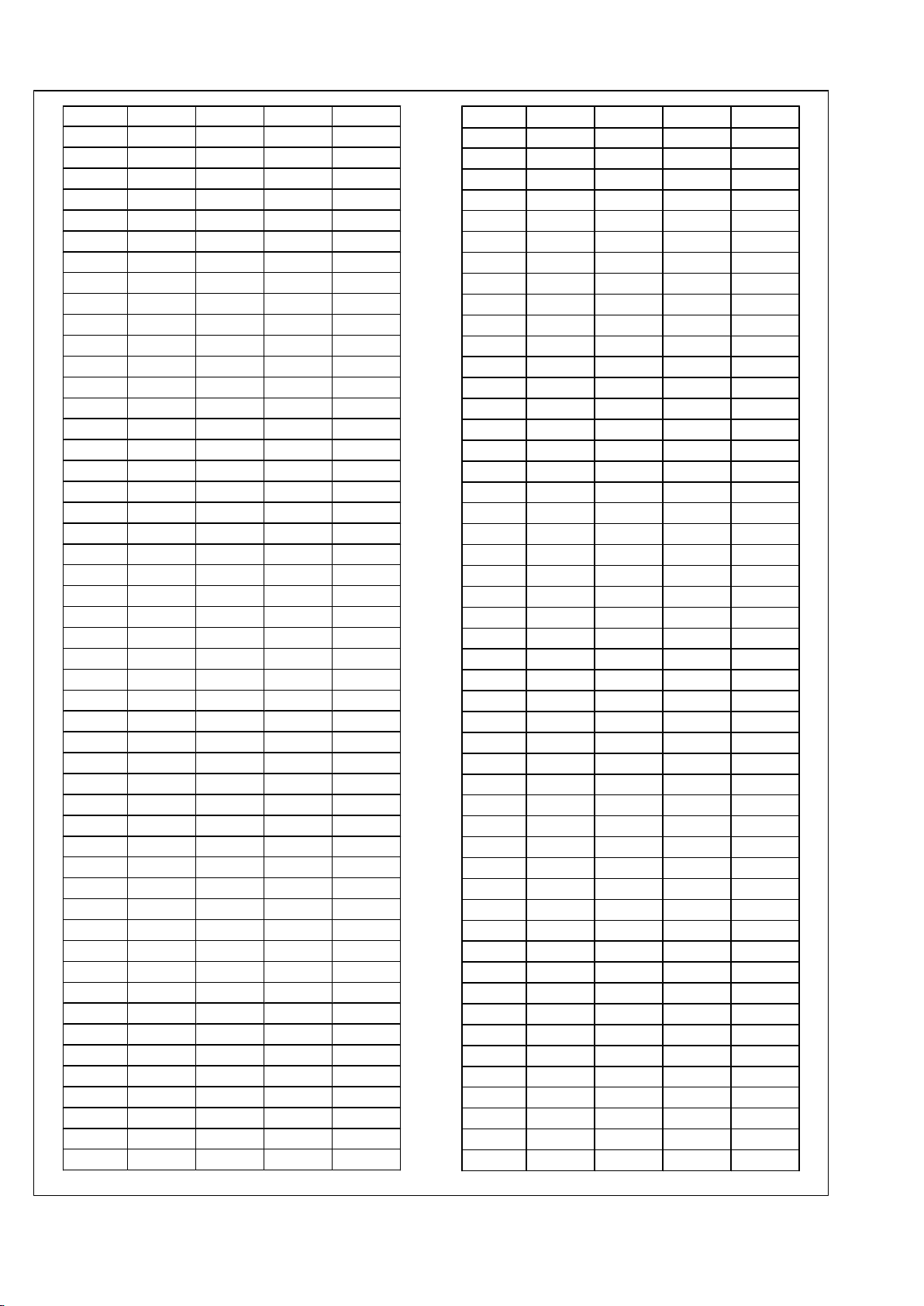
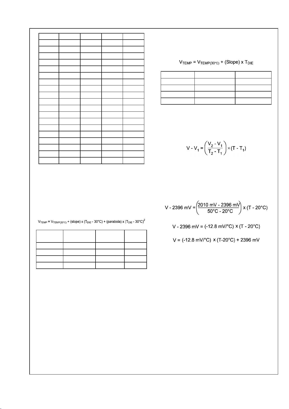
Temperature Conversion Table
The LM26LV has one out of four possible factory-set gains,
Gain 1 through Gain 4, depending on the range of the Temperature Trip Point. The V
TEMP
temperature sensor voltage,
in millivolts, at each discrete die temperature over the complete operating temperature range, and for each of the four
Temperature Trip Point ranges, is shown in the Conversion
Table below. This table is the reference from which the
LM26LV accuracy specifications (listed in the Electrical Characteristics section) are determined. This table can be used,
for example, in a host processor look-up table. See Section
1.1.1 for the parabolic equation used in the Conversion Table.
V
TEMP
Temperature Sensor Output Voltage vs Die
Temperature Conversion Table
The V
TEMP
temperature sensor output voltage, in mV, vs Die
Temperature, in °C, for each of the four gains corresponding
to each of the four Temperature Trip Point Ranges. Gain 1 is
the sensor gain used for Temperature Trip Point 0 - 69°C.
Likewise Gain 2 is for Trip Points 70 - 109 °C; Gain 3 for 110
- 129 °C; and Gain 4 for 130 - 150 °C. VDD = 5.0V. The values
in bold font are for the Trip Point range.
Die
Temp.,
°C
V
TEMP
, Analog Output Voltage, mV
Gain 1:
for
T
TRIP
=
0-69°C
Gain 2:
for
T
TRIP
=
70-109°C
Gain 3:
for
T
TRIP
=
110-129°C
Gain 4:
for
T
TRIP
=
130-150°C
−50 1312 1967 2623 3278
−49 1307 1960 2613 3266
−48 1302 1952 2603 3253
−47 1297 1945 2593 3241
−46 1292 1937 2583 3229
−45 1287 1930 2573 3216
−44 1282 1922 2563 3204
−43 1277 1915 2553 3191
−42 1272 1908 2543 3179
−41 1267 1900 2533 3166
−40 1262 1893 2523 3154
−39 1257 1885 2513 3141
−38 1252 1878 2503 3129
−37 1247 1870 2493 3116
−36 1242 1863 2483 3104
−35 1237 1855 2473 3091
−34 1232 1848 2463 3079
−33 1227 1840 2453 3066
−32 1222 1833 2443 3054
−31 1217 1825 2433 3041
−30 1212 1818 2423 3029
−29 1207 1810 2413 3016
−28 1202 1803 2403 3004
−27 1197 1795 2393 2991
−26 1192 1788 2383 2979
−25 1187 1780 2373 2966
−24 1182 1773 2363 2954
−23 1177 1765 2353 2941
−22 1172 1757 2343 2929
−21 1167 1750 2333 2916
−20 1162 1742 2323 2903
−19 1157 1735 2313 2891
−18 1152 1727 2303 2878
−17 1147 1720 2293 2866
−16 1142 1712 2283 2853
−15 1137 1705 2272 2841
−14 1132 1697 2262 2828
−13 1127 1690 2252 2815
−12 1122 1682 2242 2803
−11 1116 1674 2232 2790
−10 1111 1667 2222 2777
−9 1106 1659 2212 2765
−8 1101 1652 2202 2752
−7 1096 1644 2192 2740
−6 1091 1637 2182 2727
−5 1086 1629 2171 2714
−4 1081 1621 2161 2702
−3 1076 1614 2151 2689
−2 1071 1606 2141 2676
−1 1066 1599 2131 2664
0 1061 1591 2121 2651
1 1056 1583 2111 2638
2 1051 1576 2101 2626
3 1046 1568 2090 2613
4 1041 1561 2080 2600
5 1035 1553 2070 2587
6 1030 1545 2060 2575
7 1025 1538 2050 2562
8 1020 1530 2040 2549
9 1015 1522 2029 2537
10 1010 1515 2019 2524
11 1005 1507 2009 2511
12 1000 1499 1999 2498
13 995 1492 1989 2486
14 990 1484 1978 2473
15 985 1477 1968 2460
16 980 1469 1958 2447
17 974 1461 1948 2435
18 969 1454 1938 2422
19 964 1446 1927 2409
20 959 1438 1917 2396
21 954 1431 1907 2383
22 949 1423 1897 2371
23 944 1415 1886 2358
24 939 1407 1876 2345
25 934 1400 1866 2332
26 928 1392 1856 2319
27 923 1384 1845 2307
28 918 1377 1835 2294
www.national.com 10
LM26LV
Page 11
29 913 1369 1825 2281
30 908 1361 1815 2268
31 903 1354 1804 2255
32 898 1346 1794 2242
33 892 1338 1784 2230
34 887 1331 1774 2217
35 882 1323 1763 2204
36 877 1315 1753 2191
37 872 1307 1743 2178
38 867 1300 1732 2165
39 862 1292 1722 2152
40 856 1284 1712 2139
41 851 1276 1701 2127
42 846 1269 1691 2114
43 841 1261 1681 2101
44 836 1253 1670 2088
45 831 1245 1660 2075
46 825 1238 1650 2062
47 820 1230 1639 2049
48 815 1222 1629 2036
49 810 1214 1619 2023
50 805 1207 1608 2010
51 800 1199 1598 1997
52 794 1191 1588 1984
53 789 1183 1577 1971
54 784 1176 1567 1958
55 779 1168 1557 1946
56 774 1160 1546 1933
57 769 1152 1536 1920
58 763 1144 1525 1907
59 758 1137 1515 1894
60 753 1129 1505 1881
61 748 1121 1494 1868
62 743 1113 1484 1855
63 737 1105 1473 1842
64 732 1098 1463 1829
65 727 1090 1453 1816
66 722 1082 1442 1803
67 717 1074 1432 1790
68 711 1066 1421 1776
69 706 1059 1411 1763
70 701 1051 1400 1750
71 696 1043 1390 1737
72 690 1035 1380 1724
73 685 1027 1369 1711
74 680 1019 1359 1698
75 675 1012 1348 1685
76 670 1004 1338 1672
77 664 996 1327 1659
78 659 988 1317 1646
79 654 980 1306 1633
80 649 972 1296 1620
81 643 964 1285 1607
82 638 957 1275 1593
83 633 949 1264 1580
84 628 941 1254 1567
85 622 933 1243 1554
86 617 925 1233 1541
87 612 917 1222 1528
88 607 909 1212 1515
89 601 901 1201 1501
90 596 894 1191 1488
91 591 886 1180 1475
92 586 878 1170 1462
93 580 870 1159 1449
94 575 862 1149 1436
95 570 854 1138 1422
96 564 846 1128 1409
97 559 838 1117 1396
98 554 830 1106 1383
99 549 822 1096 1370
100 543 814 1085 1357
101 538 807 1075 1343
102 533 799 1064 1330
103 527 791 1054 1317
104 522 783 1043 1304
105 517 775 1032 1290
106 512 767 1022 1277
107 506 759 1011 1264
108 501 751 1001 1251
109 496 743 990 1237
110 490 735 979 1224
111 485 727 969 1211
112 480 719 958 1198
113 474 711 948 1184
114 469 703 937 1171
115 464 695 926 1158
116 459 687 916 1145
117 453 679 905 1131
118 448 671 894 1118
119 443 663 884 1105
120 437 655 873 1091
121 432 647 862 1078
122 427 639 852 1065
123 421 631 841 1051
124 416 623 831 1038
125 411 615 820 1025
126 405 607 809 1011
127 400 599 798 998
128 395 591 788 985
129 389 583 777 971
130 384 575 766 958
11 www.national.com
LM26LV
Page 12
131 379 567 756 945
132 373 559 745 931
133 368 551 734 918
134 362 543 724 904
135 357 535 713 891
136 352 527 702 878
137 346 519 691 864
138 341 511 681 851
139 336 503 670 837
140 330 495 659 824
141 325 487 649 811
142 320 479 638 797
143 314 471 627 784
144 309 463 616 770
145 303 455 606 757
146 298 447 595 743
147 293 438 584 730
148 287 430 573 716
149 282 422 562 703
150 277 414 552 690
1.1 V
TEMP
vs DIE TEMPERATURE APPROXIMATIONS
The LM26LV's V
TEMP
analog temperature output is very lin-
ear. The Conversion Table above and the equation in Section
1.1.1 represent the most accurate typical performance of the
V
TEMP
voltage output vs Temperature.
1.1.1 The Second-Order Equation (Parabolic)
The data from the Conversion Table, or the equation below,
when plotted, has an umbrella-shaped parabolic curve.
Sensor Gain
V
TEMP(30°C)
, mV
Slope, mV/°C
Parabola,
mV/°C
2
GAIN 1 907.87 -5.1321 -0.001076
GAIN 2 1361.35 -7.7011 -0.001596
GAIN 3 1814.62 -10.2703 -0.002117
GAIN 4 2268.14 -12.8384 -0.002639
1.1.2 The First-Order Approximation (Linear)
For a quicker approximation, although less accurate than the
second-order, over the full operating temperature range the
linear formula below can be used. Using this formula, with the
offset and slope in the following table, the best-fit V
TEMP
vs
Die Temperature performance can be calculated with an approximation error less than 18 mV.
Sensor Gain
V
TEMP(30°C)
, mV
Slope, mV/°C
GAIN 1 1059.9 -5.1751
GAIN 2 1589.9 -7.765
GAIN 3 2119.0 -10.355
GAIN 4 2648.6 -12.944
1.1.3 First-Order Approximation (Linear) over Small
Temperature Range
For a linear approximation, a line can easily be calculated
over the desired temperature range from the Conversion Table using the two-point equation:
Where V is in mV, T is in °C, T1 and V1 are the coordinates of
the lowest temperature, T2 and V2 are the coordinates of the
highest temperature.
For example, if we want to determine the equation of a line
with Gain 4, over a temperature range of 20°C to 50°C, we
would proceed as follows:
Using this method of linear approximation, the transfer function can be approximated for one or more temperature ranges
of interest.
www.national.com 12
LM26LV
Page 13
2.0 OVERTEMP and OVERTEMP
Digital Outputs
The OVERTEMP Active High, Push-Pull Output and the
OVERTEMP
Active Low, Open-Drain Output both assert at
the same time whenever the Die Temperature reaches the
factory preset Temperature Trip Point. They also assert simultaneously whenever the TRIP TEST pin is set high. Both
outputs de-assert when the die temperature goes below the
Temperature Trip Point - Hysteresis. These two types of digital outputs enable the user the flexibility to choose the type
of output that is most suitable for his design.
Either the OVERTEMP or the OVERTEMP Digital Output pins
can be left open if not used.
2.1 OVERTEMP
OPEN-DRAIN DIGITAL OUTPUT
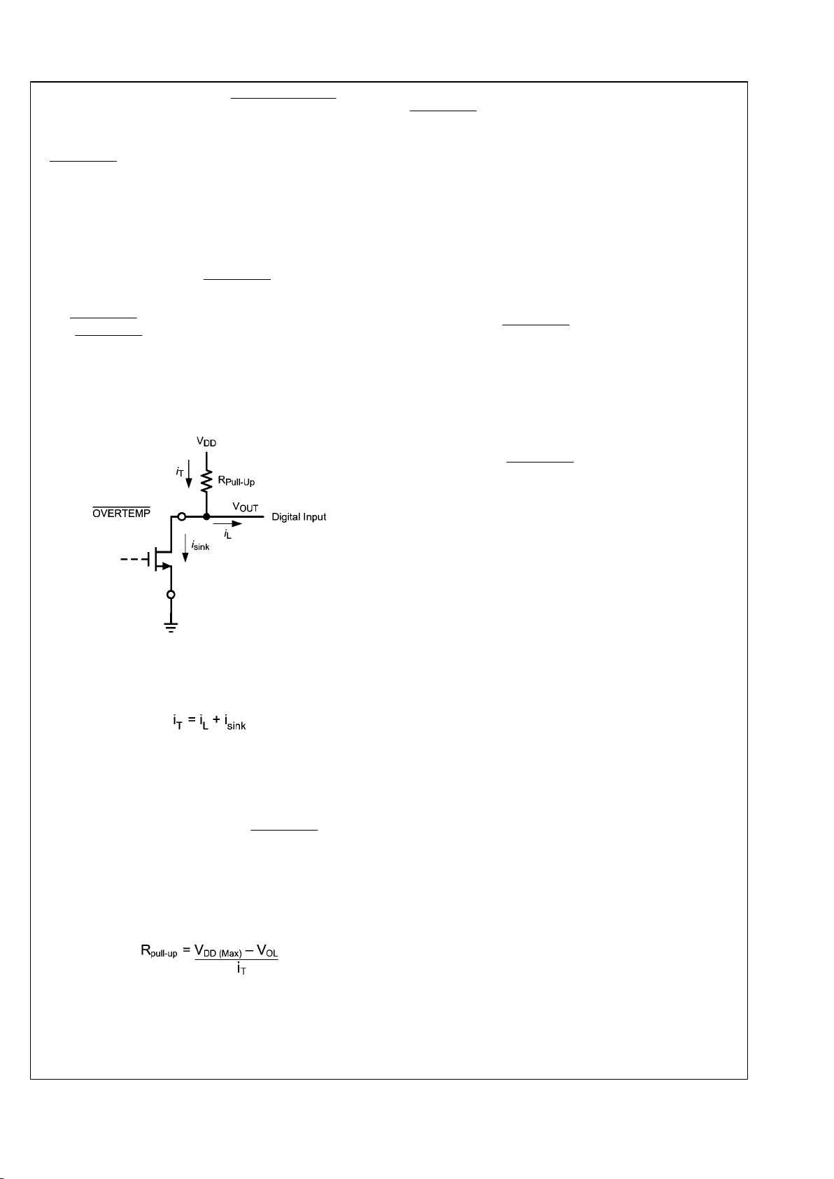
The OVERTEMP
Active Low, Open-Drain Digital Output, if
used, requires a pull-up resistor between this pin and VDD.
The following section shows how to determine the pull-up resistor value.
Determining the Pull-up Resistor Value
20204752
The Pull-up resistor value is calculated at the condition of
maximum total current, iT, through the resistor. The total current is:
where,
i
T
iT is the maximum total current through the Pull-up
Resistor at VOL.
i
L
iL is the load current, which is very low for typical
digital inputs.
V
OUT
V
OUT
is the Voltage at the OVERTEMP pin. Use
VOL for calculating the Pull-up resistor.
V
DD(Max)
V
DD(Max)
is the maximum power supply voltage to be
used in the customer's system.
The pull-up resistor maximum value can be found by using
the following formula:
EXAMPLE CALCULATION
Suppose we have, for our example, a VDD of 3.3 V ± 0.3V, a
CMOS digital input as a load, a VOL of 0.2 V.
(1) We see that for VOL of 0.2 V the electrical specification for
OVERTEMP shows a maximim i
sink
of 385 µA.
(2) Let iL= 1 µA, then iT is about 386 µA max. If we select
35 µA as the current limit then iT for the calculation becomes
35 µA
(3) We notice that V
DD(Max)
is 3.3V + 0.3V = 3.6V and then
calculate the pull-up resistor as
R
Pull-up
= (3.6 − 0.2)/35 µA = 97k
(4) Based on this calculated value, we select the closest resistor value in the tolerance family we are using.
In our example, if we are using 5% resistor values, then the
next closest value is 100 kΩ.
2.2 NOISE IMMUNITY
The LM26LV is virtually immune from false triggers on the
OVERTEMP and OVERTEMP digital outputs due to noise on
the power supply. Test have been conducted showing that,
with the die temperature within 0.5°C of the temperature trip
point, and the severe test of a 3 Vpp square wave "noise"
signal injected on the VDD line, over the VDD range of 2V to
5V, there were no false triggers.
3.0 TRIP TEST Digital Input
The TRIP TEST pin simply provides a means to test the
OVERTEMP and OVERTEMP digital outputs electronically
by causing them to assert, at any operating temperature, as
a result of forcing the TRIP TEST pin high.
When the TRIP TEST pin is pulled high the V
TEMP
pin will be
at the V
TRIP
voltage.
If not used, the TRIP TEST pin may either be left open or
grounded.
4.0 V
TEMP
Analog Temperature
Sensor Output
The V
TEMP
push-pull output provides the ability to sink and
source significant current. This is beneficial when, for example, driving dynamic loads like an input stage on an analogto-digital converter (ADC). In these applications the source
current is required to quickly charge the input capacitor of the
ADC. See the Applications Circuits section for more discussion of this topic. The LM26LV is ideal for this and other
applications which require strong source or sink current.
4.1 NOISE CONSIDERATIONS
The LM26LV's supply-noise gain (the ratio of the AC signal
on V
TEMP
to the AC signal on VDD) was measured during
bench tests. It's typical attenuation is shown in the Typical
Performance Characteristics section. A load capacitor on the
output can help to filter noise.
For operation in very noisy environments, some bypass capacitance should be present on the supply within approximately 2 inches of the LM26LV.
4.2 CAPACITIVE LOADS
The V
TEMP
Output handles capacitive loading well. In an extremely noisy environment, or when driving a switched sampling input on an ADC, it may be necessary to add some
filtering to minimize noise coupling. Without any precautions,
the V
TEMP
can drive a capacitive load less than or equal to
1100 pF as shown in Figure 1. For capacitive loads greater
than 1100 pF, a series resistor is required on the output, as
shown in Figure 2, to maintain stable conditions.
13 www.national.com
LM26LV
Page 14
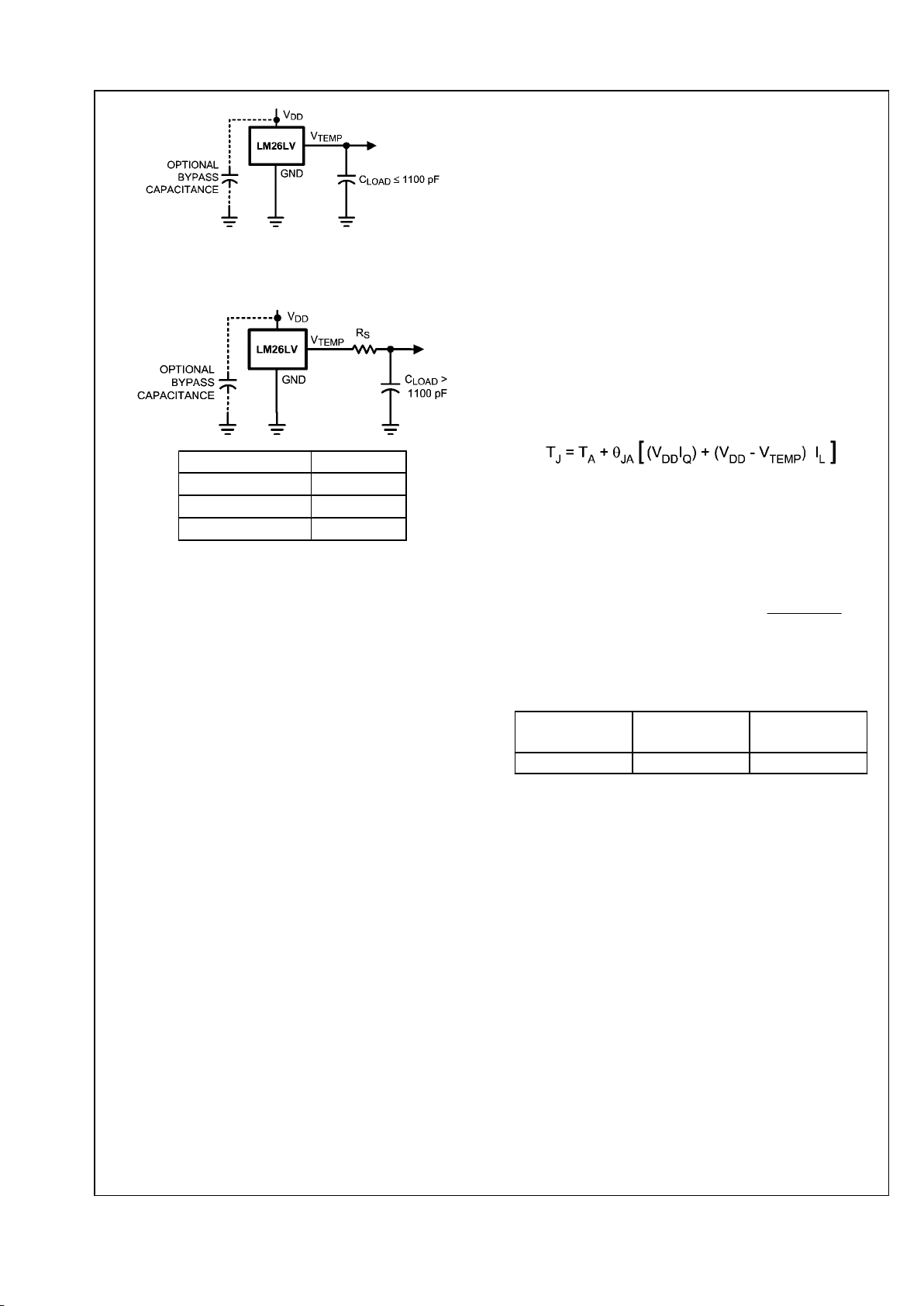
20204715
FIGURE 1. LM26LV No Decoupling Required for
Capacitive Loads Less than 1100 pF.
20204733
C
LOAD
R
S
1.1 nF to 99 nF
3 kΩ
100 nF to 999 nF
1.5 kΩ
1 μF
800 Ω
FIGURE 2. LM26LV with series resistor for capacitive
loading greater than 1100 pF.
4.3 VOLTAGE SHIFT
The LM26LV is very linear over temperature and supply voltage range. Due to the intrinsic behavior of an NMOS/PMOS
rail-to-rail buffer, a slight shift in the output can occur when
the supply voltage is ramped over the operating range of the
device. The location of the shift is determined by the relative
levels of VDD and V
TEMP
. The shift typically occurs when
VDD − V
TEMP
= 1.0V.
This slight shift (a few millivolts) takes place over a wide
change (approximately 200 mV) in VDD or V
TEMP
. Since the
shift takes place over a wide temperature change of 5°C to
20°C, V
TEMP
is always monotonic. The accuracy specifications in the Electrical Characteristics table already includes
this possible shift.
5.0 Mounting and Temperature
Conductivity
The LM26LV can be applied easily in the same way as other
integrated-circuit temperature sensors. It can be glued or cemented to a surface.
To ensure good temperature conductivity, the backside of the
LM26LV die is directly attached to the GND pin (Pin 2). The
temperatures of the lands and traces to the other leads of the
LM26LV will also affect the temperature reading.
Alternatively, the LM26LV can be mounted inside a sealedend metal tube, and can then be dipped into a bath or screwed
into a threaded hole in a tank. As with any IC, the LM26LV
and accompanying wiring and circuits must be kept insulated
and dry, to avoid leakage and corrosion. This is especially true
if the circuit may operate at cold temperatures where condensation can occur. If moisture creates a short circuit from
the V
TEMP
output to ground or VDD, the V
TEMP
output from the
LM26LV will not be correct. Printed-circuit coatings are often
used to ensure that moisture cannot corrode the leads or circuit traces.
The thermal resistance junction-to-ambient (θJA) is the parameter used to calculate the rise of a device junction temperature due to its power dissipation. The equation used to
calculate the rise in the LM26LV's die temperature is
where TA is the ambient temperature, IQ is the quiescent current, IL is the load current on the output, and VO is the output
voltage. For example, in an application where TA = 30 °C,
VDD = 5 V, IDD = 9 μA, Gain 4, V
TEMP
= 2231 mV, and
IL = 2 μA, the junction temperature would be 30.021 °C, showing a self-heating error of only 0.021°C. Since the LM26LV's
junction temperature is the actual temperature being measured, care should be taken to minimize the load current that
the V
TEMP
output is required to drive. If The OVERTEMP output is used with a 100 k pull-up resistor, and this output is
asserted (low), then for this example the additional contribution is [(152° C/W)x(5V)2/100k] = 0.038°C for a total selfheating error of 0.059°C. Figure 3 shows the thermal
resistance of the LM26LV.
Device Number
NS Package
Number
Thermal
Resistance (θJA)
LM26LVCISD SDB06A 152° C/W
FIGURE 3. LM26LV Thermal Resistance
www.national.com 14
LM26LV
Page 15
6.0 Applications Circuits
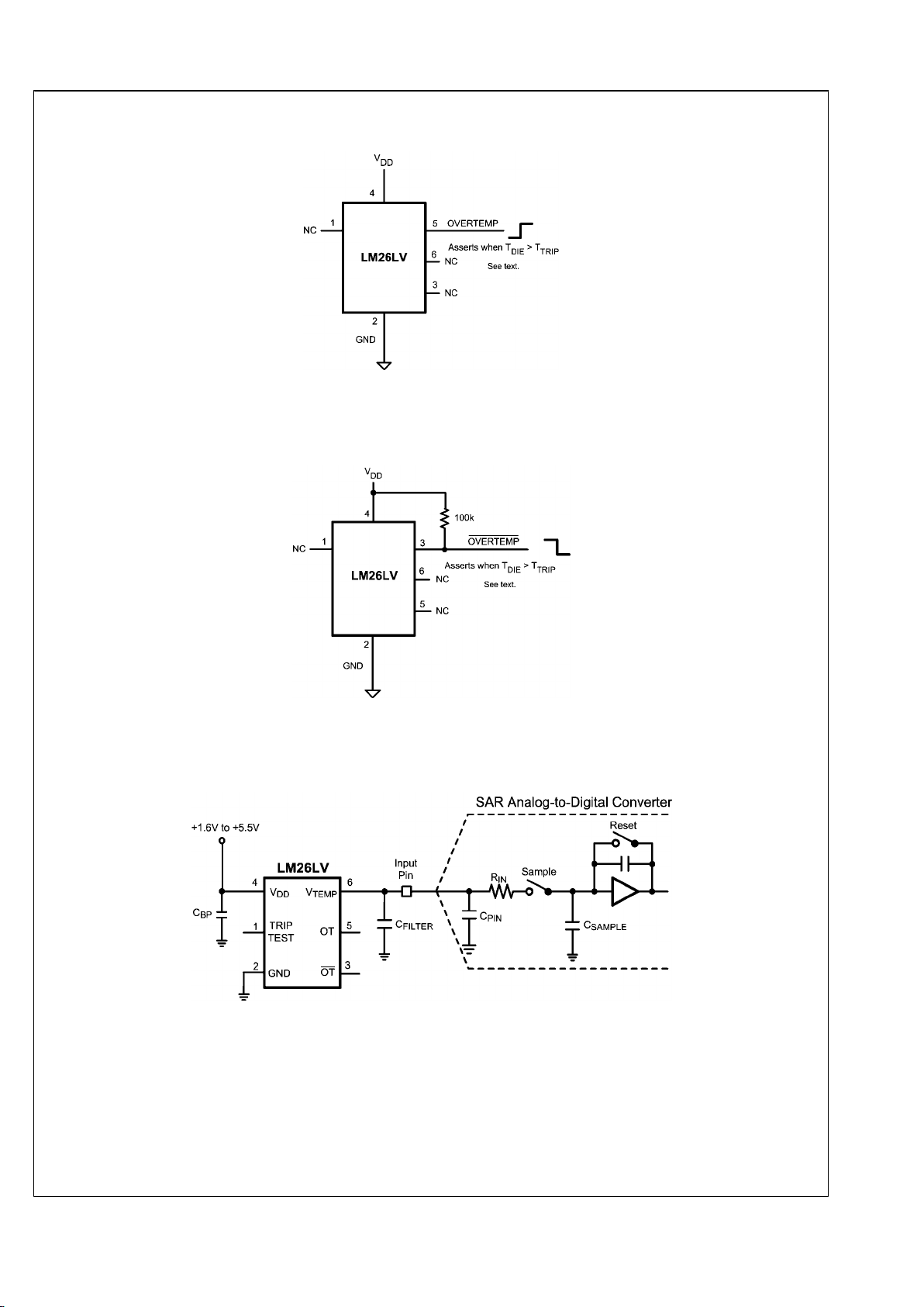
20204761
FIGURE 4. Temperature Switch Using Push-Pull Output
20204762
FIGURE 5. Temperature Switch Using Open-Drain Output
20204728
Most CMOS ADCs found in microcontrollers and ASICs have a sampled data comparator input structure. When the ADC charges
the sampling cap, it requires instantaneous charge from the output of the analog source such as the LM26LV temperature sensor
and many op amps. This requirement is easily accommodated by the addition of a capacitor (C
FILTER
). The size of C
FILTER
depends
on the size of the sampling capacitor and the sampling frequency. Since not all ADCs have identical input stages, the charge
requirements will vary. This general ADC application is shown as an example only.
FIGURE 6. Suggested Connection to a Sampling Analog-to-Digital Converter Input Stage
15 www.national.com
LM26LV
Page 16
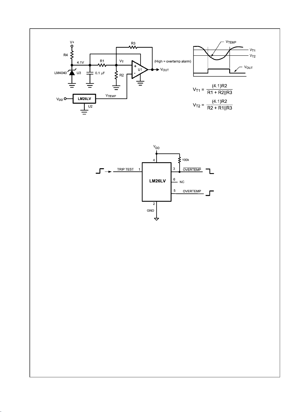
20204718
FIGURE 7. Celsius Temperature Switch
20204760
FIGURE 8. TRIP TEST Digital Output Test Circuit
www.national.com 16
LM26LV
Page 17
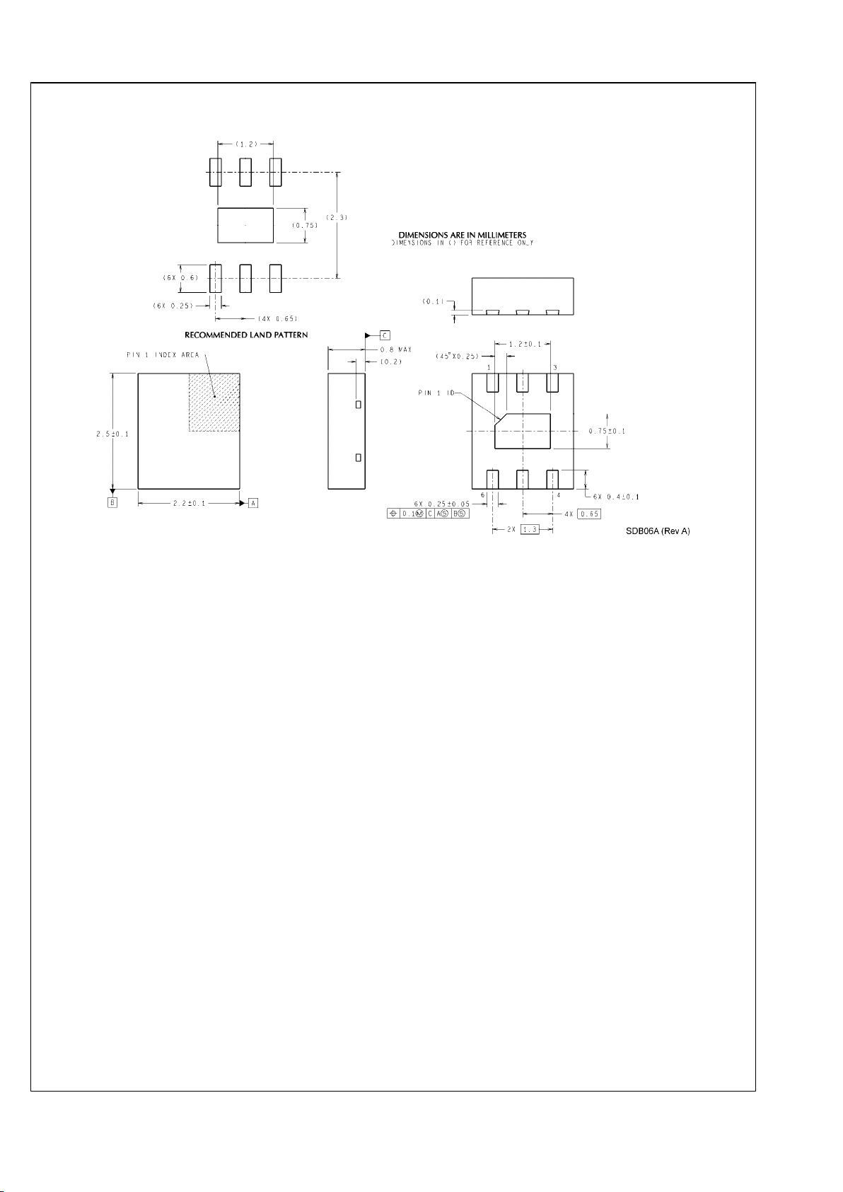
Physical Dimensions inches (millimeters) unless otherwise noted
6-Lead LLP-6 Package
Order Number LM26LVCISD, LM26LVCISDX
NS Package Number SDB06A
17 www.national.com
LM26LV
Page 18
Notes
LM26LV 1.6 V, LLP-6 Factory Preset Temperature Switch and Temperature Sensor
THE CONTENTS OF THIS DOCUMENT ARE PROVIDED IN CONNECTION WITH NATIONAL SEMICONDUCTOR CORPORATION
(“NATIONAL”) PRODUCTS. NATIONAL MAKES NO REPRESENTATIONS OR WARRANTIES WITH RESPECT TO THE ACCURACY
OR COMPLETENESS OF THE CONTENTS OF THIS PUBLICATION AND RESERVES THE RIGHT TO MAKE CHANGES TO
SPECIFICATIONS AND PRODUCT DESCRIPTIONS AT ANY TIME WITHOUT NOTICE. NO LICENSE, WHETHER EXPRESS,
IMPLIED, ARISING BY ESTOPPEL OR OTHERWISE, TO ANY INTELLECTUAL PROPERTY RIGHTS IS GRANTED BY THIS
DOCUMENT.
TESTING AND OTHER QUALITY CONTROLS ARE USED TO THE EXTENT NATIONAL DEEMS NECESSARY TO SUPPORT
NATIONAL’S PRODUCT WARRANTY. EXCEPT WHERE MANDATED BY GOVERNMENT REQUIREMENTS, TESTING OF ALL
PARAMETERS OF EACH PRODUCT IS NOT NECESSARILY PERFORMED. NATIONAL ASSUMES NO LIABILITY FOR
APPLICATIONS ASSISTANCE OR BUYER PRODUCT DESIGN. BUYERS ARE RESPONSIBLE FOR THEIR PRODUCTS AND
APPLICATIONS USING NATIONAL COMPONENTS. PRIOR TO USING OR DISTRIBUTING ANY PRODUCTS THAT INCLUDE
NATIONAL COMPONENTS, BUYERS SHOULD PROVIDE ADEQUATE DESIGN, TESTING AND OPERATING SAFEGUARDS.
EXCEPT AS PROVIDED IN NATIONAL’S TERMS AND CONDITIONS OF SALE FOR SUCH PRODUCTS, NATIONAL ASSUMES NO
LIABILITY WHATSOEVER, AND NATIONAL DISCLAIMS ANY EXPRESS OR IMPLIED WARRANTY RELATING TO THE SALE
AND/OR USE OF NATIONAL PRODUCTS INCLUDING LIABILITY OR WARRANTIES RELATING TO FITNESS FOR A PARTICULAR
PURPOSE, MERCHANTABILITY, OR INFRINGEMENT OF ANY PATENT, COPYRIGHT OR OTHER INTELLECTUAL PROPERTY
RIGHT.
LIFE SUPPORT POLICY
NATIONAL’S PRODUCTS ARE NOT AUTHORIZED FOR USE AS CRITICAL COMPONENTS IN LIFE SUPPORT DEVICES OR
SYSTEMS WITHOUT THE EXPRESS PRIOR WRITTEN APPROVAL OF THE CHIEF EXECUTIVE OFFICER AND GENERAL
COUNSEL OF NATIONAL SEMICONDUCTOR CORPORATION. As used herein:
Life support devices or systems are devices which (a) are intended for surgical implant into the body, or (b) support or sustain life and
whose failure to perform when properly used in accordance with instructions for use provided in the labeling can be reasonably expected
to result in a significant injury to the user. A critical component is any component in a life support device or system whose failure to perform
can be reasonably expected to cause the failure of the life support device or system or to affect its safety or effectiveness.
National Semiconductor and the National Semiconductor logo are registered trademarks of National Semiconductor Corporation. All other
brand or product names may be trademarks or registered trademarks of their respective holders.
Copyright© 2007 National Semiconductor Corporation
For the most current product information visit us at www.national.com
National Semiconductor
Americas Customer
Support Center
Email:
[email protected]
Tel: 1-800-272-9959
National Semiconductor Europe
Customer Support Center
Fax: +49 (0) 180-530-85-86
Email: [email protected]
Deutsch Tel: +49 (0) 69 9508 6208
English Tel: +49 (0) 870 24 0 2171
Français Tel: +33 (0) 1 41 91 8790
National Semiconductor Asia
Pacific Customer Support Center
Email: [email protected]
National Semiconductor Japan
Customer Support Center
Fax: 81-3-5639-7507
Email: [email protected]
Tel: 81-3-5639-7560
www.national.com
 Loading...