

查询10MV5600AX供应商
LM2727/LM2737
N-Channel FET Synchronous Buck Regulator Controller
for Low Output Voltages
LM2727/LM2737 N-Channel FET Synchronous Buck Regulator Controller for Low Output Voltages
June 2003
General Description
The LM2727 and LM2737 are high-speed, synchronous,
switching regulator controllers. They are intended to control
currents of 0.7A to 20A with up to 95% conversion efficiencies. The LM2727 employs output over-voltage and undervoltage latch-off. For applications where latch-off is not desired, the LM2737 can be used. Power up and down
sequencing is achieved with the power-good flag, adjustable
soft-start and output enable features. The LM2737 and
LM2737 operate from a low-current 5V bias and can convert
from a 2.2V to 16V power rail. Both parts utilize a fixedfrequency, voltage-mode, PWM control architecture and the
switching frequency is adjustable from 50kHz to 2MHz by
adjusting the value of an external resistor. Current limit is
achieved by monitoring the voltage drop across the onresistance of the low-side MOSFET, which enhances low
duty-cycle operation. The wide range of operating frequencies gives the power supply designer the flexibility to finetune component size, cost, noise and efficiency. The adaptive, non-overlapping MOSFET gate-drivers and high-side
bootstrap structure helps to further maximize efficiency. The
high-side power FET drain voltage can be from 2.2V to 16V
and the output voltage is adjustable down to 0.6V.
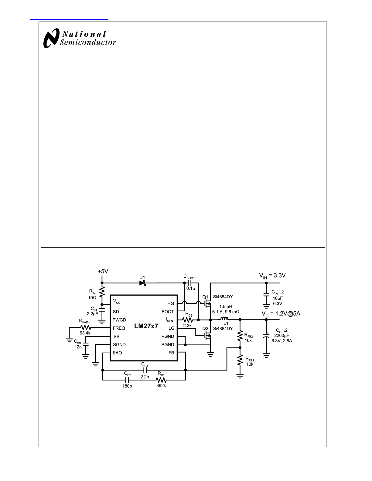
Typical Application
Features
n Input power from 2.2V to 16V
n Output voltage adjustable down to 0.6V
n Power Good flag, adjustable soft-start and output enable
for easy power sequencing
n Output over-voltage and under-voltage latch-off
(LM2727)
n Output over-voltage and under-voltage flag (LM2737)
n Reference Accuracy: 1.5% (0˚C - 125˚C)
n Current limit without sense resistor
n Soft start
n Switching frequency from 50 kHz to 2 MHz
n TSSOP-14 package
Applications
n Cable Modems
n Set-Top Boxes/ Home Gateways
n DDR Core Power
n High-Efficiency Distributed Power
n Local Regulation of Core Power
20049410
© 2003 National Semiconductor Corporation DS200494 www.national.com
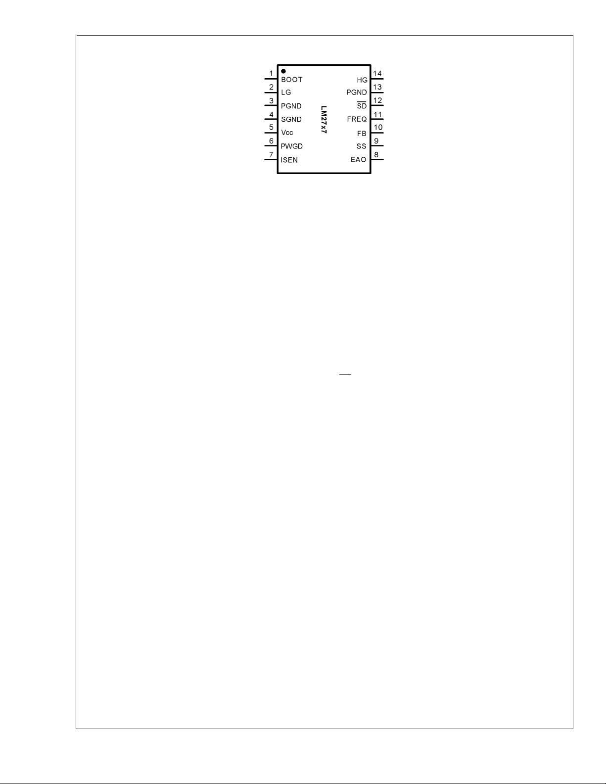
Connection Diagram
LM2727/LM2737
14-Lead Plastic TSSOP
θ
JA
NS Package Number MTC14
Pin Description
BOOT (Pin 1) - Supply rail for the N-channel MOSFET gate
drive. The voltage should be at least one gate threshold
above the regulator input voltage to properly turn on the
high-side N-FET.
LG (Pin 2) - Gate drive for the low-side N-channel MOSFET.
This signal is interlocked with HG to avoid shoot-through
problems.
PGND (Pins 3, 13) - Ground for FET drive circuitry. It should
be connected to system ground.
SGND (Pin 4) - Ground for signal level circuitry. It should be
connected to system ground.
(Pin 5) - Supply rail for the controller.
V
CC
PWGD (Pin 6) - Power Good. This is an open drain output.
The pin is pulled low when the chip is in UVP, OVP, or UVLO
mode. During normal operation, this pin is connected to V
or other voltage source through a pull-up resistor.
ISEN (Pin 7) - Current limit threshold setting. This sources a
fixed 50µA current. A resistor of appropriate value should be
connected between this pin and the drain of the low-side
FET.
CC
20049411
= 155˚C/W
EAO (Pin 8) - Output of the error amplifier. The voltage level
on this pin is compared with an internally generated ramp
signal to determine the duty cycle. This pin is necessary for
compensating the control loop.
SS (Pin 9) - Soft start pin. A capacitor connected between
this pin and ground sets the speed at which the output
voltage ramps up. Larger capacitor value results in slower
output voltage ramp but also lower inrush current.
FB (Pin 10) - This is the inverting input of the error amplifier,
which is used for sensing the output voltage and compensating the control loop.
FREQ (Pin 11) - The switching frequency is set by connecting a resistor between this pin and ground.
SD (Pin 12) - IC Logic Shutdown. When this pin is pulled low
the chip turns off the high side switch and turns on the low
side switch. While this pin is low, the IC will not start up. An
internal 20µA pull-up connects this pin to V
HG (Pin 14) - Gate drive for the high-side N-channel MOSFET. This signal is interlocked with LG to avoid shootthrough problems.
.
CC
www.national.com 2
LM2727/LM2737
Absolute Maximum Ratings (Note 1)
If Military/Aerospace specified devices are required,
Infrared or Convection (20sec) 235˚C
ESD Rating 2 kV
please contact the National Semiconductor Sales Office/
Distributors for availability and specifications.
Operating Ratings
V
CC
BOOTV 21V
Junction Temperature 150˚C
Storage Temperature −65˚C to 150˚C
Soldering Information
Lead Temperature
(soldering, 10sec) 260˚C
7V
Supply Voltage (VCC) 4.5V to 5.5V
Junction Temperature Range −40˚C to +125˚C
Thermal Resistance (θ
) 155˚C/W
JA
Electrical Characteristics
VCC= 5V unless otherwise indicated. Typicals and limits appearing in plain type apply for TA=TJ=+25˚C. Limits appearing in
boldface type apply over full Operating Temperature Range. Datasheet min/max specification limits are guaranteed by design,
test, or statistical analysis.
Symbol Parameter Conditions Min Typ Max Units
V
= 4.5V, 0˚C to +125˚C 0.591 0.6 0.609
CC
= 5V, 0˚C to +125˚C 0.591 0.6 0.609
V
CC
V
= 5.5V, 0˚C to +125˚C 0.591 0.6 0.609
V
FB_ADJ
V
I
t
PWGD1
t
PWGD2
I
SS-ON
I
SS-OC
ON
Q-V5
I
SD
FB Pin Voltage
UVLO Thresholds Rising
Operating VCCCurrent
Shutdown V
Current SD = 0V 0.15 0.4 0.7 mA
CC
PWGD Pin Response Time FB Voltage Going Up 6 µs
PWGD Pin Response Time FB Voltage Going Down 6 µs
SD Pin Internal Pull-up Current 20 µA
SS Pin Source Current SS Voltage = 2.5V
SS Pin Sink Current During Over
Current
I
Pin Source Current Trip
I
SEN-TH
SEN
Point
ERROR AMPLIFIER
GBW Error Amplifier Unity Gain
Bandwidth
G Error Amplifier DC Gain 60 dB
SR Error Amplifier Slew Rate 6 V/µA
I
I
FB
EAO
FB Pin Bias Current FB = 0.55V
EAO Pin Current Sourcing and
Sinking
V
EA
Error Amplifier Maximum Swing Minimum
CC
V
= 4.5V, −40˚C to +125˚C 0.589 0.6 0.609
CC
V
= 5V, −40˚C to +125˚C 0.589 0.6 0.609
CC
V
= 5.5V, −40˚C to +125˚C 0.589 0.6 0.609
CC
4.2
Falling
SD = 5V, FB = 0.55V
Fsw = 600kHz
SD = 5V, FB = 0.65V
Fsw = 600kHz
0˚C to +125˚C
-40˚C to +125˚C
SS Voltage = 2.5V
0˚C to +125˚C
-40˚C to +125˚C
1 1.5 2
0.8 1.7 2.2
8
5
35
28
3.6
11
11
95 µA
50
50
5 MHz
FB = 0.65V
V
= 2.5, FB = 0.55V
EAO
= 2.5, FB = 0.65V
V
EAO
0
0
15
30
2.8
0.8
1.2
Maximum
3.2
15
15
65
65
100
155
V
V
mA
µA
µA
nA
mA
V
www.national.com3
Electrical Characteristics (Continued)
VCC= 5V unless otherwise indicated. Typicals and limits appearing in plain type apply for TA=TJ=+25˚C. Limits appearing in
boldface type apply over full Operating Temperature Range. Datasheet min/max specification limits are guaranteed by design,
test, or statistical analysis.
Symbol Parameter Conditions Min Typ Max Units
LM2727/LM2737
GATE DRIVE
I
Q-BOOT
R
DS1
R
DS2
R
DS3
R
DS4
OSCILLATOR
f
OSC
D Max Duty Cycle f
LOGIC INPUTS AND OUTPUTS
V
SD-IH
V
SD-IL
V
PWGD-TH-LO
V
PWGD-TH-HI
V
PWGD-HYS
Note 1: Absolute maximum ratings indicate limits beyond which damage to the device may occur. Operating ratings indicate conditions for which the device
operates correctly. Opearting Ratings do not imply guaranteed performance limits.
Note 2: The human body model is a 100pF capacitor discharged through a 1.5k resistor into each pin.
BOOT Pin Quiescent Current BOOTV = 12V, EN = 0
Top FET Driver Pull-Up ON
resistance
Top FET Driver Pull-Down ON
resistance
Bottom FET Driver Pull-Up ON
resistance
Bottom FET Driver Pull-Down
ON resistance
PWM Frequency
0˚C to +125˚C
-40˚C to +125˚C
@
BOOT-SW = 5V
BOOT-SW = 5V
BOOT-SW = 5V
BOOT-SW = 5V
R
= 590kΩ 50
FADJ
= 88.7kΩ 300
R
FADJ
R
= 42.2kΩ, 0˚C to +125˚C 500 600 700
FADJ
R
= 42.2kΩ, -40˚C to +125˚C 490 600 700
FADJ
R
= 17.4kΩ 1400
FADJ
R
= 11.3kΩ 2000
FADJ
= 300kHz
PWM
= 600kHz
f
PWM
350mA 3 Ω
@
350mA 2 Ω
@
350mA 3 Ω
@
350mA 2 Ω
95
95
90
88
SD Pin Logic High Trip Point 2.6 3.5 V
SD Pin Logic Low Trip Point 0˚C to +125˚C
-40˚C to +125˚C
1.3
1.25
1.6
1.6
PWGD Pin Trip Points FB Voltage Going Down
0˚C to +125˚C
-40˚C to +125˚C
0.413
0.410
0.430
0.430
0.446
0.446
PWGD Pin Trip Points FB Voltage Going Up
0˚C to +125˚C
-40˚C to +125˚C
PWGD Hysteresis (LM2737 only) FB Voltage Going Down FB Voltage
Going Up
0.691
0.688
0.710
0.710
35
110
0.734
0.734
160
215
µA
kHz
%
V
V
V
mV
www.national.com 4
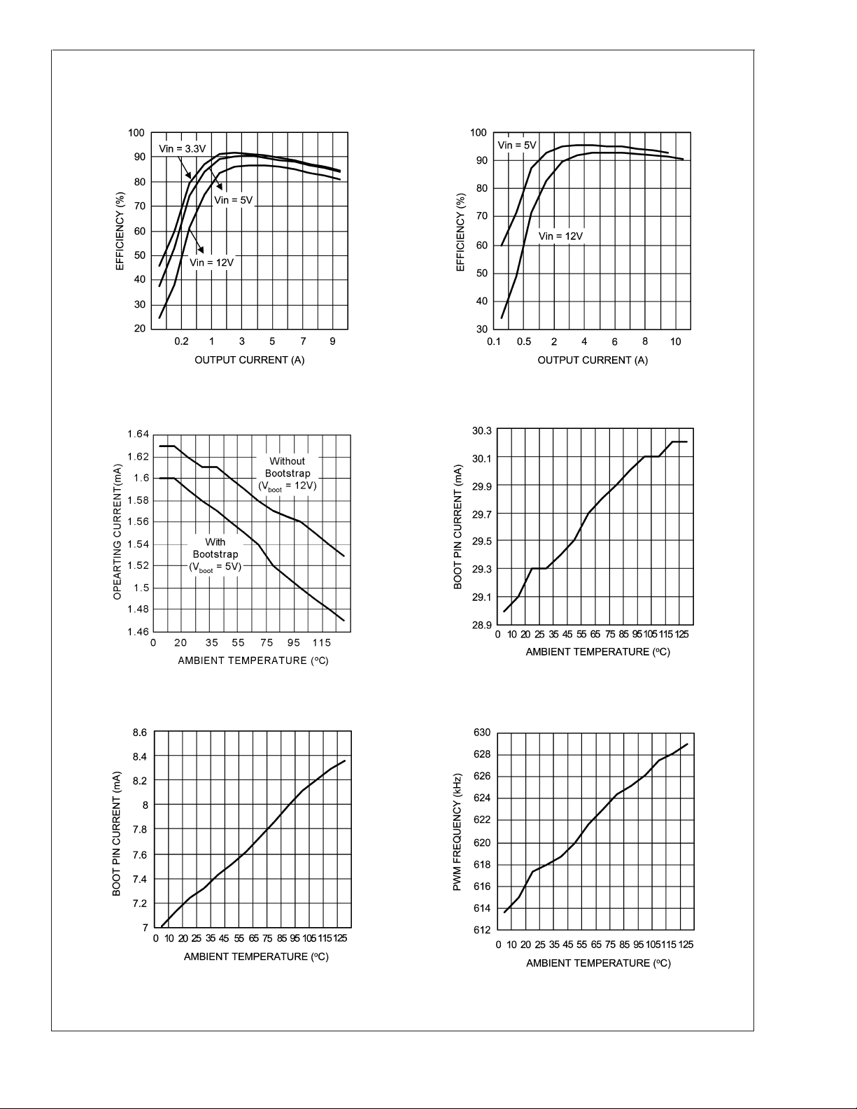
Typical Performance Characteristics
LM2727/LM2737
Efficiency (VO= 1.5V)
= 300kHz, TA= 25˚C
F
SW
20049412 20049413
VCCOperating Current vs Temperature
= 600kHz, No-Load
F
SW
Efficiency (V
= 300kHz, TA= 25˚C
F
SW
= 3.3V)
O
Bootpin Current vs Temperature for BOOTV = 12V
FSW= 600kHz, Si4826DY FET, No-Load
20049414
Bootpin Current vs Temperature with 5V Bootstrap
= 600kHz, Si4826DY FET, No-Load
F
SW
20049416
PWM Frequency vs Temperature
for R
FADJ
= 43.2kΩ
20049415
20049417
www.national.com5
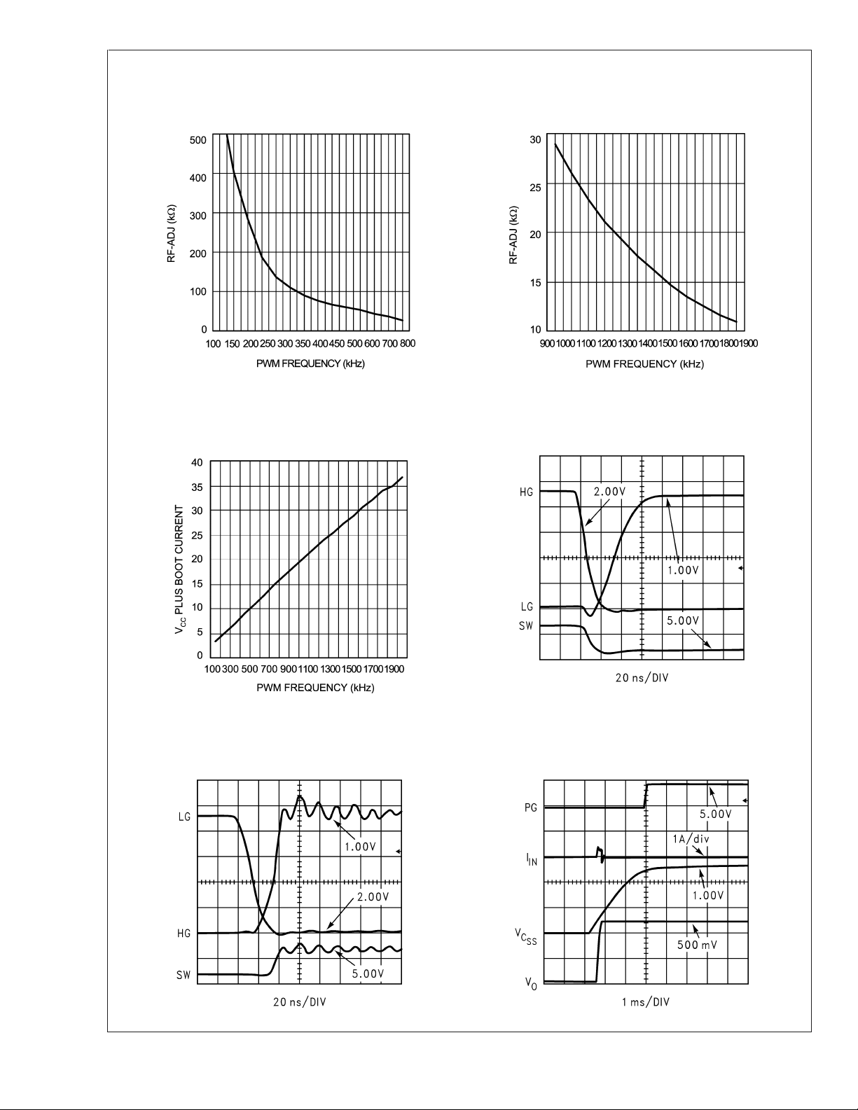
Typical Performance Characteristics (Continued)
(in 100 to 800kHz range), T
LM2727/LM2737
VCCOperating Current Plus Boot Current vs
PWM Frequency (Si4826DY FET, T
R
vs PWM Frequency
FADJ
= 25˚C
A
R
vs PWM Frequency
FADJ
(in 900 to 2000kHz range), T
20049418 20049419
A
Switch Waveforms (HG Falling)
V
= 5V, VO= 1.8V
IN
= 3A, CSS= 10nF
I
= 25˚C)
A
O
F
SW
= 600kHz
= 25˚C
20049420
Switch Waveforms (HG Rising)
= 5V, VO= 1.8V
V
IN
= 3A, FSW= 600kHz
I
O
20049424 20049421
www.national.com 6
Start-Up (No-Load)
V
= 10V, VO= 1.2V
IN
= 10nF, FSW= 300kHz
C
SS
20049423
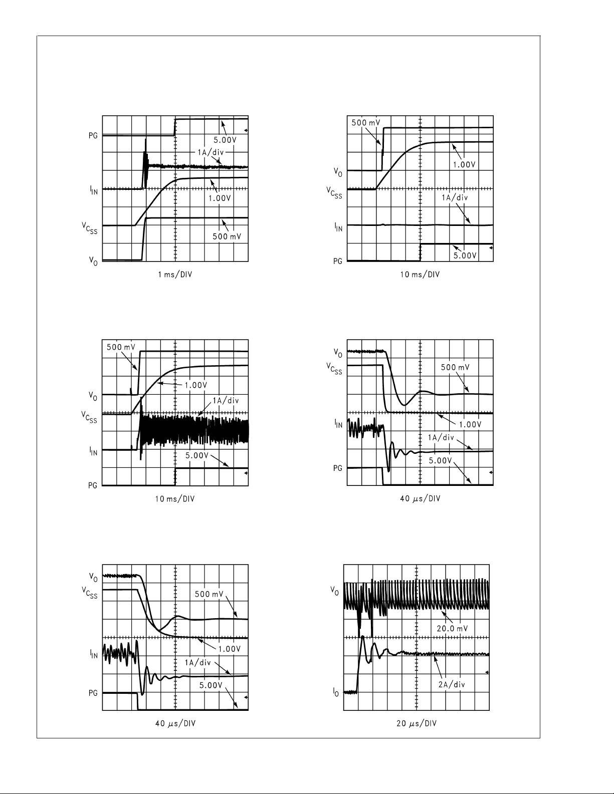
Typical Performance Characteristics (Continued)
Start-Up (Full-Load)
V
= 10V, VO= 1.2V
IN
= 10A, CSS= 10nF
I
O
Start Up (Full Load, 10x CSS)
V
I
O
= 300kHz
F
SW
= 10V, VO= 1.2V
IN
= 10A, CSS= 100nF
= 300kHz
F
SW
20049422 20049426
Start Up (No-Load, 10x C
= 10V, VO= 1.2V
V
IN
= 100nF, FSW= 300kHz
C
SS
Shutdown
V
= 10V, VO= 1.2V
IN
= 10A, CSS= 10nF
I
O
F
SW
= 300kHz
LM2727/LM2737
)
SS
Start Up (Full Load, 10x CSS)
= 10V, VO= 1.2V
V
IN
= 10A, CSS= 100nF
I
O
F
SW
= 300kHz
20049425
Load Transient Response (I
= 12V, VO= 1.2V
V
IN
= 300kHz
F
SW
20049433 20049428
=0to4A)
O
20049427
www.national.com7

Typical Performance Characteristics (Continued)
Load Transient Response (I
LM2727/LM2737
Line Transient Response (VIN=12V to 5V)
= 12V, VO= 1.2V
V
IN
= 300kHz
F
SW
= 1.2V, IO=5A
V
O
= 300kHz
F
SW
=4to0A)
O
20049429 20049430
Line Transient Response (V
= 1.2V, IO=5A
V
O
= 300kHz
F
SW
Line Transient Response
V
= 1.2V, IO=5A
O
= 300kHz
F
SW
=5V to 12V)
IN
20049431 20049432
www.national.com 8

Block Diagram
LM2727/LM2737
Application Information
THEORY OF OPERATION
The LM2727 is a voltage-mode, high-speed synchronous
buck regulator with a PWM control scheme. It is designed for
use in set-top boxes, thin clients, DSL/Cable modems, and
other applications that require high efficiency buck converters. It has power good (PWRGD), output shutdown (SD),
over voltage protection (OVP) and under voltage protection
(UVP). The over-voltage and under-voltage signals are OR
gated to drive the Power Good signal and a shutdown latch,
which turns off the high side gate and turns on the low side
gate if pulled low. Current limit is achieved by sensing the
voltage V
high side gate is turned off and the low side gate turned on.
The soft start capacitor is discharged by a 95µA source
(reducing the maximum duty cycle) until the current is under
control. The LM2737 does not latch off during UVP or OVP,
and uses the HIGH and LOW comparators for the powergood function only.
START UP
When V
high the soft start capacitor begins charging through an
internal fixed 10µA source. During this time the output of the
error amplifier is allowed to rise with the voltage of the soft
start capacitor. This capacitor, Css, determines soft start
time, and can be determined approximately by:
across the low side FET. During current limit the
DS
exceeds 4.2V and the enable pin EN sees a logic
CC
20049401
An application for a microprocessor might need a delay of
3ms, in which case C
would be 12nF. For a different
SS
device, a 100ms delay might be more appropriate, in which
case C
would be 400nF. (390 10%) During soft start the
SS
PWRGD flag is forced low and is released when the voltage
reaches a set value. At this point this chip enters normal
operation mode, the Power Good flag is released, and the
OVP and UVP functions begin to monitor Vo.
NORMAL OPERATION
While in normal operation mode, the LM2727/37 regulates
the output voltage by controlling the duty cycle of the high
side and low side FETs. The equation governing output
voltage is:
The PWM frequency is adjustable between 50kHz and
2MHz and is set by an external resistor, R
, between the
FADJ
FREQ pin and ground. The resistance needed for a desired
frequency is approximately:
www.national.com9

Application Information (Continued)
LM2727/LM2737
MOSFET GATE DRIVERS
The LM2727/37 has two gate drivers designed for driving
N-channel MOSFETs in a synchronous mode. Power for the
drivers is supplied through the BOOTV pin. For the high side
gate (HG) to fully turn on the top FET, the BOOTV voltage
must be at least one V
2*Vin) This voltage can be supplied by a separate, higher
voltage source, or supplied from a local charge pump structure. In a system such as a desktop computer, both 5V and
12V are usually available. Hence if Vin was 5V, the 12V
supply could be used for BOOTV. 12V is more than 2*Vin, so
the HG would operate correctly. For a BOOTV of 12V, the
initial gate charging current is 2A, and the initial gate discharging current is typically 6A.
FIGURE 1. BOOTV Supplied by Charge Pump
In a system without a separate, higher voltage, a charge
pump (bootstrap) can be built using a diode and small capacitor, Figure 1. The capacitor serves to maintain enough
voltage between the top FET gate and source to control the
device even when the top FET is on and its source has risen
up to the input voltage level.
The LM2727/37 gate drives use a BiCMOS design. Unlike
some other bipolar control ICs, the gate drivers have rail-torail swing, ensuring no spurious turn-on due to capacitive
coupling.
POWER GOOD SIGNAL
The power good signal is the or-gated flag representing
over-voltage and under-voltage protection. If the output voltage is 18% over it’s nominal value, V
below that value, V
= 0.41V, the power good flag goes low.
FB
The converter then turns off the high side gate, and turns on
the low side gate. Unlike the output (LM2727 only) the power
good flag is not latched off. It will return to a logic high
whenever the feedback pin voltage is between 70% and
118% of 0.6V.
greater than Vin. (BOOTV ≥
GS(th)
20049402
= 0.7V, or falls 30%
FB
until V
rises above 4.2V. As with shutdown, the soft start
CC
capacitor is discharged through a FET, ensuring that the next
start-up will be smooth.
CURRENT LIMIT
Current limit is realized by sensing the voltage across the
low side FET while it is on. The R
of the FET is a known
DSON
value, hence the current through the FET can be determined
as:
=I*R
V
DS
DSON
The current limit is determined by an external resistor, RCS,
connected between the switch node and the ISEN pin. A
constant current of 50µA is forced through Rcs, causing a
fixed voltage drop. This fixed voltage is compared against
and if the latter is higher, the current limit of the chip has
V
DS
been reached. R
can be found by using the following:
CS
R
CS=RDSON
(LOW) * I
LIM
/50µA
For example, a conservative 15A current limit in a 10A
design with a minimum R
of 10mΩ would require a
DSON
3.3kΩ resistor. Because current sensing is done across the
low side FET, no minimum high side on-time is necessary. In
the current limit mode the LM2727/37 will turn the high side
off and the keep low side on for as long as necessary. The
chip also discharges the soft start capacitor through a fixed
95µA source. In this way, smooth ramping up of the output
voltage as with a normal soft start is ensured. The output of
the LM2727/37 internal error amplifier is limited by the voltage on the soft start capacitor. Hence, discharging the soft
start capacitor reduces the maximum duty cycle D of the
controller. During severe current limit, this reduction in duty
cycle will reduce the output voltage, if the current limit conditions lasts for an extended time.
During the first few nanoseconds after the low side gate
turns on, the low side FET body diode conducts. This causes
an additional 0.7V drop in V
much lower. For example, if R
current through the FET was 10A, V
. The range of VDSis normally
DS
were 10mΩ and the
DSON
would be 0.1V. The
DS
current limit would see 0.7V as a 70A current and enter
current limit immediately. Hence current limit is masked during the time it takes for the high side switch to turn off and the
low side switch to turn on.
UVP/OVP
The output undervoltage protection and overvoltage protection mechanisms engage at 70% and 118% of the target
output voltage, respectively. In either case, the LM2727 will
turn off the high side switch and turn on the low side switch,
and discharge the soft start capacitor through a MOSFET
switch. The chip remains in this state until the shutdown pin
has been pulled to a logic low and then released. The UVP
function is masked only during the first charging of the soft
start capacitor, when voltage is first applied to the V
CC
pin. In
contrast, the LM2737 is designed to continue operating during UVP or OVP conditions, and to resume normal operation
once the fault condition is cleared. As with the LM2727, the
powergood flag goes low during this time, giving a logic-level
warning signal.
UVLO
The 4.2V turn-on threshold on V
of 0.6V. Therefore, if V
drops below 3.6V, the chip enters
CC
has a built in hysteresis
CC
UVLO mode. UVLO consists of turning off the top FET,
turning on the bottom FET, and remaining in that condition
www.national.com 10
SHUT DOWN
If the shutdown pin SD is pulled low, the LM2727/37 discharges the soft start capacitor through a MOSFET switch.
The high side switch is turned off and the low side switch is
turned on. The LM2727/37 remains in this state until SD is
released.

Application Information (Continued)
DESIGN CONSIDERATIONS
The following is a design procedure for all the components
needed to create the circuit shown in Figure 3 in the Example Circuits section, a 5V in to 1.2V out converter, capable
of delivering 10A with an efficiency of 85%. The switching
frequency is 300kHz. The same procedures can be followed
to create the circuit shown in Figure 3, Figure 4, and to
create many other designs with varying input voltages, output voltages, and output currents.
INPUT CAPACITOR
The input capacitors in a Buck switching converter are subjected to high stress due to the input current waveform,
which is a square wave. Hence input caps are selected for
their ripple current capability and their ability to withstand the
heat generated as that ripple current runs through their ESR.
Input rms ripple current is approximately:
The power dissipated by each input capacitor is:
Here, n is the number of capacitors, and indicates that power
loss in each cap decreases rapidly as the number of input
caps increase. The worst-case ripple for a Buck converter
occurs during full load, when the duty cycle D = 50%.
In the 5V to 1.2V case, D = 1.2/5 = 0.24. With a 10A
maximum load the ripple current is 4.3A. The Sanyo
10MV5600AX aluminum electrolytic capacitor has a ripple
current rating of 2.35A, up to 105˚C. Two such capacitors
make a conservative design that allows for unequal current
sharing between individual caps. Each capacitor has a maximum ESR of 18mΩ at 100 kHz. Power loss in each device is
then 0.05W, and total loss is 0.1W. Other possibilities for
input and output capacitors include MLCC, tantalum,
OSCON, SP, and POSCAPS.
INPUT INDUCTOR
The input inductor serves two basic purposes. First, in high
power applications, the input inductor helps insulate the
input power supply from switching noise. This is especially
important if other switching converters draw current from the
same supply. Noise at high frequency, such as that developed by the LM2727 at 1MHz operation, could pass through
the input stage of a slower converter, contaminating and
possibly interfering with its operation.
An input inductor also helps shield the LM2727 from high
frequency noise generated by other switching converters.
The second purpose of the input inductor is to limit the input
current slew rate. During a change from no-load to full-load,
the input inductor sees the highest voltage change across it,
equal to the full load current times the input capacitor ESR.
This value divided by the maximum allowable input current
slew rate gives the minimum input inductance:
In the case of a desktop computer system, the input current
slew rate is the system power supply or "silver box" output
current slew rate, which is typically about 0.1A/µs. Total input
capacitor ESR is 9mΩ, hence ∆V is 10*0.009 = 90 mV, and
the minimum inductance required is 0.9µH. The input inductor should be rated to handle the DC input current, which is
approximated by:
In this case I
is about 2.8A. One possible choice is the
IN-DC
TDK SLF12575T-1R2N8R2, a 1.2µH device that can handle
8.2Arms, and has a DCR of 7mΩ.
OUTPUT INDUCTOR
The output inductor forms the first half of the power stage in
a Buck converter. It is responsible for smoothing the square
wave created by the switching action and for controlling the
output current ripple. (∆I
) The inductance is chosen by
o
selecting between tradeoffs in efficiency and response time.
The smaller the output inductor, the more quickly the converter can respond to transients in the load current. As
shown in the efficiency calculations, however, a smaller inductor requires a higher switching frequency to maintain the
same level of output current ripple. An increase in frequency
can mean increasing loss in the FETs due to the charging
and discharging of the gates. Generally the switching frequency is chosen so that conduction loss outweighs switching loss. The equation for output inductor selection is:
Plugging in the values for output current ripple, input voltage,
output voltage, switching frequency, and assuming a 40%
peak-to-peak output current ripple yields an inductance of
1.5µH. The output inductor must be rated to handle the peak
current (also equal to the peak switch current), which is (Io +
). This is 12A for a 10A design. The Coilcraft D05022-
0.5*∆I
o
152HC is 1.5µH, is rated to 15Arms, and has a DCR of 4mΩ.
OUTPUT CAPACITOR
The output capacitor forms the second half of the power
stage of a Buck switching converter. It is used to control the
output voltage ripple (∆V
) and to supply load current during
o
fast load transients.
In this example the output current is 10A and the expected
type of capacitor is an aluminum electrolytic, as with the
input capacitors. (Other possibilities include ceramic, tantalum, and solid electrolyte capacitors, however the ceramic
type often do not have the large capacitance needed to
supply current for load transients, and tantalums tend to be
more expensive than aluminum electrolytic.) Aluminum capacitors tend to have very high capacitance and fairly low
ESR, meaning that the ESR zero, which affects system
stability, will be much lower than the switching frequency.
The large capacitance means that at switching frequency,
the ESR is dominant, hence the type and number of output
capacitors is selected on the basis of ESR. One simple
formula to find the maximum ESR based on the desired
output voltage ripple, ∆V
ripple, ∆I
o
, is:
and the designed output current
o
LM2727/LM2737
www.national.com11

Application Information (Continued)
LM2727/LM2737
In this example, in order to maintain a 2% peak-to-peak
output voltage ripple and a 40% peak-to-peak inductor current ripple, the required maximum ESR is 6mΩ. Three Sanyo
10MV5600AX capacitors in parallel will give an equivalent
ESR of 6mΩ. The total bulk capacitance of 16.8mF is
enough to supply even severe load transients. Using the
same capacitors for both input and output also keeps the bill
of materials simple.
MOSFETS
MOSFETS are a critical part of any switching controller and
have a direct impact on the system efficiency. In this case
the target efficiency is 85% and this is the variable that will
determine which devices are acceptable. Loss from the capacitors, inductors, and the LM2727 itself are detailed in the
Efficiency section, and come to about 0.54W. To meet the
target efficiency, this leaves 1.45W for the FET conduction
loss, gate charging loss, and switching loss. Switching loss
is particularly difficult to estimate because it depends on
many factors. When the load current is more than about 1 or
2 amps, conduction losses outweigh the switching and gate
charging losses. This allows FET selection based on the
of the FET. Adding the FET switching and gate-
R
DSON
charging losses to the equation leaves 1.2W for conduction
losses. The equation for conduction loss is:
P
Cnd
The factor k is a constant which is added to account for the
increasing R
Si4442DY has a typical R
the equation for P
design were for a 5V to 2.5V circuit, an equal number of
FETs on the high and low sides would be the best solution.
With the duty cycle D = 0.24, it becomes apparent that the
low side FET carries the load current 76% of the time.
Adding a second FET in parallel to the bottom FET could
improve the efficiency by lowering the effective R
lower the duty cycle, the more effective a second or even
third FET can be. For a minimal increase in gate charging
loss (0.054W) the decrease in conduction loss is 0.15W.
What was an 85% design improves to 86% for the added
cost of one SO-8 MOSFET.
CONTROL LOOP COMPONENTS
The circuit is this design example and the others shown in
the Example Circuits section have been compensated to
improve their DC gain and bandwidth. The result of this
compensation is better line and load transient responses.
For the LM2727, the top feedback divider resistor, Rfb2, is
also a part of the compensation. For the 10A, 5V to 1.2V
design, the values are:
Cc1 = 4.7pF 10%, Cc2 = 1nF 10%, Rc = 229kΩ 1%. These
values give a phase margin of 63˚ and a bandwidth of
29.3kHz.
2
= D(I
*R
o
of a FET due to heating. Here, k = 1.3. The
DSON
CND
*k) + (1-D)(I
DSON
of 4.1mΩ. When plugged into
DSON
the result is a loss of 0.533W. If this
2
*R
o
DSON
DSON
*k)
. The
Rbypass and Cbypass are standard filter components designed to ensure smooth DC voltage for the chip supply and
for the bootstrap structure, if it is used. Use 10Ω for the
resistor and a 2.2µF ceramic for the cap. Cb is the bootstrap
capacitor, and should be 0.1µF. (In the case of a separate,
higher supply to the BOOTV pin, this 0.1µF cap can be used
to bypass the supply.) Using a Schottky device for the bootstrap diode allows the minimum drop for both high and low
side drivers. The On Semiconductor BAT54 or MBR0520
work well.
Rp is a standard pull-up resistor for the open-drain power
good signal, and should be 10kΩ. If this feature is not
necessary, it can be omitted.
is the resistor used to set the current limit. Since the
R
CS
design calls for a peak current magnitude (Io + 0.5 * ∆I
)of
o
12A, a safe setting would be 15A. (This is well below the
saturation current of the output inductor, which is 25A.)
Following the equation from the Current Limit section, use a
3.3kΩ resistor.
is used to set the switching frequency of the chip.
R
FADJ
Following the equation in the Theory of Operation section,
the closest 1% tolerance resistor to obtain f
= 300kHz is
SW
88.7kΩ.
depends on the users requirements. Based on the
C
SS
equation for C
in the Theory of Operation section, for a
SS
3ms delay, a 12nF capacitor will suffice.
EFFICIENCY CALCULATIONS
A reasonable estimation of the efficiency of a switching
controller can be obtained by adding together the loss is
each current carrying element and using the equation:
The following shows an efficiency calculation to complement
the Circuit of Figure 3. Output power for this circuit is 1.2V x
10A = 12W.
Chip Operating Loss
P
IQ=IQ-V
*V
CC
CC
2mA x 5V = 0.01W
FET Gate Charging Loss
PGC=n*VCC*QGS*f
OSC
The value n is the total number of FETs used. The Si4442DY
has a typical total gate charge, Q
4.1mΩ. For a single FET on top and bottom:
2*5*36E
-9
*300,000 = 0.108W
, of 36nC and an r
GS
ds-on
FET Switching Loss
=0.5*Vin*IO*(tr+tf)* f
P
SW
The Si4442DY has a typical rise time trand fall time tfof 11
and 47ns, respectively. 0.5*5*10*58E
OSC
-9
*300,000 = 0.435W
of
SUPPORT CAPACITORS AND RESISTORS
The Cinx capacitors are high frequency bypass devices,
designed to filter harmonics of the switching frequency and
input noise. Two 1µF ceramic capacitors with a sufficient
voltage rating (10V for the Circuit of Figure 3) will work well
in almost any case.
www.national.com 12

Application Information (Continued)
FET Conduction Loss
P
= 0.533W
Cn
Input Capacitor Loss
4.282*0.018/2 = 0.084W
Example Circuits
Input Inductor Loss
P
Lin
2.822*0.007 = 0.055W
Output Inductor Loss
P
Lout
102*0.004 = 0.4W
System Efficiency
=I
=I
2
in
2
o
* DCR
* DCR
LM2727/LM2737
input-L
output-L
FIGURE 2. 5V-16V to 3.3V, 10A, 300kHz
This circuit and the one featured on the front page have been
designed to deliver high current and high efficiency in a small
package, both in area and in height The tallest component in
20049403
this circuit is the inductor L1, which is 6mm tall. The compensation has been designed to tolerate input voltages from
5 to 16V.
www.national.com13

Example Circuits (Continued)
LM2727/LM2737
FIGURE 3. 5V to 1.2V, 10A, 300kHz
This circuit design, detailed in the Design Considerations
section, uses inexpensive aluminum capacitors and off-theshelf inductors. It can deliver 10A at better than 85% efficiency. Large bulk capacitance on input and output ensure
stable operation.
20049404
FIGURE 4. 5V to 1.8V, 3A, 600kHz
The example circuit of Figure 4 has been designed for
minimum component count and overall solution size. A
switching frequency of 600kHz allows the use of small input/
output capacitors and a small inductor. The availability of
separate 5V and 12V supplies (such as those available from
desk-top computer supplies) and the low current further
www.national.com 14
20049405
reduce component count. Using the 12V supply to power the
MOSFET drivers eliminates the bootstrap diode, D1. At low
currents, smaller FETs or dual FETs are often the most
efficient solutions. Here, the Si4826DY, an asymmetric dual
FET in an SO-8 package, yields 92% efficiency at a load of
2A.

Example Circuits (Continued)
LM2727/LM2737
20049406
FIGURE 5. 3.3V to 0.8V, 5A, 500kHz
The circuit of Figure 5 demonstrates the LM2727 delivering a
low output voltage at high efficiency (87%) A separate 5V
supply is required to run the chip, however the input voltage
can be as low as 2.2
www.national.com15

Example Circuits (Continued)
LM2727/LM2737
FIGURE 6. 1.8V and 3.3V, 1A, 1.4MHz, Simultaneous
The circuits in Figure 6 are intended for ADSL applications,
where the high switching frequency keeps noise out of the
data transmission range. In this design, the 1.8 and 3.3V
outputs come up simultaneously by using the same softstart
capacitor. Because two current sources now charge the
same capacitor, the capacitance must be doubled to achieve
the same softstart time. (Here, 40nF is used to achieve a
www.national.com 16
20049407
5ms softstart time.) A common softstart capacitor means
that, should one circuit enter current limit, the other circuit
will also enter current limit. In addition, if both circuits are
built with the LM2727, a UVP or OVP fault on one circuit will
cause both circuits to latch off. The additional compensation
components Rc2 and Cc3 are needed for the low ESR, all
ceramic output capacitors, and the wide (3x) range of Vin.

Example Circuits (Continued)
LM2727/LM2737
20049408
FIGURE 7. 12V Unregulated to 3.3V, 3A, 750kHz
This circuit shows the LM27x7 paired with a cost effective
solution to provide the 5V chip power supply, using no extra
components other than the LM78L05 regulator itself. The
input voltage comes from a ’brick’ power supply which does
not regulate the 12V line tightly. Additional, inexpensive 10uF
ceramic capacitors (Cinx and Cox) help isolate devices with
sensitive databands, such as DSL and cable modems, from
switching noise and harmonics.
20049409
FIGURE 8. 12V to 5V, 1.8A, 100kHz
In situations where low cost is very important, the LM27x7
can also be used as an asynchronous controller, as shown in
the above circuit. Although a a schottky diode in place of the
bottom FET will not be as efficient, it will cost much less than
the FET. The 5V at low current needed to run the LM27x7
could come from a zener diode or inexpensive regulator,
such as the one shown in Figure 7. Because the LM27x7
senses current in the low side MOSFET, the current limit
feature will not function in an asynchronous design. The
ISEN pin should be left open in this case.
www.national.com17

TABLE 1. Bill of Materials for Typical Application Circuit
ID Part Number Type Size Parameters Qty. Vendor
U1 LM2727
Q1, Q2 Si4884DY N-MOSFET SO-8 30V, 4.1mΩ, 36nC 1 Vishay
LM2727/LM2737
L1 RLF7030T-1R5N6R1 Inductor 7.1x7.1x3.2mm 1.5µH, 6.1A 9.6mΩ 1 TDK
Cin1, Cin2 C2012X5R1J106M MLCC 0805 10µF 6.3V 2 TDK
Cinx C3216X7R1E105K Capacitor 1206 1µF, 25V 1 TDK
Co1, Co2 6MV2200WG AL-E 10mm D 20mm H 2200µF 6.3V125mΩ 2 Sanyo
Cboot VJ1206X104XXA Capacitor 1206 0.1µF, 25V 1 Vishay
Cin C3216X7R1E225K Capacitor 1206 0.1µF, 25V 1 TDK
Css VJ1206X123KXX Capacitor 1206 12nF, 25V 1 Vishay
Cc1 VJ1206A2R2KXX Capacitor 1206 2.2pF 10% 1 Vishay
Cc2 VJ1206A181KXX Capacitor 1206 180pF 10% 1 Vishay
Rin CRCW1206100J Resistor 1206 10Ω 5% 1 Vishay
Rfadj CRCW12066342F Resistor 1206 63.4kΩ 1% 1 Vishay
Rc1 CRCW12063923F Resistor 1206 392kΩ 1% 1 Vishay
Rfb1 CRCW12061002F Resistor 1206 10kΩ 1% 1 Vishay
Rfb2 CRCW12061002F Resistor 1206 10kΩ 1% 1 Vishay
Rcs CRCW1206222J Resistor 1206 2.2kΩ 5% 1 Vishay
ID Part Number Type Size Parameters Qty. Vendor
L1 RLF12560T-2R7N110 Inductor 12.5x12.8x6mm 2.7µH, 14.4A 4.5mΩ 1 TDK
Co1, Co2,
Co3, Co4
Cc1 VJ1206A6R8KXX Capacitor 1206 6.8pF 10% 1 Vishay
Cc2 VJ1206A271KXX Capacitor 1206 270pF 10% 1 Vishay
Cc3 VJ1206A471KXX Capacitor 1206 470pF 10% 1 Vishay
Rc2 CRCW12068451F Resistor 1206 8.45kΩ 1% 1 Vishay
Rfb1 CRCW12061102F Resistor 1206 11kΩ 1% 1 Vishay
10TPB100M POSCAP 7.3x4.3x2.8mm 100µF 10V 1.9Arms 4 Sanyo
Synchronous
Controller
TABLE 2. Bill of Materials for Circuit of Figure 2
(Identical to BOM for 1.5V except as noted below)
TSSOP-14 TSSOP-14 1 NSC
TABLE 3. Bill of Materials for Circuit of Figure 3
ID Part Number Type Size Parameters Qty. Vendor
U1 LM2727
Q1 Si4442DY N-MOSFET SO-8 30V, 4.1mΩ,
Q2 Si4442DY N-MOSFET SO-8 30V, 4.1mΩ,
D1 BAT-54 Schottky Diode SOT-23 30V 1 Vishay
Lin SLF12575T-1R2N8R2 Inductor 12.5x12.5x7.5mm 12µH, 8.2A, 6.9mΩ 1 Coilcraft
L1 D05022-152HC Inductor 22.35x16.26x8mm 1.5µH, 15A,4mΩ 1 Coilcraft
Cin1, Cin2 10MV5600AX
Cinx C3216X7R1E105K Capacitor 1206 1µF, 25V 1 TDK
Co1, Co2,
Co3
Cboot VJ1206X104XXA Capacitor 1206 0.1µF, 25V 1 Vishay
Cin C3216X7R1E225K Capacitor 1206 2.2µF, 25V 1 TDK
Css VJ1206X123KXX Capacitor 1206 12nF, 25V 1 Vishay
www.national.com 18
10MV5600AX
Synchronous
Controller
Aluminum
Electrolytic
Aluminum
Electrolytic
TSSOP-14 1 NSC
@
4.5V,
36nC
@
4.5V,
36nC
16mm D 25mm H 5600µF10V 2.35Arms 2 Sanyo
16mm D 25mm H 5600µF10V 2.35Arms 2 Sanyo
1 Vishay
1 Vishay

TABLE 3. Bill of Materials for Circuit of Figure 3 (Continued)
ID Part Number Type Size Parameters Qty. Vendor
Cc1 VJ1206A4R7KXX Capacitor 1206 4.7pF 10% 1 Vishay
Cc2 VJ1206A102KXX Capacitor 1206 1nF 10% 1 Vishay
Rin CRCW1206100J Resistor 1206 10Ω 5% 1 Vishay
Rfadj CRCW12068872F Resistor 1206 88.7kΩ 1% 1 Vishay
Rc1 CRCW12062293F Resistor 1206 229kΩ 1% 1 Vishay
Rfb1 CRCW12064991F Resistor 1206 4.99kΩ 1% 1 Vishay
Rfb2 CRCW12064991F Resistor 1206 4.99kΩ 1% 1 Vishay
Rcs CRCW1206152J Resistor 1206 1.5kΩ 5% 1 Vishay
TABLE 4. Bill of Materials for Circuit of Figure 4
ID Part Number Type Size Parameters Qty. Vendor
U1 LM2727 Synchronous
Controller
Q1/Q2 Si4826DY Asymetric Dual
N-MOSFET
L1 DO3316P-222 Inductor 12.95x9.4x
Cin1 10TPB100ML POSCAP 7.3x4.3x3.1mm 100µF 10V 1.9Arms 1 Sanyo
Co1 4TPB220ML POSCAP 7.3x4.3x3.1mm 220µF 4V 1.9Arms 1 Sanyo
Cc C3216X7R1E105K Capacitor 1206 1µF, 25V 1 TDK
Cin C3216X7R1E225K Capacitor 1206 2.2µF, 25V 1 TDK
Css VJ1206X123KXX Capacitor 1206 12nF, 25V 1 Vishay
Cc1 VJ1206A100KXX Capacitor 1206 10pF 10% 1 Vishay
Cc2 VJ1206A561KXX Capacitor 1206 560pF 10% 1 Vishay
Rin CRCW1206100J Resistor 1206 10Ω 5% 1 Vishay
Rfadj CRCW12064222F Resistor 1206 42.2kΩ 1% 1 Vishay
Rc1 CRCW12065112F Resistor 1206 51.1kΩ 1% 1 Vishay
Rfb1 CRCW12062491F Resistor 1206 2.49kΩ 1% 1 Vishay
Rfb2 CRCW12064991F Resistor 1206 4.99kΩ 1% 1 Vishay
Rcs CRCW1206272J Resistor 1206 2.7kΩ 5% 1 Vishay
TSSOP-14 1 NSC
SO-8 30V, 24mΩ/ 8nC
Top 16.5mΩ/ 15nC
2.2µH, 6.1A, 12mΩ 1 Coilcraft
5.21mm
1 Vishay
LM2727/LM2737
TABLE 5. Bill of Materials for Circuit of Figure 5
ID Part Number Type Size Parameters Qty. Vendor
U1 LM2727 Synchronous
Controller
Q1 Si4884DY N-MOSFET SO-8 30V, 13.5mΩ,
Q2 Si4884DY N-MOSFET SO-8 30V, 13.5mΩ,
D1 BAT-54 Schottky Diode SOT-23 30V 1 Vishay
Lin P1166.102T Inductor 7.29x7.29 3.51mm 1µH, 11A 3.7mΩ 1 Pulse
L1 P1168.102T Inductor 12x12x4.5 mm 1µH, 11A, 3.7mΩ 1 Pulse
Cin1 10MV5600AX Aluminum
Electrolytic
Cinx C3216X7R1E105K Capacitor 1206 1µF, 25V 1 TDK
Co1, Co2,
Co3
Cboot VJ1206X104XXA Capacitor 1206 0.1µF, 25V 1 Vishay
Cin C3216X7R1E225K Capacitor 1206 2.2µF, 25V 1 TDK
Css VJ1206X123KXX Capacitor 1206 12nF, 25V 1 Vishay
16MV4700WX Aluminum
Electrolytic
TSSOP-14 1 NSC
@
4.5V
15.3nC
@
4.5V
15.3nC
16mm D 25mm H 5600µF 10V 2.35Arms 1 Sanyo
12.5mm D 30mmH4700µF 16V 2.8Arms 2 Sanyo
1 Vishay
1 Vishay
www.national.com19

TABLE 5. Bill of Materials for Circuit of Figure 5 (Continued)
ID Part Number Type Size Parameters Qty. Vendor
Cc1 VJ1206A4R7KXX Capacitor 1206 4.7pF 10% 1 Vishay
Cc2 VJ1206A681KXX Capacitor 1206 680pF 10% 1 Vishay
LM2727/LM2737
Rin CRCW1206100J Resistor 1206 10Ω 5% 1 Vishay
Rfadj CRCW12064992F Resistor 1206 49.9kΩ 1% 1 Vishay
Rc1 CRCW12061473F Resistor 1206 147kΩ 1% 1 Vishay
Rfb1 CRCW12061492F Resistor 1206 14.9kΩ 1% 1 Vishay
Rfb2 CRCW12064991F Resistor 1206 4.99kΩ 1% 1 Vishay
Rcs CRCW1206332J Resistor 1206 3.3kΩ 5% 1 Vishay
TABLE 6. Bill of Materials for Circuit of Figure 6
ID Part Number Type Size Parameters Qty. Vendor
U1 LM2727 Synchronous
Controller
Q1/Q2 Si4826DY Assymetric Dual
N-MOSFET
D1 BAT-54 Schottky Diode SOT-23 30V 1 Vishay
Lin RLF7030T-1R0N64 Inductor 6.8x7.1x3.2mm 1µH, 6.4A, 7.3mΩ 1 TDK
L1 RLF7030T-3R3M4R1 Inductor 6.8x7.1x3.2mm 3.3µH, 4.1A, 17.4mΩ 1 TDK
Cin1 C4532X5R1E156M MLCC 1812 15µF 25V 3.3Arms 1 Sanyo
Co1 C4532X5R1E156M MLCC 1812 15µF 25V 3.3Arms 1 Sanyo
Cboot VJ1206X104XXA Capacitor 1206 0.1µF, 25V 1 TDK
Cin C3216X7R1E225K Capacitor 1206 2.2µF, 25V 1 TDK
Css VJ1206X393KXX Capacitor 1206 39nF, 25V 1 Vishay
Cc1 VJ1206A220KXX Capacitor 1206 22pF 10% 1 Vishay
Cc2 VJ1206A681KXX Capacitor 1206 680pF 10% 1 Vishay
Cc3 VJ1206A681KXX Capacitor 1206 680pF 10% 1 Vishay
Rin CRCW1206100J Resistor 1206 10Ω 5% 1 Vishay
Rfadj CRCW12061742F Resistor 1206 17.4kΩ 1% 1 Vishay
Rc1 CRCW12061072F Resistor 1206 10.7kΩ 1% 1 Vishay
Rc2 CRCW120666R5F Resistor 1206 66.5Ω 1% 1 Vishay
Rfb1 CRCW12064991F Resistor 1206 4.99kΩ 1% 1 Vishay
Rfb2 CRCW12061002F Resistor 1206 10kΩ 1% 1 Vishay
Rcs CRCW1206152J Resistor 1206 1.5kΩ 5% 1 Vishay
TSSOP-14 1 NSC
SO-8 30V, 24mΩ/ 8nC
Top 16.5mΩ/ 15nC
1 Vishay
TABLE 7. Bill of Materials for 3.3V Circuit of Figure 6
(Identical to BOM for 1.8V except as noted below)
ID Part Number Type Size Parameters Qty. Vendor
L1 RLF7030T-4R7M3R4 Inductor 6.8x7.1x 3.2mm 4.7µH, 3.4A, 26mΩ 1 TDK
Cc1 VJ1206A270KXX Capacitor 1206 27pF 10% 1 Vishay
Cc2 VJ1206X102KXX Capacitor 1206 1nF 10% 1 Vishay
Cc3 VJ1206A821KXX Capacitor 1206 820pF 10% 1 Vishay
Rc1 CRCW12061212F Resistor 1206 12.1kΩ 1% 1 Vishay
Rc2 CRCW12054R9F Resistor 1206 54.9Ω 1% 1 Vishay
Rfb1 CRCW12062211F Resistor 1206 2.21kΩ 1% 1 Vishay
Rfb2 CRCW12061002F Resistor 1206 10kΩ 1% 1 Vishay
TABLE 8. Bill of Materials for Circuit of Figure 7
ID Part Number Type Size Parameters Qty. Vendor
U1 LM2727 Synchronous
Controller
www.national.com 20
TSSOP-14 1 NSC

TABLE 8. Bill of Materials for Circuit of Figure 7 (Continued)
ID Part Number Type Size Parameters Qty. Vendor
U2 LM78L05 Voltage
Regulator
Q1/Q2 Si4826DY Assymetric Dual
N-MOSFET
D1 BAT-54 Schottky Diode SOT-23 30V 1 Vishay
Lin RLF7030T-1R0N64 Inductor 6.8x7.1x3.2mm 1µH, 6.4A, 7.3mΩ 1 TDK
L1 SLF12565T-4R2N5R5 Inductor 12.5x12.5x6.5mm 4.2µH, 5.5A, 15mΩ 1 TDK
Cin1 16MV680WG Al-E D: 10mm L:
Cinx C3216X5R1C106M MLCC 1210 10µF 16V 3.4Arms 1 TDK
Co1 Co2 16MV680WG MLCC 1812 15µF 25V 3.3Arms 1 Sanyo
Cox C3216X5R10J06M MLCC 1206 10µF 6.3V 2.7A TDK
Cboot VJ1206X104XXA Capacitor 1206 0.1µF, 25V 1 Vishay
Cin C3216X7R1E225K Capacitor 1206 2.2µF, 25V 1 TDK
Css VJ1206X123KXX Capacitor 1206 12nF, 25V 1 Vishay
Cc1 VJ1206A8R2KXX Capacitor 1206 8.2pF 10% 1 Vishay
Cc2 VJ1206X102KXX Capacitor 1206 1nF 10% 1 Vishay
Cc3 VJ1206X472KXX Capacitor 1206 4.7nF 10% 1 Vishay
Rfadj CRCW12063252F Resistor 1206 32.5kΩ 1% 1 Vishay
Rc1 CRCW12065232F Resistor 1206 52.3kΩ 1% 1 Vishay
Rc2 CRCW120662371F Resistor 1206 2.37Ω 1% 1 Vishay
Rfb1 CRCW12062211F Resistor 1206 2.21kΩ 1% 1 Vishay
Rfb2 CRCW12061002F Resistor 1206 10kΩ 1% 1 Vishay
Rcs CRCW1206202J Resistor 1206 2kΩ 5% 1 Vishay
SO-8 1 NSC
SO-8 30V, 24mΩ/ 8nC
Top 16.5mΩ/ 15nC
680µF 16V 3.4Arms 1 Sanyo
12.5mm
1 Vishay
LM2727/LM2737
TABLE 9. Bill of Materials for Circuit of Figure 8
ID Part Number Type Size Parameters Qty. Vendor
U1 LM2727 Synchronous
Controller
Q1 Si4894DY N-MOSFET SO-8 30V, 15mΩ, 11.5nC 1 Vishay
D2 MBRS330T3 Schottky Diode SO-8 30V, 3A 1 ON
L1 SLF12565T-470M2R4 Inductor 12.5x12.8x 4.7mm 47µH, 2.7A 53mΩ 1 TDK
D1 MBR0520 Schottky Diode 1812 20V 0.5A 1 ON
Cin1 16MV680WG Al-E 1206 680µF, 16V, 1.54Arms 1 Sanyo
Cinx C3216X5R1C106M MLCC 1206 10µF, 16V, 3.4Arms 1 TDK
Co1, Co2 16MV680WG Al-E D: 10mm L:
Cox C3216X5R10J06M MLCC 1206 10µF, 6.3V 2.7A 1 TDK
Cboot VJ1206X104XXA Capacitor 1206 0.1µF, 25V 1 Vishay
Cin C3216X7R1E225K Capacitor 1206 2.2µF, 25V 1 TDK
Css VJ1206X123KXX Capacitor 1206 12nF, 25V 1 Vishay
Cc1 VJ1206A561KXX Capacitor 1206 56pF 10% 1 Vishay
Cc2 VJ1206X392KXX Capacitor 1206 3.9nF 10% 1 Vishay
Cc3 VJ1206X223KXX Capacitor 1206 22nF 10% 1 Vishay
Rfadj CRCW12062673F Resistor 1206 267kΩ 1% 1 Vishay
Rc1 CRCW12066192F Resistor 1206 61.9kΩ 1% 1 Vishay
Rc2 CRCW12067503F Resistor 1206 750kΩ 1% 1 Vishay
Rfb1 CRCW12061371F Resistor 1206 1.37kΩ 1% 1 Vishay
Rfb2 CRCW12061002F Resistor 1206 10kΩ 1% 1 Vishay
Rcs CRCW1206122F Resistor 1206 1.2kΩ 5% 1 Vishay
TSSOP-14 1 NSC
680µF 16V 26mΩ 2 Sanyo
12.5mm
www.national.com21

Physical Dimensions inches (millimeters) unless otherwise noted
TSSOP-14 Pin Package
NS Package Number MTC14
LIFE SUPPORT POLICY
NATIONAL’S PRODUCTS ARE NOT AUTHORIZED FOR USE AS CRITICAL COMPONENTS IN LIFE SUPPORT
DEVICES OR SYSTEMS WITHOUT THE EXPRESS WRITTEN APPROVAL OF THE PRESIDENT AND GENERAL
COUNSEL OF NATIONAL SEMICONDUCTOR CORPORATION. As used herein:
1. Life support devices or systems are devices or
systems which, (a) are intended for surgical implant
into the body, or (b) support or sustain life, and
whose failure to perform when properly used in
accordance with instructions for use provided in the
2. A critical component is any component of a life
support device or system whose failure to perform
can be reasonably expected to cause the failure of
the life support device or system, or to affect its
safety or effectiveness.
labeling, can be reasonably expected to result in a
significant injury to the user.
National Semiconductor
Americas Customer
Support Center
Email: new.feedback@nsc.com
Tel: 1-800-272-9959
www.national.com
National Semiconductor
Europe Customer Support Center
Fax: +49 (0) 180-530 85 86
Email: europe.support@nsc.com
Deutsch Tel: +49 (0) 69 9508 6208
English Tel: +44 (0) 870 24 0 2171
Français Tel: +33 (0) 1 41 91 8790
National Semiconductor
Asia Pacific Customer
Support Center
Email: ap.support@nsc.com
National Semiconductor
Japan Customer Support Center
Fax: 81-3-5639-7507
Email: jpn.feedback@nsc.com
Tel: 81-3-5639-7560
LM2727/LM2737 N-Channel FET Synchronous Buck Regulator Controller for Low Output Voltages
National does not assume any responsibility for use of any circuitry described, no circuit patent licenses are implied and National reserves the right at any time without notice to change said circuitry and specifications.
 Loading...