

LM27241
Synchronous Buck Regulator Controller for Mobile
Systems
LM27241 Synchronous Buck Regulator Controller for Mobile Systems
May 2005
General Description
The LM27241 is an adjustable 200kHz-500kHz single channel voltage-mode controlled high-speed synchronous buck
regulator controller. It is ideally suited for battery powered
applications such as laptop and notebook computers. The
LM27241 requires only N-channel FETs for both the upper
and lower positions of the synchronous stage. It features line
feedforward to improve the response to input transients. At
very light loads, the user can choose between the highefficiency Pulse-skip mode or the constant frequency
Forced-PWM mode. Lossless current limiting without the use
of external sense resistor is made possible by sensing the
voltage drop across the bottom FET. A unique adaptive duty
cycle clamping technique is incorporated to significantly reduce peak currents under abnormal load conditions. The
input voltage range is 5.5V to 28V while the output voltage is
adjustable down to 0.6V.
Standard supervisory and control features include soft-start,
power good, output under-voltage and over-voltage protection, under-voltage lockout, soft-shutdown and enable.
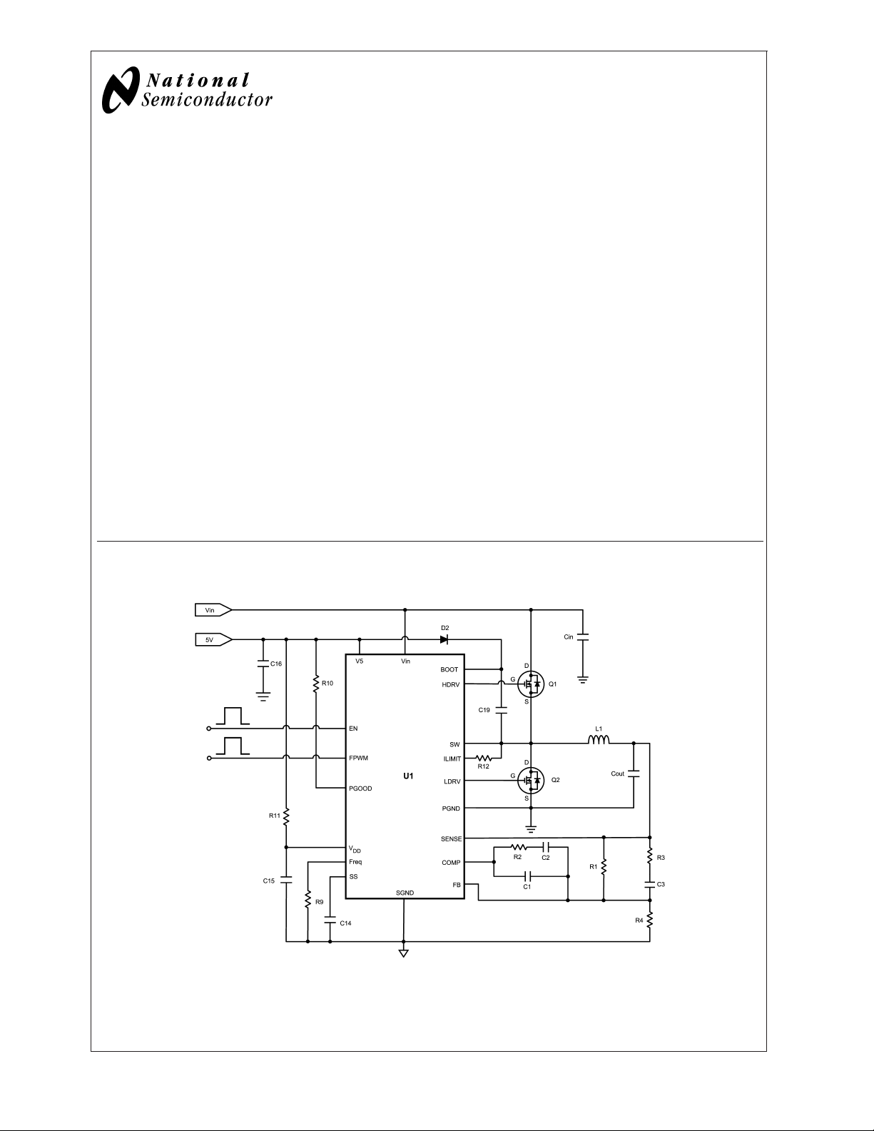
Typical Application
See Figure 17 for Expanded View
Features
n Input voltage range from 5.5V to 28V
n Forced-PWM or Pulse-skip modes
n Lossless bottom-side FET current sensing
n Adaptive duty cycle clamping
n High current N-channel FET drivers
n Low shutdown supply currents
n Reference voltage accurate to within
n Output voltage adjustable down to 0.6V
n Power Good flag and Chip Enable
n Under-voltage lockout
n Over-voltage/Under-voltage protection
n Soft-start and Soft-shutdown
n Switching frequency adjustable 200kHz-500kHz
±
1.5%
Applications
n Notebook Chipset Power Supplies
n Low Output Voltage High Efficiency Buck Regulators
20120104
© 2005 National Semiconductor Corporation DS201201 www.national.com
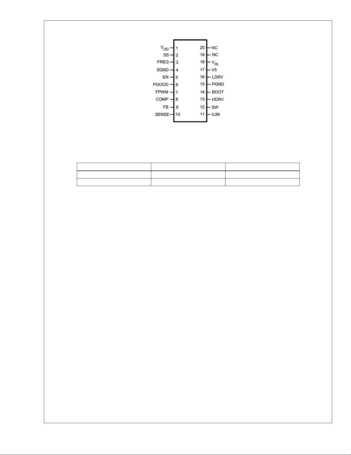
Connection Diagram
LM27241
20-Lead TSSOP (MTC)
Ordering Information
Order Number Package Drawing Supplied As
LM27241MTC MTC20 73 Units/Rail
LM27241MTCX MTC20 2500 Units/13" Reel
Pin Description
Pin 1, VDD: 5V supply rail for the control and logic sections.
For normal operation the voltage on this pin must be brought
above 4.5V. Subsequently, the voltage on this pin (including
any ripple component) should not be allowed to fall below 4V
for a duration longer than 7µs. Since this pin is also the
supply rail for the internal control sections, it should be
well-decoupled particularly at high frequencies. A minimum
0.1µF-0.47µF (ceramic) capacitor should be placed on the
component side very close to the IC with no intervening vias
between this capacitor and the VDD/SGND pins. If the voltage on Pin 1 falls below the lower UVLO threshold, upper
FET(s) are latched OFF and the lower FET(s) are latched
ON. Power Not Good is then signaled immediately (on Pin
6). To initiate recovery, the EN pin must be taken below 0.8V
and then back above 2V (with VDD held above 4.5V). Or the
voltage on the VDD pin must be taken below 1.0V and then
back again above 4.5V (with EN pin held above 2V). Normal
operation will then resume assuming that the fault condition
has been cleared.
Pin 2, SS: Soft-start pin. A Soft-start capacitor is placed
between this pin and ground. A typical capacitance of 0.1µF
is recommended between this pin and ground. The IC connects an internal 1.8 kΩ resistor (R
Characteristics table) between this pin and ground to discharge any remaining charge on the Soft-start capacitor
under several conditions. These conditions include the initial
power-up sequence, start-up by toggling the EN pin, and
also recovery from a fault condition. The purpose is to bring
down the voltage on the Soft-start pin to below 100mV for
obtaining reset. Reset having thus been obtained, an 11µA
current source at this pin charges up the Soft-start capacitor.
The voltage on this pin controls the maximum duty cycle,
and this produces a gradual ramp-up of the output voltage,
thereby preventing large inrush currents into the output capacitors. The voltage on this pin finally clamps close to 5V.
This pin is connected to an internal 115µA current sink
whenever a current limit event is in progress. This sink
SS_DCHG
, see Electrical
Top View
20120102
current discharges the Soft-start capacitor and forces the
duty cycle low to protect the power components. When a
fault condition is asserted (See Pin 9) the SS pin is internally
connected to ground via the 1.8 kΩ resistor.
Pin 3, FREQ: Frequency adjust pin. The switching frequency
is set by a resistor connected between this pin and ground.
A value of 22.1kΩ sets the frequency to 300kHz (nominal). If
the resistance is increased, the switching frequency decreases. An approximate relationship is that for every 7.3kΩ
increase or decrease in the value of the frequency set resistor, the total switching period increases or decreases by 1µs.
Pin 4, SGND: Signal Ground pin. This is the lower rail for the
control and logic sections. SGND should be connected on
the PCB to the system ground, which in turn is connected to
PGND. The layout is important and the recommendations in
the section Layout Guidelines should be followed.
Pin 5, EN: IC Enable pin. When EN is taken high, the output
is enabled by means of a Soft-start power-up sequence.
When EN is brought low, Power Not Good is signaled within
100ns. This causes Soft-shutdown to occur (see Pins 2 and
6). The Soft-start capacitor is then discharged by an internal
1.8kΩ resistor (R
table). When the Enable pin is toggled, a fault condition is
not asserted. Therefore in this case, the lower FET is not
latched ON, even as the output voltage ramps down, eventually falling below the under-voltage threshold. In fact, in
this situation, both the upper and the lower FETs are latched
OFF, until the Enable pin is taken high again. If a fault
shutdown has occurred, taking the Enable pin low and then
high again (toggling), resets the internal latches, and the IC
will resume normal switching operation.
Pin 6, PGOOD: Power Good output pin. An open-drain logic
output that is pulled high with an external pull-up resistor,
indicating that the output voltage is within a pre-defined
Power Good window. Outside this window, the pin is internally pulled low (Power Not Good signaled) provided the
output error lasts for more than 7µs. The pin is also pulled
low within 100ns of the Enable pin being taken low, irrespec-
SS_DCHG
, see Electrical Characteristics
www.national.com 2

Pin Description (Continued)
tive of the output voltage level. PGOOD must always first be
"high" before it can respond to a proper fault "low" condition.
Under fault assertion, the low-side MOSFET is always
latched ON. This will not happen if regulation has not already
been achieved.
Pin 7, FPWM: Logic input for selecting either the Forced
PWM (FPWM) Mode or Pulse-skip Mode (SKIP). When the
pin is driven high, the IC operates in the FPWM mode, and
when pulled low or left floating, the SKIP mode is enabled. In
FPWM mode, the lower FET is always ON whenever the
upper FET is OFF (except for a narrow shoot-through protection deadband). This leads to continuous conduction
mode of operation, which has a fixed frequency and (almost)
fixed duty cycle down to very light loads. But this does
reduce efficiency at light loads. The alternative mode is SKIP
mode. This mode forces the lower MOSFET ON only until
the voltage on the Switch pin is more negative than 2.2mV
(typical). As an example, for a 21mΩ FET, this translates to
a current threshold of 2.2mV/21mΩ = 0.1A. Therefore, if the
(instantaneous) inductor current falls below this value, the
lower FET will turn OFF every cycle at this point (when
operated in SKIP mode). This threshold is set by the zerocross Comparator in the Block Diagram. Note that if the
inductor current is high enough to be always above this
zero-cross threshold (V
tics table), there will be no observable difference between
FPWM and SKIP mode settings (in steady-state). SKIP
mode is clearly a discontinuous mode of operation. However, in conventional discontinuous mode, the duty cycle
keeps falling (towards zero) as the load decreases. But the
LM27241 does not allow the duty cycle to fall by more than
15% of its original value (at the CCM-DCM boundary). This
forces pulse-skipping, and the average frequency is effectively decreased as the load decreases. This mode of operation improves efficiency at light loads, but the frequency is
effectively no longer a constant. Note that a minimum pre-
load of 0.1mA should be maintained on the output to ensure
regulation in SKIP mode. The resistive divider from output to
ground used to set the output voltage could be designed to
serve as part or all of this required pre-load.
Pin 8, COMP: Compensation pin. This is also the output of
the error amplifier. The voltage level on this pin is compared
with an internally generated ramp signal to set the duty cycle
for normal regulation. Since the Feedback pin is the inverting
input of the same error amplifier, appropriate control loop
compensation components are placed between this pin and
the Feedback pin. The COMP pin is internally pulled low
during Soft-start so as to limit the duty cycle. Once Soft-start
is completed, the voltage on this pin can take up the value
required to maintain output regulation. An internal voltage
clamp at this pin forms an adaptive duty cycle clamp feature.
This serves to limit the maximum allowable duty cycles and
peak currents under sudden overloads. But at the same time
it has enough headroom to permit an adequate response to
step loads within the normal operating range.
Pin 9, FB: Feedback pin. This is the inverting input of the
error amplifier. The voltage on this pin under regulation is
nominally at 0.6V. A Power Good window on this pin determines if the output voltage is within regulation limits (
If the voltage falls outside this window for more than 7µs,
Power Not Good is signaled on the PGOOD pin (Pin 6).
Output over-voltage and under-voltage conditions are also
detected by comparing the voltage on the Feedback pin with
appropriate internal reference voltage levels. If the voltage
exceeds the safe window (
SW_ZERO
, see Electrical Characteris-
±
13%).
±
30%) for longer than 7µs, a fault
condition is asserted. Then lower FET is latched ON and the
upper FET is latched OFF.
Pin 10, SENSE: Output voltage sense pin. It is tied directly
to the output rail. The SENSE pin voltage is used together
with the VIN voltage (on Pin 18) to (internally) calculate the
CCM (continuous conduction mode) duty cycle. This calculation is used by the IC to set the minimum duty cycle in the
SKIP mode to 85% of the CCM value. It is also used to set
the adaptive duty cycle clamp. An internal 20Ω resistor from
the SENSE pin to ground discharges the output capacitor
gently (Soft-shutdown) whenever Power Not Good is signaled on Pin 6.
Pin 11, ILIM: Current Limit pin. When the bottom FET is ON,
a 62µA (typical) current flows out of the ILIM pin and into an
external resistor that is connected to the drain of the lower
MOSFET. This current through the resistor creates a voltage
on the ILIM pin. However, the drain voltage of the lower
MOSFET will go more negative as the load current is increased through the R
of instantaneous current, the voltage on this pin will transit
from positive to negative. The point where it is zero is the
current limiting condition and is detected by the Current Limit
Comparator. When a current limit condition has been detected, the next ON-pulse of the upper FET will be omitted.
The lower FET will again be monitored to determine if the
current has fallen below the threshold. If it has, the next
ON-pulse will be permitted. If not, the upper FET will be
turned OFF and will stay so for several cycles if necessary,
until the current returns to normal. Eventually, if the overcurrent condition persists, and the upper FET has not been
turned ON, the output will clearly start to fall. Ultimately the
output will fall below the under-voltage threshold, and a fault
condition will be asserted by the IC.
Pin 12, SW: The Switching node of the buck regulator. Also
serves as the lower rail of the floating driver of the upper
FET.
Pin 13, HDRV: Gate drive pin for the upper FET. The top
gate driver is interlocked with the bottom gate driver to
prevent shoot-through/cross-conduction.
Pin 14, BOOT: Bootstrap pin. This is the upper supply rail for
the floating driver of the upper FET. It is bootstrapped by
means of a ceramic capacitor connected to the channel
Switching node. This capacitor is charged up by the IC to a
value of about 5V as derived from the V5 pin (Pin 17).
Pin 15, PGND: Power Ground pin. This is the return path for
the bottom FET gate drive. The PGND is to be connected on
the PCB to the system ground and also to the Signal ground
(Pin 4) in accordance with the recommended Layout Guidelines .
Pin 16, LDRV: Gate drive pin for the bottom FET (Low-side
drive). The bottom gate driver is interlocked with the top gate
driver to prevent shoot-through/cross-conduction. It is always latched high when a fault condition is asserted by the
IC.
Pin 17, V5: Upper rail of the lower FET driver. Also used to
charge up the bootstrap capacitor of the upper FET driver.
This is connected to an external 5V supply. The 5V rail may
be the same as the rail used to provide power to the VDD pin
(Pin 1), but the VDD pin will then require to be welldecoupled so that it does not interact with the V5 pin. A
low-pass RC filter consisting of a ceramic 0.1µF capacitor
(preferably 0.22µF) and a 10Ω resistor will suffice as shown
in the Typical Applications circuit.
Pin 18, VIN: The input to the Buck regulator power stage. It
is also used by the internal ramp generator to implement the
of the MOSFET. At some value
DS_ON
LM27241
www.national.com3

Pin Description (Continued)
line feedforward feature. The VIN pin is also used with the
LM27241
SENSE pin voltage to predict the CCM (continuous conduction mode) duty cycle and to thereby set the minimum al-
lowed DCM duty cycle to 85% of the CCM value. This is a
high input impedance pin, drawing only about 100µA (typical) from the input rail.
Pin 19, 20 NC: No Connect.
www.national.com 4
LM27241
Absolute Maximum Ratings (Note 1)
If Military/Aerospace specified devices are required,
please contact the National Semiconductor Sales Office/
Distributors for availability and specifications.
Voltages from the indicated pins to SGND/PGND unless
otherwise indicated (Note 2):
VIN -0.3V to 30V
V5 -0.3V to 7V
VDD -0.3V to 7V
Junction Temperature +150˚C
ESD Rating (Note 4) 2kV
Ambient Storage Temperature
Range -65˚C to +150˚C
Soldering Dwell Time,
Temperature
Wave
Infrared
Vapor Phase
4 sec, 260˚C
10 sec, 240˚C
75 sec, 219˚C
BOOT -0.3V to 36V
BOOT to SW -0.3V to 7V
SW -0.3V to 30V
ILIM -0.3V to 30V
SENSE, FB -0.3V to 7V
Operating Ratings (Note 1)
VIN 5.5V to 28V
VDD, V5 4.5V to 5.5V
Junction Temperature -5˚C to +125˚C
PGOOD -0.3V to 7V
EN -0.3V to 7V
Power Dissipation (T
= 25˚C)
A
(Note 3) 0.75W
Electrical Characteristics
Specifications with standard typeface are for TJ= 25˚C, and those with boldface apply over full Operating Junction Temperature range. VDD = V5 = 5V, V
SGND=VPGND
= 0V, VIN = 15V, VEN= 3V, R
Datasheet min/max specification limits are guaranteed by design, test, or statistical analysis.
Symbol Parameter Conditions Min
Reference
V
FB_REG
V
FB_LINE REG
FB Pin Voltage at
Regualtion
VFBLine Regulation VDD = 4.5V to 5.5V,
VDD = 4.5V to 5.5V,
VIN = 5.5V to 28V
VIN = 5.5V to 28V
I
FB
FB Pin Current (sourcing) VFBat regulation 20 100 nA
Chip Supply
I
Q_VIN
I
SD_VIN
I
Q_VDD
I
SD_VDD
I
Q_V5
I
SD_V5
I
Q_BOOT
I
SD_BOOT
V
DD_UVLO
HYS
VDD_UVLO
VIN Quiescent Current VFB= 0.7V 100 200 µA
VIN Shutdown Current VEN=0V 0 5 µA
VDD Quiescent Current VFB= 0.7V 1.75 3 mA
VDD Shutdown Current VEN=0V 8 15 µA
V5 Normal Operating
Current
VFB= 0.7V 0.3 0.5 mA
V
= 0.5V 0.5 1.25
FB
V5 Shutdown Current VEN=0V 0 5 µA
BOOT Quiescent Current VFB= 0.7V 2 5 µA
V
= 0.5V 300 500
FB
BOOT Shutdown Current VEN=0V 1 5 µA
VDD UVLO Threshold VDD rising from 0V 3.9 4.2 4.5 V
VDD UVLO Hysteresis VDD = V5 falling from
V
DD_UVLO
Logic
I
EN
V
EN_HI
V
EN_LO
R
FPWM
V
FPWM_HI
V
FPWM_LO
EN Input Current VEN=0to5V 0 µA
EN Input Logic High 2 1.8 V
EN Input Logic Low 1.3 0.8 V
FPWM Pull-down V
=2V 100 200 1000 kΩ
FPWM
FPWM Input Logic High 2 1.8 V
FPWM Input Logic Low 1.3 0.8 V
= 22.1K unless otherwise stated (Note 5).
FADJ
Typical
(Note 7)
Max Units
591 600 609 mV
0.5
0.5 0.7 0.9 V
www.national.com5
Electrical Characteristics (Continued)
Specifications with standard typeface are for TJ= 25˚C, and those with boldface apply over full Operating Junction Tempera-
LM27241
ture range. VDD = V5 = 5V, V
SGND=VPGND
Datasheet min/max specification limits are guaranteed by design, test, or statistical analysis.
Symbol Parameter Conditions Min
Power Good
V
PGOOD_HI
Power Good Upper
Threshold as a Percentage
of Internal Reference
V
PGOOD_LOW
Power Good Lower
Threshold as a Percentage
of Internal Reference
HYS
PGOOD
∆t
PG_OK
∆t
PG_NOK
∆t
SD
V
PGND_SAT
I
PGOOD_LEAK
Power Good Hysteresis 7 %
Power Good Delay From output voltage “good”
PGOOD Saturation Voltage PGOOD de-asserted (Power
PGOOD Leakage Current PGOOD = 5V and asserted 0 1 µA
OV and UV Protection
V
OVP_RISING
Fault OVP Latch Threshold
as a Percentage of Internal
Reference
V
OVP_FALLING
Fault UVP Latch Threshold
as a Percentage of Internal
Reference
∆t
FAULT
Fault Delay From Fault detection (any
Soft-start
I
SS_CHG
R
SS_DCHG
Soft-start Charging Current VSS=1V 8 11 14 µA
Soft-shutdown Resistance
(SS pin to SGND)
I
SS_DCHG
Soft-start Discharge
Current
V
SS_RESET
Soft-start pin reset voltage
(Note 6)
V
OS
SS to COMP Offset
Voltage
Error Amplifier
GAIN DC Gain 70 dB
V
SLEW
Voltage Slew Rate COMP rising 4.45 V/µs
BW Unity Gain Bandwidth 6.5 MHz
I
COMP_SOURCE
I
COMP_SINK
COMP Source Current V
COMP Sink Current V
Current Limit and Zero-Cross
= 0V, VIN = 15V, VEN= 3V, R
FB voltage rising above
V
FB_REG
FB voltage falling below
V
FB_REG
to PGOOD assertion.
From the output voltage
“bad” to PGOOD
de-assertion
From Enable low to PGOOD
low
Not Good) and sinking
1.5mA
FB voltage rising above
V
FB_REG
FB voltage falling below
V
FB_REG
output) to Fault assertion
VEN= 0V, VSS= 1V 1800 Ω
In Current Limit 80 115 160 µA
SS charged to 0.5V, EN low
to high
VSS= 0.5V and 1V, VFB=
0V
COMP falling 2.25
<
V
FB
FB_REG
V
= 0.5V
COMP
>
V
FB
FB_REG
V
= 0.5V
COMP
= 22.1K unless otherwise stated (Note 5).
FADJ
Typical
(Note 7)
Max Units
110 113 116 %
84 87 90 %
10 20 30 µs
4 7 10
0.03 0.1
0.12 0.4 V
125 130 135 %
65 70 75 %
7µs
100 mV
600 mV
2 5mA
7 14 mA
www.national.com 6
Electrical Characteristics (Continued)
Specifications with standard typeface are for TJ= 25˚C, and those with boldface apply over full Operating Junction Temperature range. VDD = V5 = 5V, V
SGND=VPGND
= 0V, VIN = 15V, VEN= 3V, R
Datasheet min/max specification limits are guaranteed by design, test, or statistical analysis.
Symbol Parameter Conditions Min
I
ILIM
V
ILIM_TH
V
SW_ZERO
ILIM Pin Current (sourcing) V
I
Threshold Voltage -10 0 10 mV
ILIM
Zero-cross Threshold (SW
=0V 46 62 76 µA
ILIM
LDRV goes low -2.2 mV
Pin)
Oscillator
F
OSC
V
RAMP
V
VALLEY
∆F
OSC_VIN
PWM Frequency R
PWM Ramp Peak-to-peak
Amplitude
= 22.1kΩ 255 300 345 kHz
FADJ
R
= 12.4kΩ 500
FADJ
R
= 30.9kΩ 200
FADJ
VIN = 15V 1.6 V
VIN = 24V 2.95
PWM Ramp Valley 0.8 V
Frequency Change with
VIN = 5.5V to 24V
VIN
∆F
OSC_VDD
Frequency Change with
VDD = 4.5V to 5.5V
VDD
V
FREQ_VIN
FREQ Pin Voltage vs. VIN 0.105 V/V
System
t
ON_MIN
D
MAX
Minimum ON Time V
=3V 30 ns
FPWM
Maximum Duty Cycle VIN = 5.5V 60 75 %
VIN = 15V 40 50 %
VIN = 28V, VDD= 4.5V 22 28 %
Gate Drivers
R
HDRV_SOURCE
HDRV Source Impedance HDRV Pin Current
(sourcing)= 1.2A
R
HDRV_SINK
HDRV Sink Impedance HDRV Pin Current (sinking)
=1A
R
LDRV_SOURCE
LDRV Source Impedance LDRV Pin Current (sourcing)
= 1.2A
R
LDRV_SINK
LDRV Sink Impedance LDRV Pin Current (sinking)
=2A
t
DEAD
Cross-conduction
Protection Delay
(deadtime)
HDRV Falling to LDRV
Rising
LDRV Falling to HDRV
Rising
= 22.1K unless otherwise stated (Note 5).
FADJ
Typical
(Note 7)
±
1%
±
2%
Max Units
7 Ω
2 Ω
7 Ω
1 Ω
40 ns
70
LM27241
Note 1: Absolute maximum ratings indicate limits beyond which damage to the device may occur. Operating Ratings are conditions under which operation of the
device is guaranteed. For guaranteed performance limits and associated test conditions, see the Electrical Characteristics table.
Note 2: PGND and SGND are all electrically connected together on the PCB.
Note 3: The maximum allowable power dissipation is calculated by using P
ambient temperature, and θ
from using 125˚C, 25˚C, and 118˚C/W for T
TSSOP package. The θ
ambient temperatures. For detailed information on soldering plastic TSSOP package, refer to http://www.national.com/packaging/.
Note 4: ESD is applied by the human body model, which is a 100pF capacitor discharged through a 1.5 kΩ resistor into each pin.
Note 5: R
Note 6: If the LM27241 starts up with a pre-charged soft start capacitor, it will first discharge the capacitor to V
process.
Note 7: Typical numbers are at 25˚C and represent the most likely norm.
is the frequency adjust resistor between FREQ pin and Ground.
FADJ
is the junction-to-ambient thermal resistance of the specified package. The 0.75W rating of the TSSOP-20 package for example results
JA
value above represents the worst-case condition with no heat sinking. Heat sinking will permit more power to be dissipated at higher
JA
, and θJArespectively. The rated power dissipation should be derated by 10mW/˚C above 25˚C ambient for the
JMAX,TA
Dmax
=(T
JMAX-TA
)/θJA, where T
is the maximum junction temperature, TAis the
JMAX
SS_RESET
and then begin the normal Soft-start
www.national.com7
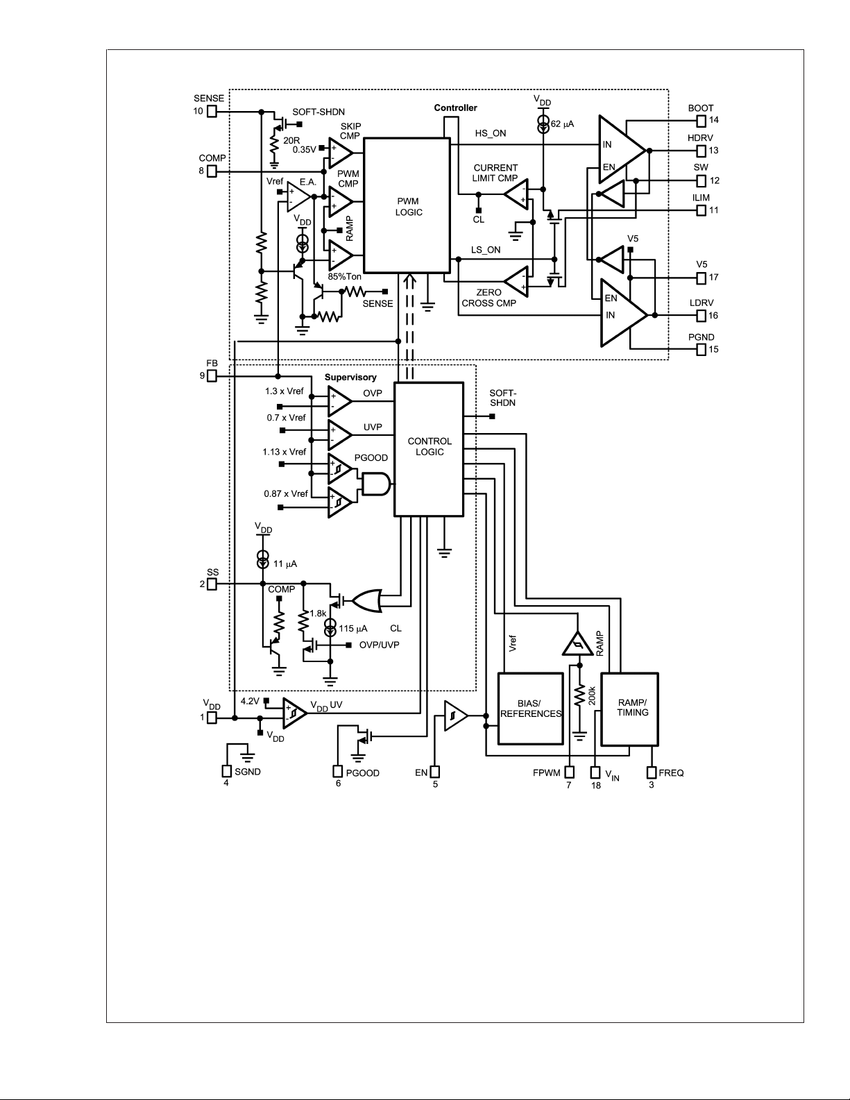
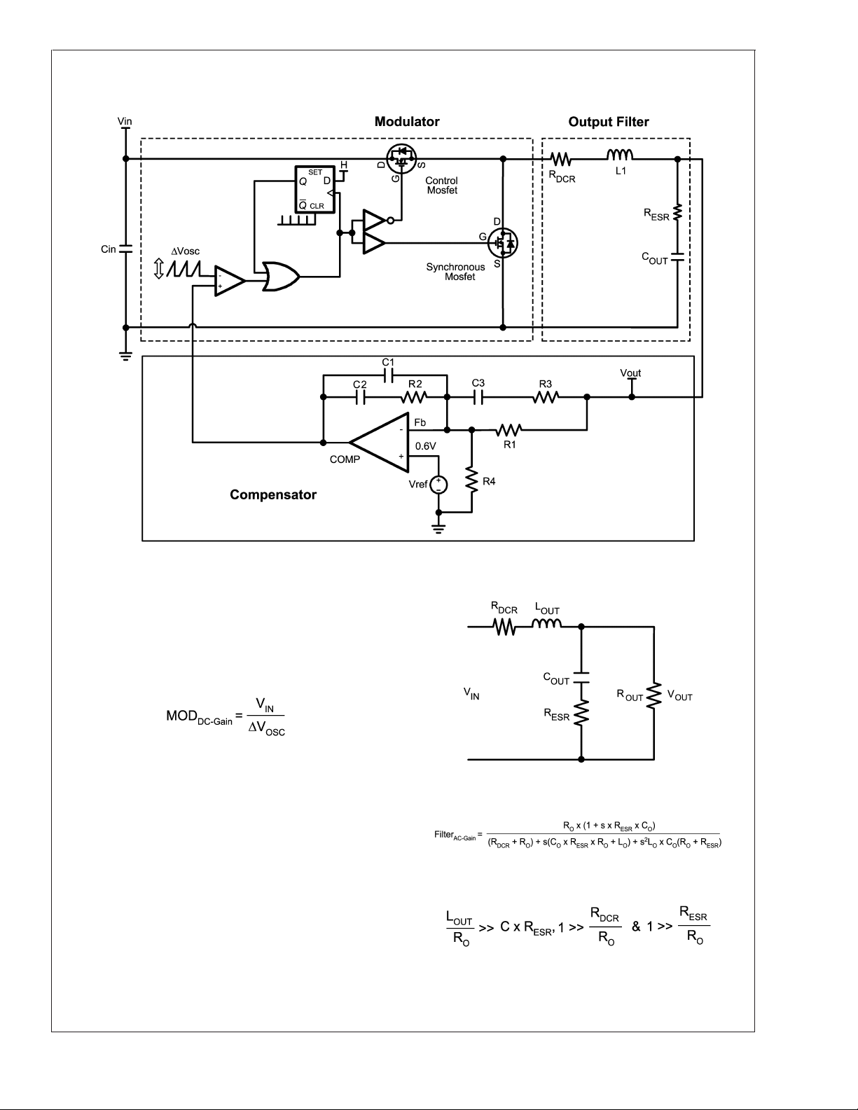
Block Diagram
LM27241
www.national.com 8
20120101
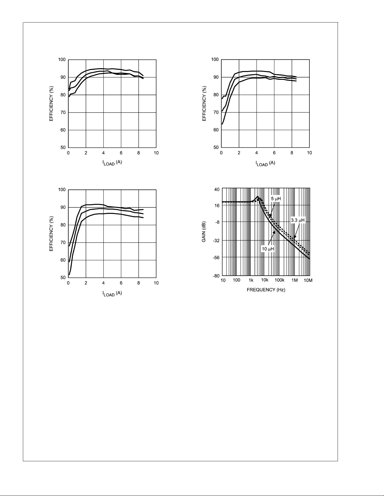
Typical Performance Characteristics Input Voltage is 12V, 18V, 24V (in order) starting from upper-
most curve to lowermost curve in each of the Efficiency plots below.
Efficiency for 2.5V Output Efficiency for 1.5V Output
LM27241
20120105
Efficiency for 1.05V Output Modulator (Plant) Gain
20120107
20120106
20120108
www.national.com9

Operation Descriptions
GENERAL
LM27241
The LM27241 is a synchronous buck controller using a
voltage-mode control topology. This topology was selected
to provide fixed-frequency PWM regulation at very low duty
cycles, in preference to current-mode control, because the
latter has inherent limitations in being able to achieve low
pulse widths due to blanking time requirements. Because of
a minimum pulse width of about 30ns for the LM27241, very
low duty cycles (low output, high input) are possible. The
main advantage of current-mode control is the fact that the
slope of its ramp (derived from the switch current), automatically increases with increase in input voltage. This leads to
improved line rejection and fast response to line variations.
In typical voltage-mode control, the ramp is derived from the
clock, not from the switch current. But by using the input
voltage together with the clock signal to generate the ramp
as in the LM27241, this advantage of current-mode control
can in fact be completely replicated. The technique is called
line feedforward. In addition, the LM27241 features a userselectable Pulse-skip mode that significantly improves efficiency at light loads by reducing switching losses, and driver
consumption, both of which are proportional to switching
frequency.
INPUT VOLTAGE FEEDFORWARD
The feedforward circuit of the LM27241 adjusts the slope of
the internal PWM ramp in proportion to the regulator input
voltage. See Figure 1 for an illustration of how the duty cycle
changes as a result of the change in the slope of the ramp,
even though the error amplifier output has not had time to
react to the line disturbance. The almost instantaneous duty
cycle correction provided by the feedforward circuit significantly improves line transient rejection.
20120109
FIGURE 1. Voltage Feedforward
FORCED-PWM MODE AND PULSE-SKIP MODE
Forced-PWM mode (FPWM) leads to Continuous Conduction Mode (CCM) even at very light loads. It is one of two
user-selectable modes of operation provided by the
LM27241. When FPWM is chosen (FPWM pin high), the
bottom FET will always be turned ON whenever the top FET
is OFF. See Figure 2 for a typical FPWM plot.
www.national.com 10
CH1: HDRV, CH2: LDRV, CH3: SW, CH4: IL(0.2A/div)
@
Output 1V
0.04A, VIN = 10V, FPWM, L = 10µH, f = 300kHz
FIGURE 2. Normal FPWM Mode Operation at Light
Loads
20120110

Operation Descriptions (Continued)
In a conventional converter, as the load is decreased to
about 10% - 30% of maximum load current, DCM (Discontinuous Conduction Mode) occurs. In this condition the inductor current falls to zero during the OFF-time, and stays
there until the start of the next switching cycle. In this mode,
if the load is decreased further, the duty cycle decreases
(pinches off), and ultimately may decrease to the point
where the required pulse width becomes less than the minimum ON-time achievable by the converter (controller +
FETs). Then a sort of random skipping behavior occurs as
the error amplifier struggles to maintain regulation. This is
not the most desirable type of behavior. There are two
modes of operation that address this issue.
The first method is to keep the lower FET ON until the start
of the next cycle (as in the LM27241 operated in FPWM
mode). This allows the inductor current to drop to zero and
then actually reverse direction (negative direction through
inductor, passing from Drain to Source of lower FET, see
Channel 4 in Figure 2). Now the current can continue to flow
continuously till the end of the switching cycle. This maintains CCM and therefore the duty cycle does not start to
pinch off as in typical DCM. Nor does it lead to the undesirable random skipping described above. Note that the pulse
width (duty cycle) for CCM is virtually constant for any load
and therefore does not usually run into the minimum ONtime restriction. The LM27241 can exhibit skip pulsing in
FPWM when the Duty-Cycle is very low, and the switching
frequency is high (minimum ON-Time). Let us check the
LM27241 to rule out this remote possibility. For example,
with an input of 24V, an output of 1V, the duty cycle is 1/24 =
4.2%. This leads to a required ON-time of 0.042* 3.3 = 0.14
µs at a switching frequency of 300kHz (T=3.3 µs). Since
140ns exceeds the minimum ON-time of 30ns of the
LM27241, normal constant frequency CCM mode of operation is assured in FPWM mode, at virtually any load.
Another way out of the problematic spontaneous DCM operation is the second operating mode of the LM27241, the
Pulse-skip (SKIP) Mode. In SKIP Mode, a zero-cross detector at the SW pin turns off the bottom FET when the inductor
current decays to zero (actually at V
SW_ZERO
Characteristics table). This would however still amount to
conventional DCM, with its associated problems at extremely light loads as described earlier. The LM27241 however avoids the random skipping behavior described earlier,
and replaces it with a more defined or formal SKIP mode. In
conventional DCM, a converter would try to reduce its duty
cycle from the CCM value as the load decreases, as explained previously. So it would start with the CCM duty cycle
value (at the CCM-DCM boundary), but as the load decreases, the duty cycle would try to shrink to zero. However,
in the LM27241, the DCM duty cycle is not allowed to fall
below 85% of the CCM value. So when the theoretically
required DCM duty cycle value falls below what the
LM27241 is allowed to deliver (in this mode), pulse-skipping
starts. It will be seen that several of these excess pulses may
be delivered, until the output capacitors charge up enough to
notify the error amplifier and cause its output to reverse.
Thereafter several pulses could be skipped entirely until the
output of the error amplifier again reverses. The SKIP mode
leads to a reduction in the average switching frequency.
Switching losses and FET driver losses, both of which are
proportional to switching frequency, are significantly reduced
at very light loads and efficiency is boosted. SKIP mode also
reduces the circulating currents and energy associated with
, see Electrical
the FPWM mode. See Figure 3 for a typical plot of SKIP
mode at very light loads. Note the bunching of several
fixed-width pulses followed by skipped pulses. The average
frequency can actually fall very low at very light loads. Note
however that when this happens the inductor core is seeing
only very mild flux excursions, and so no significant audible
noise is created. If EMI is a particularly sensitive issue for the
particular application, the user can simply opt for the slightly
less efficient, though constant frequency FPWM mode.
CH1: HDRV, CH2: LDRV, CH3: SW, CH4: IL(0.2A/div)
@
Output 1V
0.04A, VIN = 10V, SKIP, L = 10µH, f = 300kHz
20120111
FIGURE 3. Normal SKIP Mode Operation at Light
Loads
The SKIP mode is enabled when the FPWM pin is held low
(or left floating). Note that at higher loads, and under steady
state conditions (above CCM-DCM boundary), there will be
absolutely no difference in the behavior of the LM27241 or
the associated converter waveforms based on the voltage
applied on the FPWM pin. The differences show up only at
light loads.
Under startup, the peak current through the inductor is
higher than the steady state peak current. This is due to the
output capacitors being charged up to the regulated output
voltage. There will be no observable difference in the shape
of the ramp-up of the output rails in either SKIP mode or
FPWM mode. The design has thus forced the startup waveforms to be identical irrespective of whether the FPWM
mode or the SKIP mode has been selected.
The designer must realize that even at zero load condition,
there is circulating current when operating in FPWM mode.
This is illustrated in Figure 4. Duty cycle remains fairly constant in CCM, thereforeV=Lx∆I/∆t . It can be seen that I
in Figure 4) must remain constant for any load,
(or I
pp
including zero load current. At zero load, the average current
through the inductor is zero, so the geometric center of the
sawtooth waveform (the center being always equal to load
current) is along the x-axis. At critical conduction (boundary
between conventional CCM and what should have been
DCM were it not in FPWM mode), the load current is equal to
Ipp/2. Note that excessively low values of inductance will
produce much higher current ripple and this will lead to
higher circulating currents and power dissipation.
LM27241
www.national.com11

Operation Descriptions (Continued)
LM27241
inductor could also saturate severely at this point if designed
for light loads. In general, if the designer wants to toggle the
FPWM pin while the converter is operating or if FPWM mode
is required for a light load application, the low side FET and
inductor should be closely evaluated under this specific condition. If the part is operated in FPWM mode with a light load
the user will experience lower efficiency and negative current
during the transition (as discussed). The user may also
experience a momentary drop on Vout when the transition is
made from SKIP to FPWM mode. This only occurs for no
load or very light load conditions (above the DCM boundary
there is no difference between SKIP FPWM modes).
<
In some cases, such as low Vout (
1.5V), a glitch may be
present on PGOOD. If this is problematic, the glitch may be
eliminated by either operating in SKIP mode or using a small
sized soft start capacitor. See the following section for selecting soft start capacitors .
20120112
FIGURE 4. Inductor Current in FPWM Mode
STATE-TRANSITIONS AT LIGHT LOADS
A situation can occur if the converter transitions from SKIP
mode to FPWM mode under a light load condition (converter
is operating below the DCM boundary). This can occur after
startup if FPWM mode is selected for use in a light load
condition or if the FPWM pin is toggled high during normal
operation at light load. The problem occurs because in SKIP
mode the converter is operating at a set duty cycle and a
lower average frequency. When the converter is forced into
FPWM mode, this represents a change to the system. The
pulse widths and frequencies need to re-adjust suddenly and
in the process momentary imbalances can be created. Like
the case of a pre-biased load, there can be negative surge
current passing from drain to source of the lower FET. It must
be kept in mind that though the LM27241 has current limiting
for current passing in the ‘positive’ direction (i.e. passing
from source to drain of the lower FET), there is no limit for
reverse currents. The amount of reverse current when the
FPWM pin is toggled ‘on the fly’ can be very high. This
current is determined by several factors. One key factor is
the output capacitance. Large output capacitances will lead
to higher peak reverse currents. The reverse swing will be
higher for lighter loads because of the bigger difference
between the duty cycles/average frequency in the two
modes. See Figure 5 for a plot of what happened in going
from SKIP to FPWM mode at 0A load (worst case). The peak
reverse current was as high as 3A, lasting about 0.1ms. The
CH1: PGOOD, CH2: Vo, CH3: LDRV, CH4: IL(1A/div)
@
Output 1V
0A, VIN = 10V, L = 10µH, f = 300kHz
20120113
FIGURE 5. SKIP to FPWM ’On The Fly’
SOFT-START
The maximum output voltage of the error amplifier is limited
during start-up by the voltage on the 0.1µF capacitor connected between the SS pin and ground. When the controller
is enabled (by taking EN pin high) the following steps may
occur. First the SS capacitor is discharged (if it has a precharge) by a 1.8 kΩ internal resistor (R
SS_DCHG
, see Electrical Characteristics table). This ensures that reset is obtained. Then a charging current source I
SS_CHG
of 11µA is
applied at this pin to bring up the voltage of the Soft-start
capacitor voltage gradually. This causes the (maximum allowable) duty cycle to increase slowly, thereby limiting the
charging current into the output capacitor and also ensuring
that the inductor does not saturate. The Soft-start capacitor
will eventually charge up close to the 5V input rail. When EN
is pulled low the Soft-start capacitor is discharged by the
same 1.8 kΩ internal resistor and the controller is shutdown.
Now the sequence is allowed to repeat the next time EN is
taken high.
The above Soft-start sequence is actually initiated not only
whenever EN is taken high, but also under a normal
power-up or during recovery from a fault condition (more on
this later).
www.national.com 12

Operation Descriptions (Continued)
As mentioned in the section ‘Forced-PWM Mode and Pulseskip Mode’ under startup, since the current is high until the
output capacitors have charged up, there will be no observable difference in the shape of the ramp-up of the output rail
in either SKIP mode or FPWM mode. The design has thus
forced the startup waveforms to be identical irrespective of
whether the FPWM mode or the SKIP mode has been
selected.
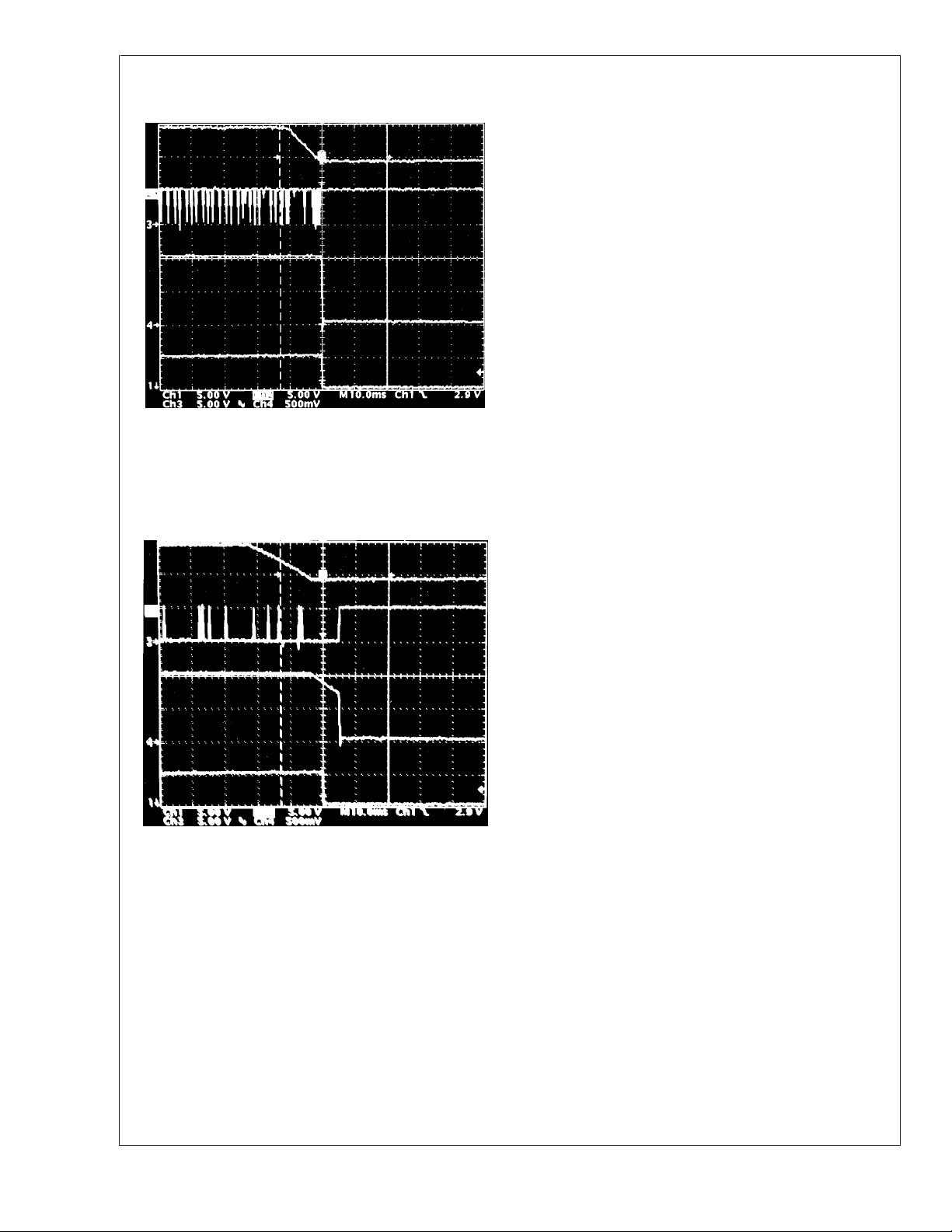
SHUTDOWN/SOFT-SHUTDOWN
When the EN pin is driven low, the LM27241 initiates shutdown by turning OFF both upper and lower FETs completely
(this occurs irrespective of FPWM or SKIP modes). See
Figure 6 for a typical shutdown plot and note that the LDRV
goes to zero (and stays there). Though not displayed, Power
Good also goes low within less than 100ns of the EN pin
going low (t
fore in this case, the controller is NOT waiting for the output
to actually fall out of the Power Good window before it
signals Power Not Good. When the part is shutdown with a
constant current load, the time taken for the output to decay
may be calculated using the equation V/t = i/C. For example,
there is a constant current 2A load applied at the output and
the charge stored on the output capacitor continues to discharge into the load. From V/t = i/C = 2A/330µF, it can be
seen that the output voltage (say 1V) will fall to zero in about
165µs.
, see Electrical Characteristics table). There-
SD
fallen out of the Power Good window (see ∆t
PG_NOK
Electrical Characteristics table). With the feedback pin voltage rising towards regulation value, there is a 20µs delay
between the output being in regulation and the signaling of
Power Good (see ∆t
in Electrical Characteristics
PG_OK
table). Power Not Good is signaled within 100ns of the
Enable pin being pulled low (see ∆t
in Electrical Charac-
SD
teristics table), irrespective of the fact that the output could
still be in regulation. The Soft-start capacitor is also then
discharged as explained earlier.
20120191
FIGURE 7. Startup Power OK
LM27241
in
CH1: LDRV, CH2: Vo, CH3: SW, CH4: IL(1A/div)
@
Output 1V
330µF
2A, VIN = 10V, FPWM/SKIP, L = 10µH, f = 300kHz, C
20120114
OUT
=
FIGURE 6. Shutdown
POWER GOOD/NOT GOOD SIGNALING
PGOOD is an open-drain output pin with an external pull-up
resistor connected to 5V. It goes high (non-conducting) when
the output is within the regulation band as determined by the
Power Good window detector stage on the feedback pin
(see Block Diagram). PGOOD goes low (conducting) when
the output falls out of this window. This signal is referred to
as Power Not Good here. A glitch filter of 7µs filters out
noise, and helps to prevent spurious PGOOD responses. So
Power Not Good is not asserted until 7µs after the output has
FAULT AND RECOVERY
If the output falls outside the Power Good window, the
response is a ‘Power Not Good’ signal. The FET drive signals are not affected. But under a fault condition assertion,
LDRV goes high immediately turning the low-side FET ON
and discharging the output capacitors. The inductor current
will then invariably slew momentarily negative (passing from
drain to source of low-side FET), before it settles down to
zero. A fault will be detected when the output falls below the
Under-voltage threshold, or rises above the Over-voltage
threshold. From its detection to assertion, there is a 7µs
delay to help to prevent spurious responses. A fault condition
is also asserted during a loss of the VIN rail or the VDD rail.
If the Enable pin is brought low prior to this fault, a soft
shutdown will occur. To recover from a fault, either of the
following options is available:
1) Enable pin is toggled: i.e. taken low (below 0.8V), then
high again (2V to 5V). This must be done with VDD between
4.5V to 5V and VIN within normal range (5.5V to 28V).
2) VDD is brought below 1.0V and then brought back up
between 4.5V to 5V. This must be done with the Enable pin
held high (2V to 5V) and VIN within normal range (5.5V to
28V).
Recovery will initiate a Soft-start sequence (see description
under section ‘Soft-start’ above).
VIN POWER-OFF (UVLO)
The LM27241 has an internal comparator that monitors VIN.
If VIN falls to approximately 4.4V, switching ceases and both
top and bottom FETs are turned OFF. ‘Power Not Good’ has
meanwhile already been signaled and a fault condition asserted shortly thereafter.
www.national.com13
Operation Descriptions (Continued)
LM27241
CH1: PGOOD, CH2: VIN, CH3: LDRV, CH4: Vo
@
Output 1V
660µF
0.02A, VIN = 9.75V, FPWM, L = 10µH, f = 300kHz, C
FIGURE 8. VIN Removal in FPWM Mode
20120115
OUT
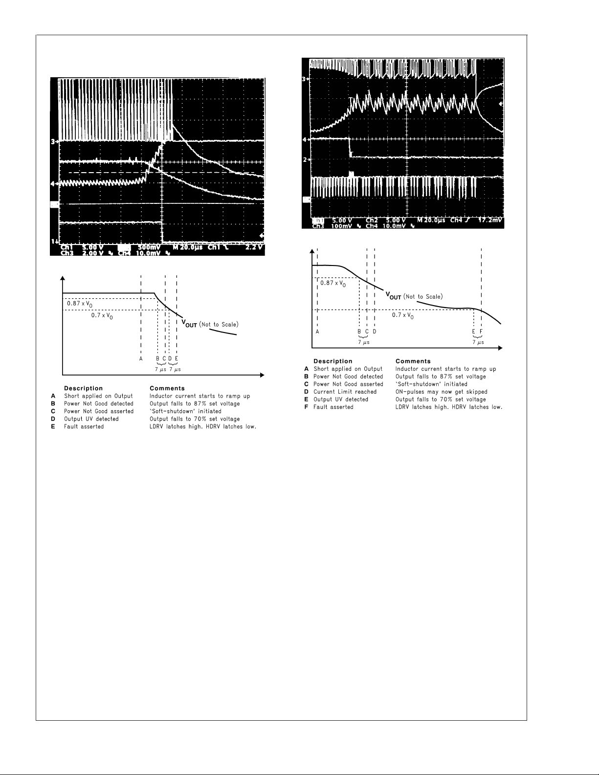
OVER-VOLTAGE PROTECTION
If the voltage on the FB pin exceeds 113% of 0.60V, a Power
Not Good signal is asserted. If the voltage on the FB pin
exceeds 130% of 0.60V, a fault condition is declared, and the
LDRV goes high. If the fault persists, the low-side FET will
stay on and the high-side FET will not turn back on until the
FB pin falls within the power good window, and the Enable
pin is toggled.
CURRENT LIMIT AND PROTECTION
Output current limiting is achieved by sensing the negative
Vds drop across the low-side FET when the FET is turned
ON. The Current Limit Comparator (see Block Diagram)
monitors the voltage at the ILIM pin with 62µA (typical value)
of current being sourced from the pin. The 62µA source flows
through an external resistor connected between ILIM and
the drain of the low-side FET. The voltage drop across the
ILIM resistor is compared with the drop across the low-side
FET and the current limit comparator trips when the two are
of the same magnitude. This determines the threshold of
current limiting. For example, if excessive inductor current
causes the voltage across the low-side FET to exceed the
voltage drop across the ILIM resistor, the ILIM pin will go
=
negative (with respect to ground) and trip the comparator.
The comparator then sets a latch that prevents the high-side
FET from turning ON during the next PWM clock cycle. The
high-side FET will resume switching only if the current limit
comparator was not tripped in the previous switching cycle.
Additionally, the Soft-start capacitor at the SS pin is discharged with a 115µA current source when an overcurrent
event is in progress. The purpose of discharging the Softstart capacitor during an overcurrent event is to eventually
allow the voltage on the SS pin to fall low enough to cause
additional duty cycle limiting.
=(R
R
LIMIT
DS_ONxILIMIT
/62µA)
OUT
20120116
=
CH1: PGOOD, CH2: VIN, CH3: LDRV, CH4: Vo
@
Output 1V
660µF
0.02A, VIN = 9.75V, SKIP, L = 10µH, f = 300kHz, C
FIGURE 9. VIN Removal in SKIP Mode
The recovery procedure from a VIN Power-off is the same as
for any fault condition.
VDD POWER-OFF (UVLO)
Whenever VDD starts to fall, and drops below about 3.5V,
LDRV goes high immediately, ‘Power Not Good’ is signaled
and in effect a fault condition (in this case an Under-voltage
lockout) is asserted. Recovery from a fault is discussed in
the "Fault and Recovery" section.
www.national.com 14
Operation Descriptions (Continued)
LM27241
20120118
20120117
CH1: PGOOD, CH2: Vo, CH3: ILIM Pin, CH4: IL(1A/div)
20120160
Output 1V, 0.04A to Overload, VIN = 10V, FPWM, L = 10µH, f = 300kHz,
RLIM = 1k
FIGURE 10. Response to Severe Overload (Type A:
fault threshold first)
CH1: LDRV, CH2: PGOOD, CH3: ILIM Pin, CH4: IL(5A/div)
20120161
Output 1V, 2A to Overload, VIN = 10V, L = 10µH, f = 300kHz, RLIM = 2k
FIGURE 11. Response to Severe Overload (Type B:
current limit threshold first)
www.national.com15

Application Information
CURRENT LIMIT RESISTOR
LM27241
The timing scheme implemented in the LM27241 makes it
possible for the IC to continue monitoring an over current
condition and to respond appropriately every cycle. This is
explained as follows.
Consider the LM27241 working under normal conditions, just
before an overload occurs. After the end of a given ON-pulse
(say ‘ton1’), the LM27241 starts sampling the current in the
low-side FET. This is the OFF-duration called ‘toff1’ in this
analysis. Therefore, if an over-current condition is detected
during this OFF-duration ‘toff1’, the controller will decide to
omit the next ON-pulse (which would have occurred during
the duration ‘ton2’). This is done by setting an internal ‘overcurrent latch’ which will keep HDRV low. The LDRV will now
not only stay high during the present OFF-duration (‘toff1’)
but during the duration of the next (omitted) ON-pulse
(‘ton2’), and then as expected also during the succeeding
OFF-duration (‘toff2’). But the ‘over-current latch’ is reset at
the very start of the next OFF-duration ‘toff2’. Therefore if the
over-current condition persists, it can be recognized during
‘toff2’ and a decision to skip the next ON-pulse (duration
‘ton3’) can be taken. Finally, several ON-pulses may get
skipped until the current in the low-side FET falls below the
current limit threshold.
At the point where current limiting occurs (peak inductor
current becomes equal to current limit) the resistor for setting
the current limit can be calculated. The (peak) current limit
value depends on two factors:
1) The peak current in the inductor with the converter delivering maximum rated load. This should be calculated at
VIN
MAX
2) The ‘overload margin’ (above maximum load) that needs
to be maintained. This will depend on the step loads likely to
be seen in the application and the response expected. The
peak inductor current under normal operation (maximum
load) depends on the load and the inductance. It is given by:
where I
Example: Let I
was determined in the output filter section.
RIPPLE
be 2A. The peak current under normal
RIPPLE
operation is
Usually it is necessary to set the current limit about 20%
higher than the peak inductor current. This overload margin
helps handle sudden load changes. A 20% margin will require a current limit of 11A x 1.2 = 13.2A.
20120119
FIGURE 12. Understanding Current Sensing
For this analysis, the nominal value of current sourced ILIM,
(see Electrical Characteristics table) and the R
DS_ON
of the
low-side FET at 100˚C should be used. This will ensure
adequate headroom without the need for excessively large
components. From the MOSFET data sheet typical R
DS_ON
at 25˚C is given to be 3.7mΩ. This value is not to be used in
the current limit calculation. The maximum FET R
DS_ON
room temperature is 4.8mΩ. During normal circuit operation,
the FET temperature will rise to a temperature greater than
25˚C. Therefore R
datasheet, at 100˚C the R
its 25˚C value. Therefore, the R
at 100˚C is obtained. From the
DS_ON
goes up typically 1.3 times
DS_ON
to be used in the
DS_ON
actual current limit calculation is:
R
Using I
R
DS_ON
= 62µA and a value of 6.42mΩ for maximum
ILIM
will provide the lowest possible value of current limit
considering tolerances and temperature (for a given R
= 1.3 x 4.8 mΩ = 6.42 mΩ
DS_ON
LIM
resistor). In order to allow for output load transients, it is a
good design practice to add margin to this calculation.
A standard value of 1.37kΩ may be chosen.
A larger overload margin greater than 20% (say 40%) would
help in obtaining good dynamic response. This is necessary
if the load steps from an extremely low value (say zero) up to
maximum load current. A larger current limit will, however,
generate stresses in the FETs during abnormal load condition (such as a shorted output).
A standard value of 1.58kΩ may be chosen.
Summarizing, for a 1.2V/10A rated output, using a 1.9µH
inductor and any low side equivalent FET (same R
DS_ON
as
IRF7832).
For 20% overload margin, select current limit resistor to
•
be 1.37kΩ
at
For 40% overload margin, select current limit resistor to
•
be 1.58kΩ
INDUCTOR AND OUTPUT CAPACITOR
The designer is again referred to AN-1197 for the equations
required here. The design table in the referenced Application
Note uses V
nous configuration. Also, V
as the drop across the diode in an asynchro-
D
is the drop across the switch
SW
(high-side FET). In the case of the LM27241 a reasonable
approximation is to set V
D=VSW
= 0 in the design table
available in AN-1197. Then the table can be used easily for
selection of the inductor and output capacitor. A step by step
example is also provided for a general buck regulator in the
Application Note AN-1207 at http://power.national.com.
www.national.com 16

Application Information (Continued)
Only in the case of the input capacitor, the situation may be
different as is explained next.
20120189
FIGURE 13. Evaluation Board Transient Response
= 1.50VDC, VIN= 14V
V
Iout step = 2.5A to 5A, and 5A to 2.5A Load Step.
INPUT CAPACITOR
In a buck regulator, the input capacitor provides most of the
pulsed current waveform demanded by the switch. However
the DC (average) value of the current through a capacitor in
steady state must be zero. Otherwise, the capacitor would
start accumulating charge every cycle, and that would
clearly not represent a ‘steady state’ by definition.
The equation for the RMS current through the input capacitor
is then
The function D(1-D) has a maxima at D = 0.5. This would
correspond to an input voltage of 5V/0.5 = 10V. And the input
capacitor current at this worst case input voltage would be
OUT
The input capacitors must be positioned physically close to
the power stage.
MOSFETs
Selection of FETs for the controller must be done carefully
taking into account efficiency, thermal dissipation and drive
requirements. Typically the component selection is made
according to the most efficient FET for a given price.
When looking for a FET, it is often helpful to compose a
spreadsheet of key parameters. These parameters may be
summarized as ON resistance (R
rise and fall times (t
and tf). The power dissipated in a given
r
), gate charge (QGS),
DS_ON
device may then be calculated according to the following
equations:
High-side FET:
P=P
C+PGC+PSW
Where
P
=Dx(I
C
=5VxQGSxf
P
GC
=0.5xVINxI
P
SW
OUT
2
xR
DS_ON
OUT
)
x(tr+tf)xf
Low-side FET:
P=P
C+PGC
Where
P
=(1-D)x(I
C
=5VxQGSxf
P
GC
OUT
2
xR
DS_ON
)
One will note that the gate charge requirements should be
low to ensure good efficiency. However, if a FET’s gate
charge requirement is too low (less than 8nC), the FET can
turn on spuriously. A good starting point for a 10A load is to
use a high-side and low-side FET each with an on resistance
of 5mΩ (FET on resistance is a function of temperature,
therefore it is advisable to apply the appropriate correction
factor provided in the FET datasheet), gate to source charge
of 8nC (total gate charge of 36 nC), t
= 11ns, tf= 47ns, and
r
temperature coefficient of 1.4. For a 5V input and 1.2V/10A
output (f = 300kHz), this yields a power dissipation of 0.62 W
(high-side FET) and 0.54 W (low-side FET). The efficiency is
then 91%. While the same FET may be used for both the
high side and low side, optimal performance may not be
realized.
LM27241
www.national.com17

Application Information (Continued)
FREQUENCY SET RESISTOR (TYPICAL VALUE)
LM27241
FIGURE 14. Frequency Adjust Resistor Guideline
R
(Ω) Frequency (kHz)
FREQ
30100 226
25500 261
22100 300
16200 388
15000 411
12700 485
12400 510
10000 630
8660 720
7500 820
LAYOUT GUIDELINES
For a deeper understanding of Buck converters and the
‘critical traces’ please see Application Note AN-1229 at http://
power.national.com .
Figure 15 is based on such an understanding of the critical
sections and also the pin functions of the LM27241. Refer to
the Typical Applications circuit and the LM27241 TSSOP
pinouts to understand the layout suggestions more thoroughly.
The components shown in Figure 15 are most critical and
must be placed with the following guidelines.
There are three separate Ground shapes on the top layer,
and one ground plane that is either on the bottom layer, or on
an internal layer. The ground shapes are connected to the
ground plane through vias.
Input Capacitor Ground Shape: This ground shape connects
the input capacitors and the source of the synchronous
MOSFET (Q2). This ground shape contains high ∆i/∆t current waveforms. Therefore effort should be taken to keep
20120190
sensitive ground connections away from this ground shape.
The input capacitors should be placed as close as possible
to the MOSFET, and the vias to the ground plane should be
as close to the capacitors ground pad as possible. Ensure
that this ground plane shape is not directly connected to the
Output Capacitors Ground Shape. Note that the current limit
detector circuit compares the voltage on the ILIM pin with
respect to the PGND pin. Therefore, if the power ground is
noisy it can lead to erroneous triggering of the current limit
detector. This will manifest itself as an inability to meet the
load requirement despite over sizing the current limit resistor. It can also lead to failure of the output to recover after
encountering an overload condition. Connect the LM27241
PGND pin to this shape, and place two vias from the pin pad
to the ground plane.
Output Capacitor Ground Shape: The Output Capacitor
Ground Shape should be large as possible. Place the vias
that connect this shape to the ground plane as close to the
capacitor pads as possible.
SGND Ground Shape: A small ground shape should be
created so that all noise sensitive components such as the
lower feedback resistor, V
supply capacitor, frequency
DD
adjust resistor and SKIP/FPWM Mode select resistor can be
connected to. Two to three vias should connect this ground
shape to the ground plane. Place all the components mentioned as close as possible to the controller. Route the
feedback resistors from Vout to the controller as far away
from the MOSFETs and SW-node as possible.
SW-Node Shape: This shape connects the top MOSFET
source to the synchronous MOSFET drain, and then connects to the output inductor. This shape should be kept small
due to the high frequency content found at this node.
Enough copper area must be left around the MOSFET for
thermal dissipation. More details on this are also provided in
AN-1229.
HDRV & LDRV connections: Try to keep the trace lengths
from the controller to the gate of the MOSFET as short as
possible. Both these traces contain fast rise and fall times,
and low inductance trace lengths should be maintained.
&C
C
V5
Capacitors: These two capacitors should be
VDD
placed very close to the controller and their respective pins
for best performance.
20120143
FIGURE 15. Critical Component placement (TSSOP)
www.national.com 18
Application Information (Continued)
COMPENSATION
LM27241
Modulator Gain
The LM27241 input voltage feed forward mechanism
changes the Error Amp ramp slope, and peak to peak voltage. The DC gain of the Modulator is dependent on the peak
to peak voltage of the oscillator’s ramp. The oscillator peak
to peak voltage can be determined by referring back to the
Oscillator section in the Electrical Characteristics table.
This ratio for the above equation is usually between 9.5 for
lower input voltages and as low as 8 higher input voltages.
The DC Gain of the power stage for a Buck-Converter is
equal to V
/D, which is equal to VIN, and this is where the
OUT
term in the numerator in the above equation is obtained.
20120144
Output Filter Gain
20120146
Exact Filter Gain
20120147
Reduces to proper form with the understanding that:
www.national.com19
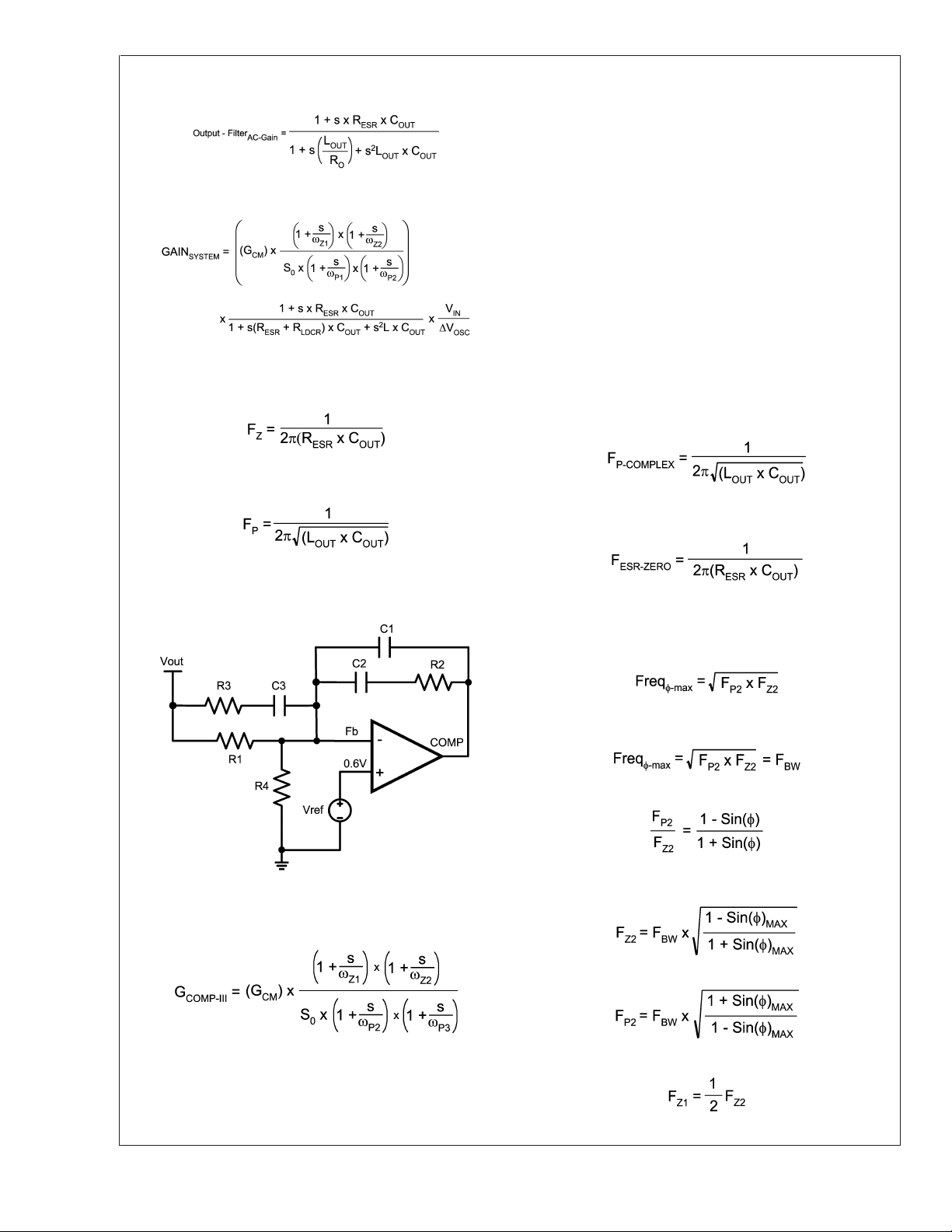
Application Information (Continued)
LM27241
Zero Frequency due to R
Complex Poles due to output inductor and output capacitors:
ESR
:
larger than the crossover frequency when ceramic capacitors are used. Rule of thumb is if F
ZERO
>
FBWuse type III
compensation.
and ωZ2: +20dB/DEC and +45DEG/DEC phase.
ω
Z1
: Adds phase lead in the vicinity of the crossover fre-
ω
Z2
quency.
and ωP2: -20dB/DEC and -45DEG/DEC phase.
ω
PZ1
Must be present to in the compensation to ensure the gain
rolls off at high frequency and prevent switching ripple from
disrupting the regulation of the converter.
The Loop Bandwidth ( F
frequency (F
) is usually set by the designer, with the
CROSS
) or known as the crossover
BW
basic guideline:
/10 ≤ FBW≤ FSW/5
F
SW
COMPENSATION DESIGN STEPS
Output Filter:
1) Choose crossover frequency
2) Determine complex pole frequency due to output filter:
Type III Compensator (PID)
FIGURE 16. Type III Compensator (PID)
20120148
3) Determine zero frequency due to R
ESR
Type III Compensator:
1) Frequency at which maximum phase boost occurs is at
the average between the frequency of F
P2
and F
Z2
Place this at the Crossover frequency:
where 60˚ ≥Φ
MAX
≥ 45˚
Type III Compensator Transfer Function
The Type III compensation is needed in designs where
output ceramic capacitors are used, and therefore is very
small. The Zero frequency, due to R
www.national.com 20
, is usually much
ESR

Application Information (Continued)
<
F
FZ2and F
Z1
DESIGN EXAMPLE
= 15V
V
IN
= 1.5V
V
OUT
= 300kHz
F
BW
BW = = 30kHz
L
= 2.2µH
OUT
= 2x100µF Tantalum + 2x47µF Ceramic
L
OUT
Tantalum = 100mΩ
R
ESR
Ceramic = 15mΩ
R
ESR
total = 294µF
C
OUT
R
total = 13mΩ
ESR
<
F
Z1
P-COMPLEX
C1= 190p F (use 220pF).
C
sets FBW:
3
R3=1kΩ
LM27241
Notice that F-zero due to the R
cross-over frequency (F
). TYPE III Compensation is re-
SW
is greater than the
ESR
quired.
Φ
45˚
MAX
Pick C2to be 4700pF, and calculate R2.C2= 4700 pF, & R2=
5.6 kΩ
R1=5kΩ
Set output voltage:
R4= 3.32kΩ
EVALUATION BOARD DETAILS
The Bill of Materials (BOM) is now provided for the LM27241
evaluation board. The schematic is the typical application
circuit. See Layout Guidelines for more guidance on preferred layout practices and also refer to Application Note
AN-1229. Note that a dual FET pack has been chosen for
the evaluation board.
The evaluation board has its output set to 1.5V. The rated
load 6A continuous, and 7A peak. A minimum load of 0.1mA
should be maintained on each output in SKIP mode, to
ensure regulation.
www.national.com21

LM27241
20120167
Typical Application (Expanded View)
FIGURE 17.
www.national.com 22

Bill of Materials
Designator Function Description Vendor
U1 Synchronous Buck Controller PWM Controller NSC
R1 Feedback Resistor 4.99 kΩ 1% 0805 VISHAY
R2 Compensation Resistor 5.62 kΩ 1% 0805 VISHAY
R3 Compensation Resistor 1.00 kΩ 1% 0805 VISHAY
R4 Feedback Resistor 3.32 kΩ 1% 0805 VISHAY
R5 Dynamic Feedback Resistor 40.2 kΩ 1% 0805 (Optional) VISHAY
R6 Enable pull up resistor 12.7 kΩ 1% 0805 VISHAY
R7 FPWM pull up resistor 12.7 kΩ 1% 0805 VISHAY
R8 Q3 Gate to GND resistor 10 kΩ 1% 0805 (Optional) VISHAY
R9 Freq Set Resistor 22.1 kΩ 1% 0805 VISHAY
R10 PGOOD pull up resistor 12.7 kΩ 1% 0805 VISHAY
R11 VDD filter resistor 10Ω 1% 0805 VISHAY
R12 Ilimit Resistor 1.33 kΩ 1% 0805 VISHAY
R13 Resistor (Optional) 0Ω VISHAY
R14 Snubber Resistor (Optional) 10Ω 5% 0805 VISHAY
C1 Compensation Capacitor 220 pF 0805 TDK
C2 Compensation Capacitor 4700 pF 0805 TDK
C3 Compensation Capacitor 2200 pF 0805 TDK
C4, C6, C8, C17 Ceramic Output Capacitor 47 µF 2220 6.3V TDK
C5, C8 Tantalum Output Capacitor 100 µF 4V B45192 EPCOS
C10 - C13 Ceramic/Tantalum Input Capacitors TDK/EPCOS
C14 Soft Start Capacitor 0.1 µF 0805 TDK
C15, C16 VDD Filter Capacitor 0.22 µF 0805 TDK
C19 VBOOST Capacitor 0.1 µF 0805 TDK
C20 Ceramic Input Capacitor 10 µF TDK
C21 Snubber Capacitor (Optional) 470 pF TDK
D2 VBOOST Diode BAT54 SOT23 Diodes INC
L1 Output Inductor HC1216 Falco Electronics
Q1 Top MOSFET IRF7821 International
Rectifier
Q2 Synchronous MOSFET IRF7832 International
Rectifier
Q3 Small Signal FET VDYNAMIC BSS138 SOT23 ON Semi
SW1 V-enable & FPWM/SKIP Set
SW2 Vdynamic Set
LM27241
www.national.com23

PCB Layout Diagrams
LM27241
20120162
FIGURE 18. Top Overlay
20120163
FIGURE 19. Top Layer
www.national.com 24
PCB Layout Diagrams (Continued)
LM27241
FIGURE 20. Internal Plane 1 (GND)
20120164
FIGURE 21. Internal Plane 2
20120165
www.national.com25

PCB Layout Diagrams (Continued)
LM27241
20120166
FIGURE 22. Bottom Layer
www.national.com 26
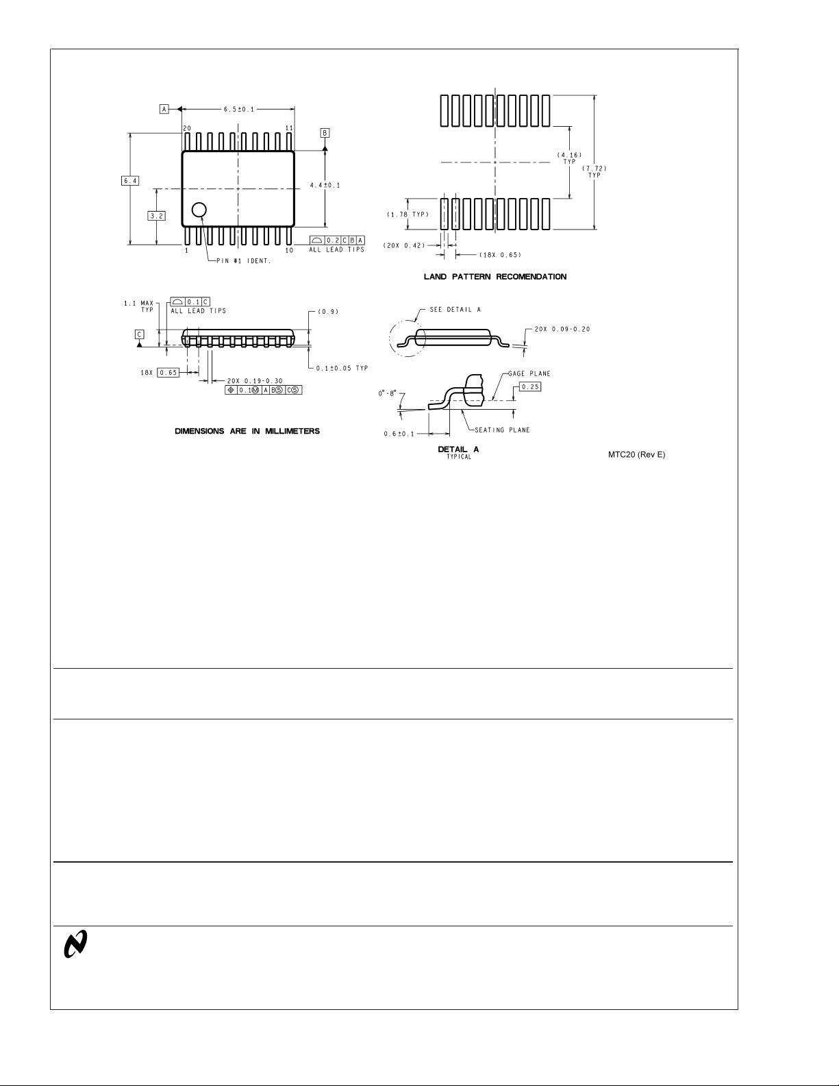
Physical Dimensions inches (millimeters) unless otherwise noted
LM27241 Synchronous Buck Regulator Controller for Mobile Systems
20-Lead TSSOP Package
NS Package Number MTC20
National does not assume any responsibility for use of any circuitry described, no circuit patent licenses are implied and National reserves
the right at any time without notice to change said circuitry and specifications.
For the most current product information visit us at www.national.com.
LIFE SUPPORT POLICY
NATIONAL’S PRODUCTS ARE NOT AUTHORIZED FOR USE AS CRITICAL COMPONENTS IN LIFE SUPPORT DEVICES OR SYSTEMS
WITHOUT THE EXPRESS WRITTEN APPROVAL OF THE PRESIDENT AND GENERAL COUNSEL OF NATIONAL SEMICONDUCTOR
CORPORATION. As used herein:
1. Life support devices or systems are devices or systems
which, (a) are intended for surgical implant into the body, or
(b) support or sustain life, and whose failure to perform when
properly used in accordance with instructions for use
2. A critical component is any component of a life support
device or system whose failure to perform can be reasonably
expected to cause the failure of the life support device or
system, or to affect its safety or effectiveness.
provided in the labeling, can be reasonably expected to result
in a significant injury to the user.
BANNED SUBSTANCE COMPLIANCE
National Semiconductor manufactures products and uses packing materials that meet the provisions of the Customer Products
Stewardship Specification (CSP-9-111C2) and the Banned Substances and Materials of Interest Specification (CSP-9-111S2) and contain
no ‘‘Banned Substances’’ as defined in CSP-9-111S2.
National Semiconductor
Americas Customer
Support Center
Email: new.feedback@nsc.com
Tel: 1-800-272-9959
www.national.com
National Semiconductor
Europe Customer Support Center
Fax: +49 (0) 180-530 85 86
Email: europe.support@nsc.com
Deutsch Tel: +49 (0) 69 9508 6208
English Tel: +44 (0) 870 24 0 2171
Français Tel: +33 (0) 1 41 91 8790
National Semiconductor
Asia Pacific Customer
Support Center
Email: ap.support@nsc.com
National Semiconductor
Japan Customer Support Center
Fax: 81-3-5639-7507
Email: jpn.feedback@nsc.com
Tel: 81-3-5639-7560
 Loading...