

February 2004
LM2716
Dual (Step-up and Step-down) PWM DC/DC Converter
LM2716 Dual (Step-up and Step-down) PWM DC/DC Converter
General Description
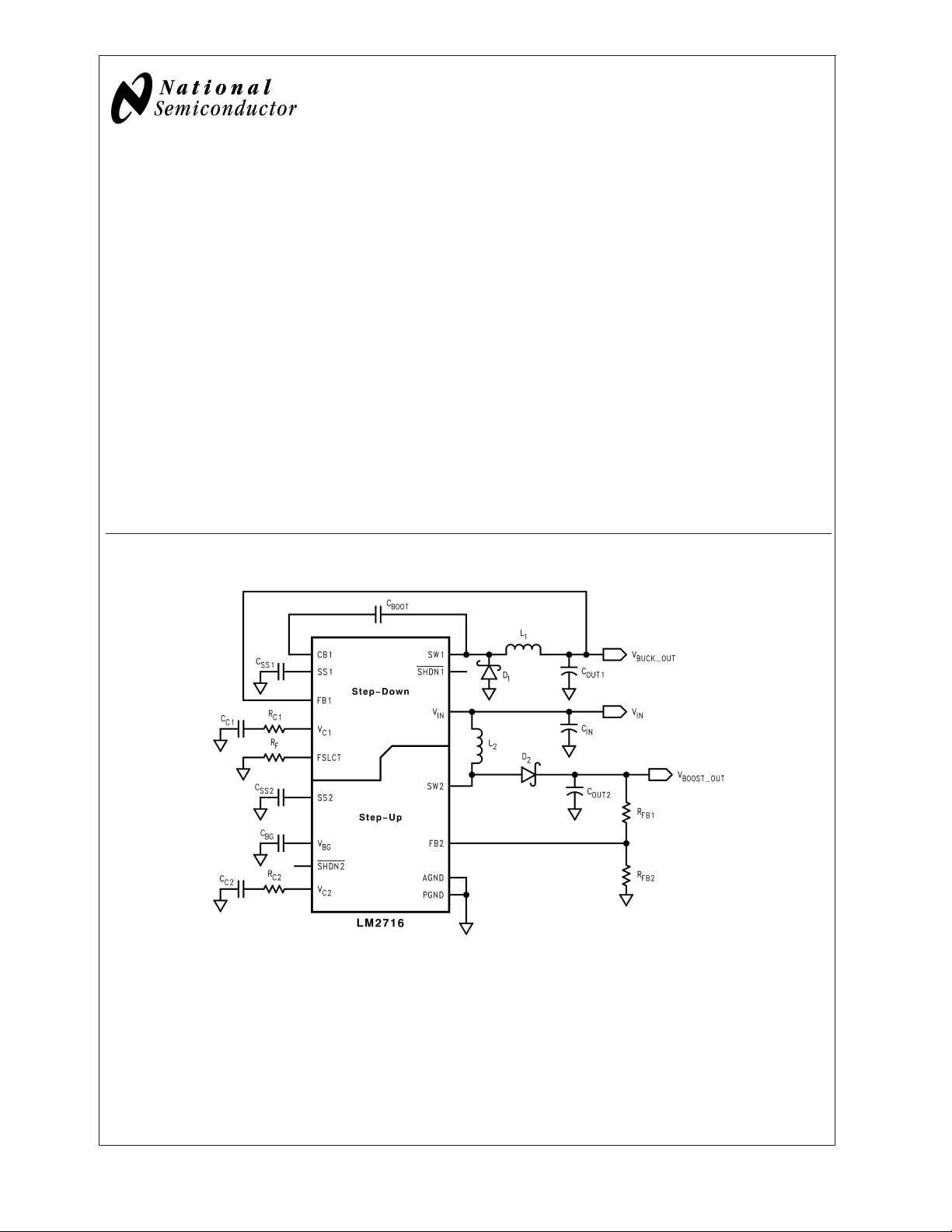
The LM2716 is composed of two PWM DC/DC converters. A
buck (step-down) converter is used to generate a fixed output voltage. A boost (step-up) converter is used to generate
an adjustable output voltage. Both converters feature low
(0.16Ω and 0.12Ω) internal switches for maximum
R
DSON
efficiency. Operating frequency can be adjusted anywhere
between 300kHz and 600kHz allowing the use of small
external components. External soft-start pins for each enables the user to tailor the soft-start times to a specific
application. Each converter may also be shut down independently with its own shutdown pin. The LM2716 is available in
a low profile 24-lead TSSOP package.
Typical Application Circuit
Features
n Fixed buck converter with a 1.8A, 0.16Ω, internal switch
n Adjustable boost converter with a 3.6A, 0.12Ω, internal
switch
n Adjustable boost output voltage up to 20V
n Operating input voltage range of 4V to 20V
n Input undervoltage protection
n 300kHz to 600kHz pin adjustable operating frequency
n Over temperature protection
n Small 24-Lead TSSOP package
n Patented current limit circuitry
Applications
n TFT-LCD Displays
n Handheld Devices
n Portable Applications
n Cellular Phones/Digital Camers
20071201
© 2004 National Semiconductor Corporation DS200712 www.national.com

Connection Diagram
LM2716
Top View
24-Lead TSSOP
20071204
Ordering Information
Order Number Package Type NSC Package Drawing Supplied As
LM2716MT-ADJ TSSOP-24 MTC24 61 Units, Rail
LM2716MTX-ADJ TSSOP-24 MTC24 2500 Units, Tape and Reel
www.national.com 2
Pin Description
Pin Name Function
1 PGND Power ground. AGND and PGND pins must be connected together directly at the part.
2 FB1 Buck output voltage feedback input.
3V
4V
C1
BG
5 SS2 Boost soft start pin.
6V
C2
7 FB2 Boost output voltage feedback input.
8 AGND Analog ground. AGND and PGND pins must be connected together directly at the part.
9 AGND Analog ground. AGND and PGND pins must be connected together directly at the part.
10 PGND Power ground. AGND and PGND pins must be connected together directly at the part.
11 PGND Power ground. AGND and PGND pins must be connected together directly at the part.
12 PGND Power ground. AGND and PGND pins must be connected together directly at the part.
13 SW2 Boost power switch input. Switch connected between SW2 pins and PGND pins. SW2
14 SW2 Boost power switch input. Switch connected between SW2 pins and PGND pins. SW2
15 SW2 Boost power switch input. Switch connected between SW2 pins and PGND pins. SW2
16 V
17 V
IN
IN
18 SHDN2
19 FSLCT Switching frequency select input. Use a resistor to set the frequency anywhere between
20 SS1 Buck soft start pin.
21 SHDN1
22 CB1 Buck converter bootstrap capacitor connection.
23 V
IN
24 SW1 Buck power switch input. Switch connected between V
Buck compensation network connection. Connected to the output of the voltage error
amplifier.
Bandgap connection.
Boost compensation network connection. Connected to the output of the voltage error
amplifier.
pins should be connected directly together at the device.
pins should be connected directly together at the device.
pins should be connected directly together at the device.
Analog power input. VINpins must be connected together directly at the DUT.
Analog power input. VINpins must be connected together directly at the DUT.
Shutdown pin for Boost converter. Active low.
300kHz and 600kHz.
Shutdown pin for Buck converter. Active low.
Analog power input. VINpins must be connected together directly at the DUT.
pins and SW1 pin.
IN
LM2716
www.national.com3
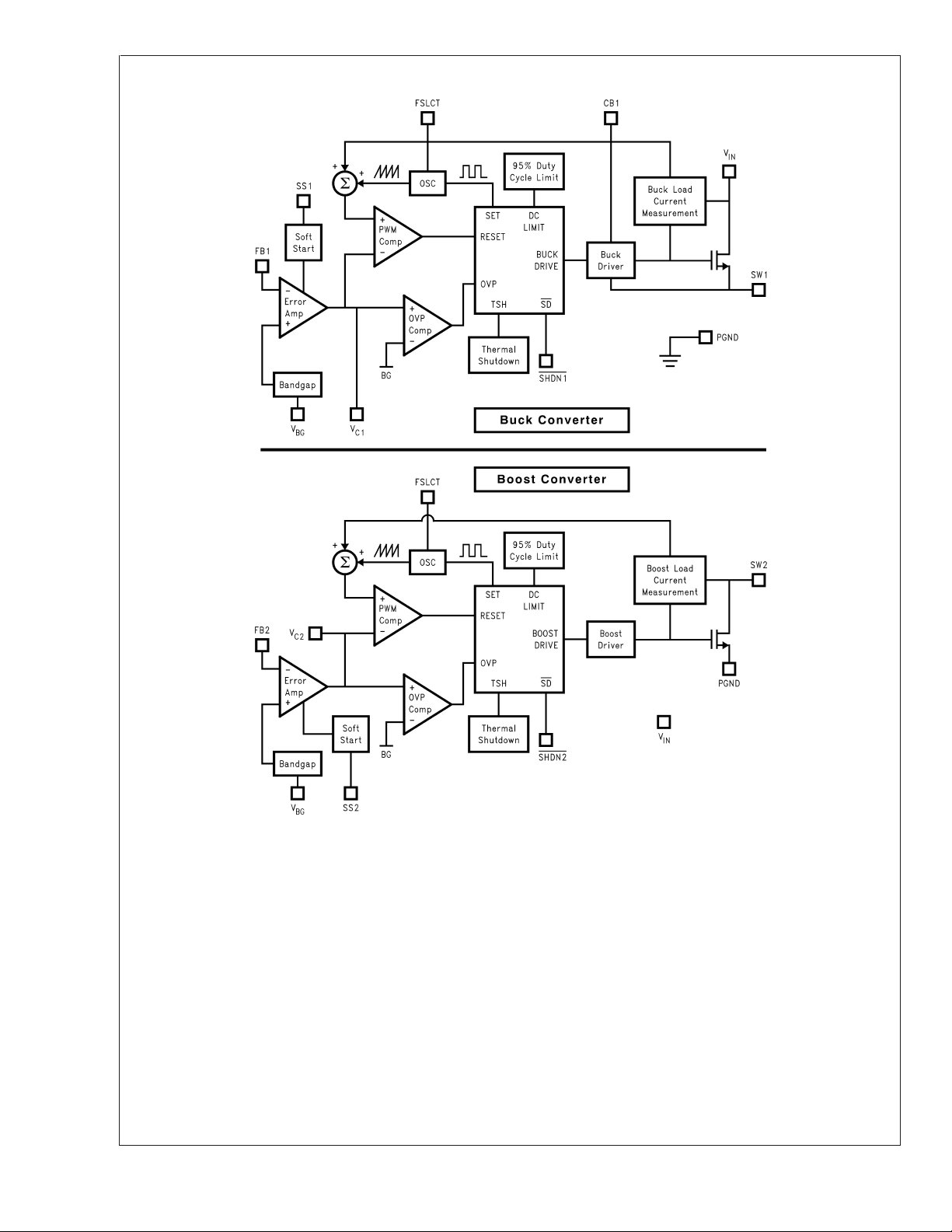
Block Diagram
LM2716
www.national.com 4
20071203

LM2716
Absolute Maximum Ratings (Note 1)
If Military/Aerospace specified devices are required,
please contact the National Semiconductor Sales Office/
Distributors for availability and specifications.
V
IN
SW1 Voltage −0.3V to 22V
SW2 Voltage −0.3V to 22V
−0.3V to 22V
Power Dissipation(Note 2) Internally Limited
Lead Temperature 300˚C
Vapor Phase (60 sec.) 215˚C
Infrared (15 sec.) 220˚C
ESD Susceptibility (Note 3)
Human Body Model 2kV
Machine Model 200V
FB1 Voltage −0.3V to 7V
FB2 Voltage −0.3V to 7V
V
Voltage 1.75V ≤ VC1≤ 2.25V
C1
V
Voltage 0.965V ≤ VC2≤ 1.565V
C2
SHDN1 Voltage
SHDN2 Voltage
−0.3V to 7.5V
−0.3V to 7.5V
SS1 Voltage −0.3V to 2.1V
SS2 Voltage −0.3V to 0.6V
FSLCT Voltage AGND to 5V
CB1 Voltage V
+7V(VIN=VSW)
IN
Operating Conditions
Operating Junction
Temperature Range
(Note 4) −40˚C to +125˚C
Storage Temperature −65˚C to +150˚C
Supply Voltage 4V to 20V
SW1 Voltage 20V
SW2 Voltage 20V
Maximum Junction Temperature 150˚C
Electrical Characteristics
Specifications in standard type face are for TJ= 25˚C and those with boldface type apply over the full Operating Temperature Range (T
Symbol Parameter Conditions
I
Q
V
BG
I
(Note 6) Buck Switch Current Limit 95% Duty Cycle (Note 7) 1.8 A
CL1
I
(Note 6) Boost Switch Current Limit 95% Duty Cycle (Note 7) 3.6 A
CL2
I
FB1
I
FB2
V
IN
g
m1
g
m2
A
V1
A
V2
D
MAX
F
SW
I
SHDN1
I
SHDN2
I
L1
I
L2
R
DSON1
R
DSON2
= −40˚C to +125˚C) Unless otherwise specified. VIN= 5V and IL= 0A, unless otherwise specified.
J
Total Quiescent Current (both
switchers)
Min
(Note 4)
Not Switching 2.8 3.5 mA
Switching, switch open 4 4.5 mA
V
=0V 9 15 µA
SHDN
Typ
(Note 5)
Max
(Note 4)
Bandgap Voltage 1.235 1.26 1.285 V
Buck FB Pin Bias Current
(Note 8)
Boost FB Pin Bias Current
(Note 8)
V
V
FB1
FB2
= 3.3V
= 1.265V
65 75 µA
27 55 nA
Input Voltage Range 420V
Buck Error Amp
Transconductance
Boost Error Amp
Transconductance
∆I = 20µA
∆I = 5µA
1200 µmho
175 µmho
Buck Error Amp Voltage Gain 100 V/V
Boost Error Amp Voltage
Gain
135 V/V
Maximum Duty Cycle 90 95 98 %
Switching Frequency RF= 47.5kΩ 250 300 350 kHz
R
= 22.6kΩ 500 600 700 kHz
F
Buck Shutdown Pin Current 0V<V
Boost Shutdown Pin Current 0V<V
SHDN1
SHDN2
<
7.5V −5 5 µA
<
7.5V −5 5 µA
Buck Switch Leakage Current VDS= 20V 0.2 5 µA
Boost Switch Leakage
Current
Buck Switch R
Boost Switch R
DSON
DSON
VDS= 20V
0.2 3 µA
160 mΩ
120 mΩ
Units
www.national.com5
Electrical Characteristics (Continued)
Specifications in standard type face are for TJ= 25˚C and those with boldface type apply over the full Operating Tempera-
LM2716
ture Range (T
Symbol Parameter Conditions
Th
SHDN1
Th
SHDN2
I
SS1
I
SS2
UVP On Threshold 3.35 3.8 4.0
θ
JA
Note 1: Absolute maximum ratings are limits beyond which damage to the device may occur. Operating Ratings are conditions for which the device is intended to
be functional, but device parameter specifications may not be guaranteed. For guaranteed specifications and test conditions, see the Electrical Characteristics.
Note 2: The maximum allowable power dissipation is a function of the maximum junction temperature, T
and the ambient temperature, T
temperature is calculated using: P
regulator will go into thermal shutdown.
Note 3: The human body model is a 100 pF capacitor discharged through a 1.5kΩ resistor into each pin. The machine model is a 200pF capacitor discharged
directly into each pin.
Note 4: All limits guaranteed at room temperature (standard typeface) and at temperature extremes (bold typeface). All room temperature limits are 100% tested
or guaranteed through statistical analysis. All limits at temperature extremes are guaranteed via correlation using standard Statistical Quality Control (SQC) methods.
All limits are used to calculate Average Outgoing Quality Level (AOQL).
Note 5: Typical numbers are at 25˚C and represent the most likely norm.
Note 6: Duty cycle affects current limit due to ramp generator.
Note 7: Current limit at 95% duty cycle. See TYPICAL PERFORMANCE section for Switch Current Limit vs. V
Note 8: Bias current flows into FB pin.
Note 9: Refer to National’s packaging website for more detailed thermal information and mounting techniques for the TSSOP package.
= −40˚C to +125˚C) Unless otherwise specified. VIN= 5V and IL= 0A, unless otherwise specified.
J
Min
(Note 4)
Typ
(Note 5)
Max
(Note 4)
Buck SHDN Threshold Output High 1.37 2
Output Low 0.8 1.35
Boost SHDN Threshold Output High 1.37 2
Output Low 0.8 1.35
Buck Soft Start Pin Current 6 9.5 12 µA
Boost Soft Start Pin Current 15 19 22 µA
Off Threshold 3.10 3.6 3.9
Thermal Resistance
TSSOP, package only 115
(Note 9)
(MAX), the junction-to-ambient thermal resistance, θJA,
. See the Electrical Characteristics table for the thermal resistance. The maximum allowable power dissipation at any ambient
A
(MAX) = (T
D
J(MAX)−TA
)/θJA. Exceeding the maximum allowable power dissipation will cause excessive die temperature, and the
J
IN
Units
V
V
V
˚C/W
www.national.com 6

Typical Performance Characteristics
Switching Frequency vs. RFResistor
20071223
Switching Frequency vs. Input Voltage
= 600kHz)
(F
SW
LM2716
Switching Frequency vs. Input Voltage
(FSW= 300kHz)
20071224
Buck Efficiency vs. Load Current
(FSW= 300kHz)
20071225
Buck Efficiency vs. Load Current
= 600kHz)
(F
SW
20071226
Boost Efficiency vs. Load Current
(FSW= 300kHz)
20071227 20071231
www.national.com7

Typical Performance Characteristics (Continued)
LM2716
Boost Efficiency vs. Load Current
(F
= 600kHz) Boost Switch R
SW
20071232
vs. Input Voltage
DSON
20071235
www.national.com 8

Buck Operation
PROTECTION (BOTH REGULATORS)
The LM2716 has dedicated protection circuitry running during normal operation to protect the IC. The Thermal Shutdown circuitry turns off the power devices when the die
temperature reaches excessive levels. The UVP comparator
protects the power devices during supply power startup and
shutdown to prevent operation at voltages less than the
minimum input voltage. The OVP comparator is used to
prevent the output voltage from rising at no loads allowing
full PWM operation over all load conditions. The LM2716
also features a shutdown mode for each converter decreasing the supply current to 9µA (both in shutdown mode).
LM2716
changing) load conditions. For higher output current applications or dynamic load conditions a 68µF to 100µF low ESR
capacitor is recommended. It is also recommended to put a
small ceramic capacitor (0.1 µF) between the input pin and
ground pin to reduce high frequency spikes.
INDUCTOR SELECTION
The most critical parameters for the inductor are the inductance, peak current and the DC resistance. The inductance
is related to the peak-to-peak inductor ripple current, the
input and the output voltages:
CONTINUOUS CONDUCTION MODE
The LM2716 contains a current-mode, PWM buck regulator.
A buck regulator steps the input voltage down to a lower
output voltage. In continuous conduction mode (when the
inductor current never reaches zero at steady state), the
buck regulator operates in two cycles. The power switch is
connected between V
and SW1.
IN
In the first cycle of operation the transistor is closed and the
diode is reverse biased. Energy is collected in the inductor
and the load current is supplied by C
and the rising
OUT
current through the inductor.
During the second cycle the transistor is open and the diode
is forward biased due to the fact that the inductor current
cannot instantaneously change direction. The energy stored
in the inductor is transferred to the load and output capacitor.
The ratio of these two cycles determines the output voltage.
The output voltage is defined approximately as:
where D is the duty cycle of the switch, D and D' will be
required for design calculations.
DESIGN PROCEDURE
This section presents guidelines for selecting external components.
INPUT CAPACITOR
A low ESR aluminum, tantalum, or ceramic capacitor is
needed betwen the input pin and power ground. This capacitor prevents large voltage transients from appearing at the
input. The capacitor is selected based on the RMS current
and voltage requirements. The RMS current is given by:
The RMS current reaches its maximum (I
equals 2V
V
IN
. This value should be increased by 50% to
OUT
OUT
/2) when
account for the ripple current increase due to the boost
regulator. For an aluminum or ceramic capacitor, the voltage
rating should be at least 25% higher than the maximum input
voltage. If a tantalum capacitor is used, the voltage rating
required is about twice the maximum input voltage. The
tantalum capacitor should be surge current tested by the
manufacturer to prevent being shorted by the inrush current.
The minimum capacitor value should be 47µF for lower
output load current applications and less dynamic (quickly
A higher value of ripple current reduces inductance, but
increases the conductance loss, core loss, current stress for
the inductor and switch devices. It also requires a bigger
output capacitor for the same output voltage ripple requirement. A reasonable value is setting the ripple current to be
30% of the DC output current. Since the ripple current increases with the input voltage, the maximum input voltage is
always used to determine the inductance. The DC resistance
of the inductor is a key parameter for the efficiency. Lower
DC resistance is available with a bigger winding area. A good
tradeoff between the efficiency and the core size is letting the
inductor copper loss equal 2% of the output power.
OUTPUT CAPACITOR
The selection of C
is driven by the maximum allowable
OUT
output voltage ripple. The output ripple in the constant frequency, PWM mode is approximated by:
The ESR term usually plays the dominant role in determining
the voltage ripple. A low ESR aluminum electrolytic or tantalum capacitor (such as Nichicon PL series, Sanyo OS-CON,
Sprague 593D, 594D, AVX TPS, and CDE polymer aluminum) is recommended. An electrolytic capacitor is not recommended for temperatures below −25˚C since its ESR
rises dramatically at cold temperature. A tantalum capacitor
has a much better ESR specification at cold temperature and
is preferred for low temperature applications.
BOOT CAPACITOR
A 3.3 nF ceramic capacitor is recommended for the bootstrap capacitor.
SOFT-START CAPACITOR (BOTH REGULATORS)
The SS pins are used to tailor the soft-start for a specific
application. A current source charges the external soft-start
capacitor, C
. The soft-start time can be estimated as:
SS
T
SS=CSS
*0.6V/I
SS
Soft-start times may be implemented using the SS pin and a
capacitor C
.
SS
When programming the softstart time, simply use the equation given in the Soft-Start Capacitor section above. This
equation uses the typical room temperature value of the soft
start current to set the soft start time.
www.national.com9

Buck Operation (Continued)
COMPENSATION COMPONENTS
LM2716
In the control to output transfer function, the first pole F
can be estimated as 1/(2πR
OUTCOUT
the output capacitor is 1/(2πESRC
frequency pole F
whereD=V
IN
and V
and V
in the range of 45kHz to 150kHz:
P2
F
P2=FSW
, n = 1+0.348L/(VIN−V
OUT/VIN
in volts).
OUT
The total loop gain G is approximately 500/I
is in amperes.
A Gm amplifier is used inside the LM2716. The output resis-
of the Gm amplifier is about 85kΩ.CC1and R
tor R
o
together with Rogive a lag compensation to roll off the gain:
); The ESR zero FZ1of
); Also, there is a high
OUT
/(πn(1−D))
OUT
OUT
P1
)(LisinµHs
where I
OUT
C1
F
= 1/(2πCC1(Ro+RC1)), F
PC1
In some applications, the ESR zero F
. Then, CC3is needed to introduce F
by F
P2
ESR zero, F
= 1/(2πCC3Ro\RC1).
P2
= 1/2πCC1RC1.
ZC1
can not be cancelled
Z1
to cancel the
PC2
The rule of thumb is to have more than 45˚ phase margin at
the crossover frequency (G=1).
SCHOTTKY DIODE
The breakdown voltage rating of D
is preferred to be 25%
1
higher than the maximum input voltage. Since D1 is only on
for a short period of time, the average current rating for D1
only requires being higher than 30% of the maximum output
current.
www.national.com 10

Boost Operation
LM2716
20071202
FIGURE 1. Simplified Boost Converter Diagram
(a) First Cycle of Operation (b) Second Cycle Of Operation
CONTINUOUS CONDUCTION MODE
The LM2716 contains a current-mode, PWM boost regulator.
A boost regulator steps the input voltage up to a higher
output voltage. In continuous conduction mode (when the
inductor current never reaches zero at steady state), the
boost regulator operates in two cycles.
In the first cycle of operation, shown in Figure 1 (a), the
transistor is closed and the diode is reverse biased. Energy
is collected in the inductor and the load current is supplied by
.
C
OUT
The second cycle is shown in Figure 1 (b). During this cycle,
the transistor is open and the diode is forward biased. The
energy stored in the inductor is transferred to the load and
output capacitor.
The ratio of these two cycles determines the output voltage.
The output voltage is defined approximately as:
where D is the duty cycle of the switch, D and D' will be
required for design calculations.
INTRODUCTION TO COMPENSATION
SETTING THE OUTPUT VOLTAGE
The output voltage is set using the feedback pin and a
resistor divider connected to the output as shown in Figure 3.
The feedback pin voltage is 1.26V, so the ratio of the feedback resistors sets the output voltage according to the following equation:
20071205
FIGURE 2. (a) Inductor current. (b) Diode current.
www.national.com11

Boost Operation (Continued)
The LM2716 has a current mode PWM boost converter. The
LM2716
signal flow of this control scheme has two feedback loops,
one that senses switch current and one that senses output
voltage.
To keep a current programmed control converter stable
above duty cycles of 50%, the inductor must meet certain
criteria. The inductor, along with input and output voltage,
will determine the slope of the current through the inductor
(see Figure 2 (a)). If the slope of the inductor current is too
great, the circuit will be unstable above duty cycles of 50%.
If the duty cycle is approaching the maximum of 85%, it may
be necessary to increase the inductance by as much as 2X.
See Inductor and Diode Selection for more detailed inductor
sizing.
The LM2716 provides a compensation pin (V
ize the voltage loop feedback. It is recommended that a
series combination of R
and CC2be used for the compen-
C2
sation network, as shown in Figure 3. For any given application, there exists a unique combination of R
that will optimize the performance of the LM2716 circuit in
terms of its transient response. The series combination of
and CC2introduces a pole-zero pair according to the
R
C2
following equations:
where ROis the output impedance of the error amplifier,
approximately 850kΩ. For most applications, performance
can be optimized by choosing values within the range 5kΩ≤
≤ 20kΩ (RC2can be up to 200kΩ if CC4is used, see
R
C2
High Output Capacitor ESR Compensation) and 680pF ≤
≤ 4.7nF. Refer to the Applications Information section for
C
C2
recommended values for specific circuits and conditions.
Refer to the Compensation section for other design requirement.
COMPENSATION
This section will present a general design procedure to help
insure a stable and operational circuit. The designs in this
datasheet are optimized for particular requirements. If different conversions are required, some of the components may
need to be changed to ensure stability. Below is a set of
general guidelines in designing a stable circuit for continuous conduction operation (loads greater than approximately
100mA), in most all cases this will provide for stability during
discontinuous operation as well. The power components and
their effects will be determined first, then the compensation
components will be chosen to produce stability.
INDUCTOR AND DIODE SELECTION
Although the inductor sizes mentioned earlier are fine for
most applications, a more exact value can be calculated. To
ensure stability at duty cycles above 50%, the inductor must
have some minimum value determined by the minimum
input voltage and the maximum output voltage. This equation is:
C2
) to custom-
and C
C2
C2
where FSWis the switching frequency, D is the duty cycle,
and R
from the graph "Boost Switch R
is the ON resistance of the internal switch taken
DSON
vs. Input Voltage" in the
DSON
Typical Performance Characteristics section. This equation
>
is only good for duty cycles greater than 50% (D
0.5), for
duty cycles less than 50% the recommended values may be
used. The corresponding inductor current ripple as shown in
Figure 2 (a) is given by:
The inductor ripple current is important for a few reasons.
One reason is because the peak switch current will be the
average inductor current (input current or I
/D’) plus ∆iL.
LOAD
As a side note, discontinuous operation occurs when the
inductor current falls to zero during a switching cycle, or ∆i
is greater than the average inductor current. Therefore, continuous conduction mode occurs when ∆i
is less than the
L
average inductor current. Care must be taken to make sure
that the switch will not reach its current limit during normal
operation. The inductor must also be sized accordingly. It
should have a saturation current rating higher than the peak
inductor current expected. The output voltage ripple is also
affected by the total ripple current.
The output diode for a boost regulator must be chosen
correctly depending on the output voltage and the output
current. The typical current waveform for the diode in continuous conduction mode is shown in Figure 2 (b). The diode
must be rated for a reverse voltage equal to or greater than
the output voltage used. The average current rating must be
greater than the maximum load current expected, and the
peak current rating must be greater than the peak inductor
current. During short circuit testing, or if short circuit conditions are possible in the application, the diode current rating
must exceed the switch current limit. Using Schottky diodes
with lower forward voltage drop will decrease power dissipation and increase efficiency.
DC GAIN AND OPEN-LOOP GAIN
Since the control stage of the converter forms a complete
feedback loop with the power components, it forms a closedloop system that must be stabilized to avoid positive feedback and instability. A value for open-loop DC gain will be
required, from which you can calculate, or place, poles and
zeros to determine the crossover frequency and the phase
margin. A high phase margin (greater than 45˚) is desired for
the best stability and transient response. For the purpose of
stabilizing the LM2716, choosing a crossover point well below where the right half plane zero is located will ensure
sufficient phase margin. A discussion of the right half plane
zero and checking the crossover using the DC gain will
follow.
OUTPUT CAPACITOR SELECTION
The choice of output capacitors is somewhat arbitrary and
depends on the design requirements for output voltage
ripple. It is recommended that low ESR (Equivalent Series
L
www.national.com 12

Boost Operation (Continued)
Resistance, denoted R
ceramic, polymer electrolytic, or low ESR tantalum. Higher
ESR capacitors may be used but will require more compensation which will be explained later on in the section. The
ESR is also important because it determines the peak to
peak output voltage ripple according to the approximate
equation:
∆V
OUT
A minimum value of 10µF is recommended and may be
increased to a larger value. After choosing the output capacitor you can determine a pole-zero pair introduced into the
control loop by the following equations:
Where RLis the minimum load resistance corresponding to
the maximum load current. The zero created by the ESR of
the output capacitor is generally very high frequency if the
ESR is small. If low ESR capacitors are used it can be
neglected. If higher ESR capacitors are used see the High
Output Capacitor ESR Compensation section.
RIGHT HALF PLANE ZERO
A current mode control boost regulator has an inherent right
half plane zero (RHP zero). This zero has the effect of a zero
in the gain plot, causing an imposed +20dB/decade on the
rolloff, but has the effect of a pole in the phase, subtracting
another 90˚ in the phase plot. This can cause undesirable
effects if the control loop is influenced by this zero. To ensure
the RHP zero does not cause instability issues, the control
loop should be designed to have a bandwidth of less than
the frequency of the RHP zero. This zero occurs at a frequency of:
) capacitors be used such as
ESR
) 2∆iLR
ESR
(in Volts)
1
LM2716
pected loads and then set the zero f
mately in the middle. The frequency of this zero is determined by:
Now RC2can be chosen with the selected value for CC2.
Check to make sure that the pole f
500Hz range, change each value slightly if needed to ensure
both component values are in the recommended range. After
checking the design at the end of this section, these values
can be changed a little more to optimize performance if
desired. This is best done in the lab on a bench, checking the
load step response with different values until the ringing and
overshoot on the output voltage at the edge of the load steps
is minimal. This should produce a stable, high performance
circuit. For improved transient response, higher values of
should be chosen. This will improve the overall band-
R
C2
width which makes the regulator respond more quickly to
transients. If more detail is required, or the most optimal
performance is desired, refer to a more in depth discussion
of compensating current mode DC/DC switching regulators.
HIGH OUTPUT CAPACITOR ESR COMPENSATION
When using an output capacitor with a high ESR value, or
just to improve the overall phase margin of the control loop,
another pole may be introduced to cancel the zero created
by the ESR. This is accomplished by adding another capaci-
, directly from the compensation pin VC2to ground, in
tor, C
C4
parallel with the series combination of R
pole should be placed at the same frequency as f
zero. The equation for this pole follows:
⁄
2
To ensure this equation is valid, and that CC4can be used
without negatively impacting the effects of R
must be greater than 10fZC.
to a point approxi-
ZC
is still in the 10Hz to
PC
and CC2. The
C2
Z1
and CC2,f
C2
, the ESR
PC4
where I
is the maximum load current.
LOAD
SELECTING THE COMPENSATION COMPONENTS
The first step in selecting the compensation components
R
and CC2is to set a dominant low frequency pole in the
C2
control loop. Simply choose values for R
and CC2within
C2
the ranges given in the Introduction to Compensation section
to set this pole in the area of 10Hz to 500Hz. The frequency
of the pole created is determined by the equation:
where ROis the output impedance of the error amplifier,
approximately 850kΩ. Since R
, it does not have much effect on the above equation and
R
O
can be neglected until a value is chosen to set the zero f
is created to cancel out the pole created by the output
f
ZC
capacitor, f
. The output capacitor pole will shift with differ-
P1
is generally much less than
C2
ZC
ent load currents as shown by the equation, so setting the
zero is not exact. Determine the range of f
over the ex-
P1
CHECKING THE DESIGN
The final step is to check the design. This is to ensure a
bandwidth of
This is done by calculating the open-loop DC gain, A
1
⁄2or less of the frequency of the RHP zero.
. After
DC
this value is known, you can calculate the crossover visually
by placing a −20dB/decade slope at each pole, and a +20dB/
decade slope for each zero. The point at which the gain plot
crosses unity gain, or 0dB, is the crossover frequency. If the
crossover frequency is less than
1
⁄2the RHP zero, the phase
margin should be high enough for stability. The phase margin can also be improved by adding C
in the section. The equation for A
as discussed earlier
C4
is given below with
DC
additional equations required for the calculation:
.
www.national.com13

Boost Operation (Continued)
LM2716
mc ) 0.072FSW(in V/s)
where RLis the minimum load resistance, VINis the maximum input voltage, g
tance found in the Electrical Characteristics table, and R
is the value chosen from the graph "R
SON
the Typical Performance Characteristics section.
LAYOUT CONSIDERATIONS
The LM2716 uses two separate ground connections, PGND
for the drivers and boost NMOS power device and AGND for
the sensitive analog control circuitry. The AGND and PGND
pins should be tied directly together at the package. The
feedback and compensation networks should be connected
is the error amplifier transconduc-
m
DSON2
Application Information
Some recommended Inductors (others may be used)
Manufacturer Inductor Contact Information
Coilcraft DO3316 and DO5022 series www.coilcraft.com
Coiltronics DRQ73 and CD1 series www.cooperet.com
Pulse P0751 and P0762 series www.pulseeng.com
Sumida CDRH8D28 and CDRH8D43 series www.sumida.com
vs. VIN"in
D
directly to a dedicated analog ground plane and this ground
plane must connect to the AGND pin. If no analog ground
plane is available then the ground connections of the feedback and compensation networks must tie directly to the
AGND pin. Connecting these networks to the PGND can
inject noise into the system and effect performance.
The input bypass capacitor C
, as shown in Figure 3, must
IN
be placed close to the IC. This will reduce copper trace
resistance which effects input voltage ripple of the IC. For
additional input voltage filtering, a 100nF bypass capacitor
can be placed in parallel with C
, close to the VINpin, to
IN
shunt any high frequency noise to ground. The output capacitors, C
OUT1
and C
the IC. Any copper trace connections for the C
, should also be placed close to
OUT2
OUTX
capacitors can increase the series resistance, which directly effects
output voltage ripple. The feedback network, resistors R
-
and R
the inductor, to minimize copper trace connections that can
, should be kept close to the FB pin, and away from
FB2
FB1
inject noise into the system. Trace connections made to the
inductors and schottky diodes should be minimized to reduce power dissipation and increase overall efficiency. See
Figure 3, Figure 4, and Figure 5 for a good example of
proper layout. For more detail on switching power supply
layout considerations see Application Note AN-1149: Layout
Guidelines for Switching Power Supplies.
Some recommended Input and Output Capacitors (others may be used)
Manufacturer Capacitor Contact Information
Vishay Sprague 293D, 592D, and 595D series tantalum www.vishay.com
Taiyo Yuden High capacitance MLCC ceramic www.t-yuden.com
Cornell Dubilier
Panasonic
ESRD seriec Polymer Aluminum Electrolytic
SPV and AFK series V-chip series
High capacitance MLCC ceramic
EEJ-L series tantalum
www.cde.com
www.panasonic.com
www.national.com 14

Application Information (Continued)
LM2716
FIGURE 3. 15V, 3.3V Output Application
20071257
FIGURE 4. PCB Layout, Top
20071258
www.national.com15

Application Information (Continued)
LM2716
FIGURE 5. PCB Layout, Bottom
20071259
www.national.com 16

Physical Dimensions inches (millimeters)
unless otherwise noted
LM2716 Dual (Step-up and Step-down) PWM DC/DC Converter
TSSOP-24 Pin Package (MTC)
For Ordering, Refer to Ordering Information Table
NS Package Number MTC24
LIFE SUPPORT POLICY
NATIONAL’S PRODUCTS ARE NOT AUTHORIZED FOR USE AS CRITICAL COMPONENTS IN LIFE SUPPORT
DEVICES OR SYSTEMS WITHOUT THE EXPRESS WRITTEN APPROVAL OF THE PRESIDENT AND GENERAL
COUNSEL OF NATIONAL SEMICONDUCTOR CORPORATION. As used herein:
1. Life support devices or systems are devices or
systems which, (a) are intended for surgical implant
into the body, or (b) support or sustain life, and
whose failure to perform when properly used in
accordance with instructions for use provided in the
2. A critical component is any component of a life
support device or system whose failure to perform
can be reasonably expected to cause the failure of
the life support device or system, or to affect its
safety or effectiveness.
labeling, can be reasonably expected to result in a
significant injury to the user.
BANNED SUBSTANCE COMPLIANCE
National Semiconductor certifies that the products and packing materials meet the provisions of the Customer Products
Stewardship Specification (CSP-9-111C2) and the Banned Substances and Materials of Interest Specification
(CSP-9-111S2) and contain no ‘‘Banned Substances’’ as defined in CSP-9-111S2.
National Semiconductor
Americas Customer
Support Center
Email: new.feedback@nsc.com
Tel: 1-800-272-9959
www.national.com
National does not assume any responsibility for use of any circuitry described, no circuit patent licenses are implied and National reserves the right at any time without notice to change said circuitry and specifications.
National Semiconductor
Europe Customer Support Center
Fax: +49 (0) 180-530 85 86
Email: europe.support@nsc.com
Deutsch Tel: +49 (0) 69 9508 6208
English Tel: +44 (0) 870 24 0 2171
Français Tel: +33 (0) 1 41 91 8790
National Semiconductor
Asia Pacific Customer
Support Center
Email: ap.support@nsc.com
National Semiconductor
Japan Customer Support Center
Fax: 81-3-5639-7507
Email: jpn.feedback@nsc.com
Tel: 81-3-5639-7560
 Loading...