

LM22674
500 mA SIMPLE SWITCHER®, Step-Down Voltage
Regulator with Precision Enable
LM22674 500 mA SIMPLE SWITCHER®, Step-Down Voltage Regulator with Precision Enable
October 17, 2008
General Description
The LM22674 series of regulators are monolithic integrated
circuits which provide all of the active functions for a stepdown (buck) switching regulator capable of driving up to 500
mA loads with excellent line and load regulation characteristics. High efficiency (>90%) is obtained through the use of a
low ON-resistance N-channel MOSFET. The series consists
of a fixed 5V output and an adjustable version.
The SIMPLE SWITCHER® concept provides for an easy to
use complete design using a minimum number of external
components and National’s WEBENCH® design tool.
National’s WEBENCH® tool includes features such as external component calculation, electrical simulation, thermal simulation, and Build-It boards for easy design-in. The switching
clock frequency is provided by an internal fixed frequency oscillator which operates at 500 kHz. The LM22674 series also
has built in thermal shutdown, current limiting and an enable
control input that can power down the regulator to a low 25
µA quiescent current standby condition.
Features
Wide input voltage range: 4.5V to 42V
■
Internally compensated voltage mode control
■
Stable with low ESR ceramic capacitors
■
200 mΩ N-channel MOSFET
■
Output voltage options:
■
-ADJ (outputs as low as 1.285V)
-5.0 (output fixed to 5V)
±1.5% feedback reference accuracy
■
Switching frequency of 500 kHz
■
-40°C to 125°C operating junction temperature range
■
Precision enable pin
■
Integrated boot diode
■
Integrated soft-start
■
Fully WEBENCH® enabled
■
Step-down and inverting buck-boost applications
■
Package
PSOP-8 (Exposed Pad)
■
Applications
Industrial Control
■
Telecom and Datacom Systems
■
Embedded Systems
■
Automotive Telematics and Body Electronics
■
Conversions from Standard 24V, 12V and 5V Input Rails
■
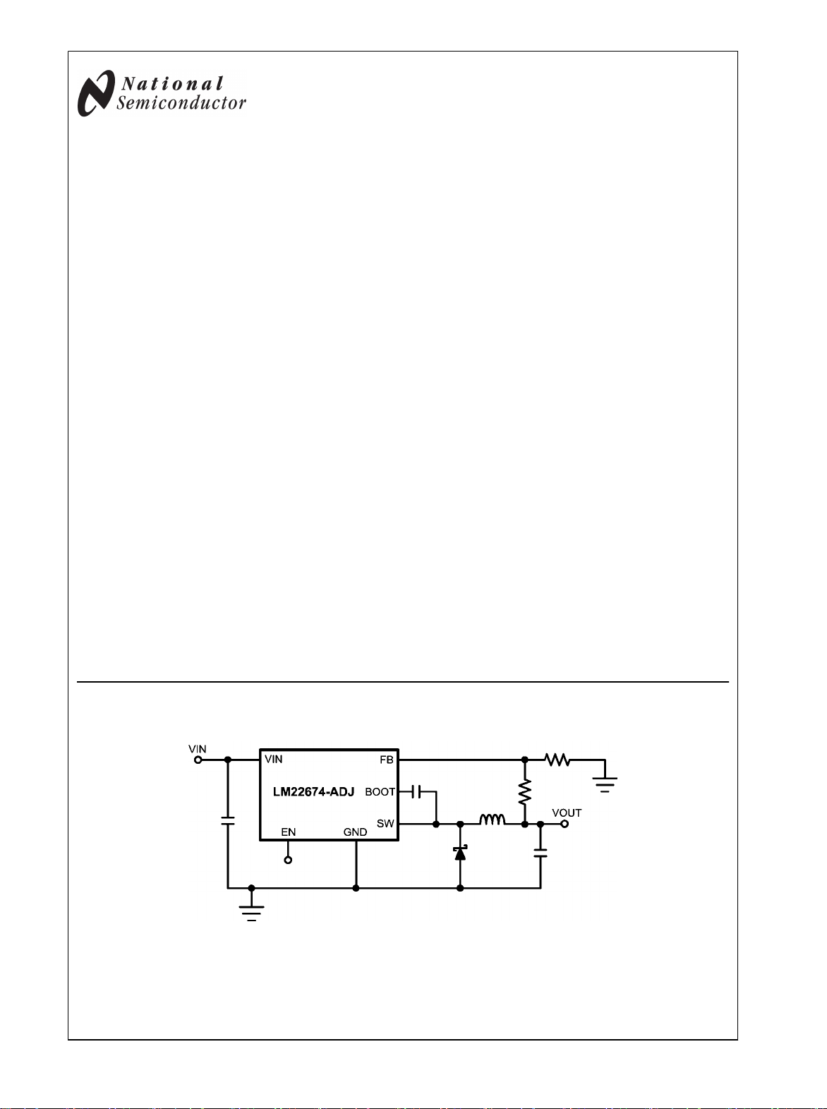
Simplified Application Schematic
30076901
© 2008 National Semiconductor Corporation 300769 www.national.com
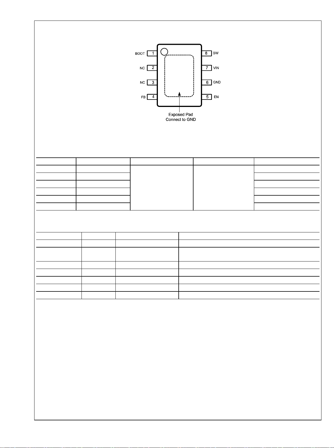
Connection Diagram
LM22674
8-Lead Plastic PSOP-8 Package
NS Package Number MRA08B
30076940
Ordering Information
Output Voltage Order Number Package Type NSC Package Drawing Supplied As
ADJ LM22674MR-ADJ
ADJ LM22674MRE-ADJ 250 Units in Tape and Reel
ADJ LM22674MRX-ADJ 2500 Units in Tape and Reel
5.0 LM22674MR-5.0 95 Units in Rails
5.0 LM22674MRE-5.0 250 Units in Tape and Reel
5.0 LM22674MRX-5.0 2500 Units in Tape and Reel
PSOP-8 Exposed Pad MRA08B
95 Units in Rails
Pin Descriptions
Pins Name Description Application Information
1 BOOT Bootstrap input Provides the gate voltage for the high side NFET.
2, 3 NC Not Connected Pins are not electrically connected inside the chip. Pins do function
as thermal conductor.
4 FB Feedback pin Inverting input to the internal voltage error amplifier.
5 EN Precision enable pin When pulled low regulator turns off.
6 GND System ground Provide good capacitive decoupling between VIN and this pin
7 VIN Source input voltage Input to the regulator. Operates from 4.5V to 42V.
8 SW Switch pin Attaches to the switch node
www.national.com 2
LM22674
Absolute Maximum Ratings (Note 1)
If Military/Aerospace specified devices are required,
please contact the National Semiconductor Sales Office/
Distributors for availability and specifications.
VIN to GND 43V
EN Pin Voltage -0.5V to 6V
SW to GND (Note 2) -5V to V
IN
BOOT Pin Voltage VSW + 7V
FB Pin Voltage -0.5V to 7V
Power Dissipation Internally Limited
Junction Temperature 150°C
Electrical Characteristics Limits in standard type are for T
Soldering Information
Vapor Phase (75 sec.) 219°C
Infrared (10 sec.) 240°C
Wave (4 sec.) 260°C
ESD Rating (Note 3)
Human Body Model ±2 kV
Storage Temperature Range -65°C to +150°C
Operating Ratings (Note 1)
Supply Voltage (VIN)
Junction Temperature Range -40°C to +125°C
= 25°C only; limits in boldface type apply over the
J
4.5V to 42V
junction temperature (TJ) range of -40°C to +125°C. Minimum and Maximum limits are guaranteed through test, design, or statistical
correlation. Typical values represent the most likely parametric norm at TA = TJ = 25°C, and are provided for reference purposes
only. Unless otherwise specified: VIN = 12V.
Symbol Parameter Conditions Min
(Note 5)
Typ
(Note 4)
Max
(Note 5)
LM22674-5.0
V
FB
Feedback Voltage VIN = 8V to 42V 4.925/4.9 5.0 5.075/5.1 V
LM22674-ADJ
V
FB
Feedback Voltage VIN = 4.7V to 42V 1.266/1.259 1.285 1.304/1.311 V
All Output Voltage Versions
I
I
STDBY
I
CL
I
Q
L
Quiescent Current VFB = 5V 3.4 6 mA
Standby Quiescent Current EN Pin = 0V 25 40 µA
Current Limit 0.56/0.62 0.7 0.84/0.9 A
Output Leakage Current VIN = 42V, EN Pin = 0V, VSW = 0V 0.2 2 µA
VSW = -1V 0.1 3 µA
R
DS(ON)
f
T
OFFMIN
T
ONMIN
I
BIAS
V
I
EN
T
O
EN
SD
Switch On-Resistance 0.2 0.24/0.32
Oscillator Frequency 400 500 600 kHz
Minimum Off-time 300 ns
Minimum On-time 100 ns
Feedback Bias Current VFB = 1.3V (ADJ Version Only) 230 nA
Enable Threshold Voltage 1.3 1.6 1.9 V
Enable Input Current EN Input = 0V 6 µA
Thermal Shutdown
150 °C
Threshold
θ
JA
Thermal Resistance MR package, Junction to ambient
60 °C/W
temperature resistance (Note 6)
Units
Ω
3 www.national.com
Note 1: Absolute Maximum Ratings indicate limits beyond which damage to the device may occur, including inoperability and degradation of device reliability
and/or performance. Functional operation of the device and/or non-degradation at the Absolute Maximum Ratings or other conditions beyond those indicated in
the recommended Operating Ratings is not implied. The recommended Operating Ratings indicate conditions at which the device is functional and should not be
operated beyond such conditions.
LM22674
Note 2: The absolute maximum specification of the ‘SW to GND’ applies to DC voltage. An extended negative voltage limit of -10V applies to a pulse of up to 50
ns.
Note 3: ESD was applied using the human body model, a 100 pF capacitor discharged through a 1.5 kΩ resistor into each pin.
Note 4: Typical values represent most likely parametric norms at the conditions specified and are not guaranteed.
Note 5: Min and Max limits are 100% production tested at 25°C. Limits over the operating temperature range are guaranteed through correlation using Statistical
Quality Control (SQC) methods. Limits are used to calculate National’s Average Outgoing Quality Level (AOQL).
Note 6: The value of θJA for the PSOP-8 exposed pad (MR) package of 60°C/W is valid if package is mounted to 1 square inch of copper. The θJA value can
range from 42 to 115°C/W depending on the amount of PCB copper dedicated to heat transfer.
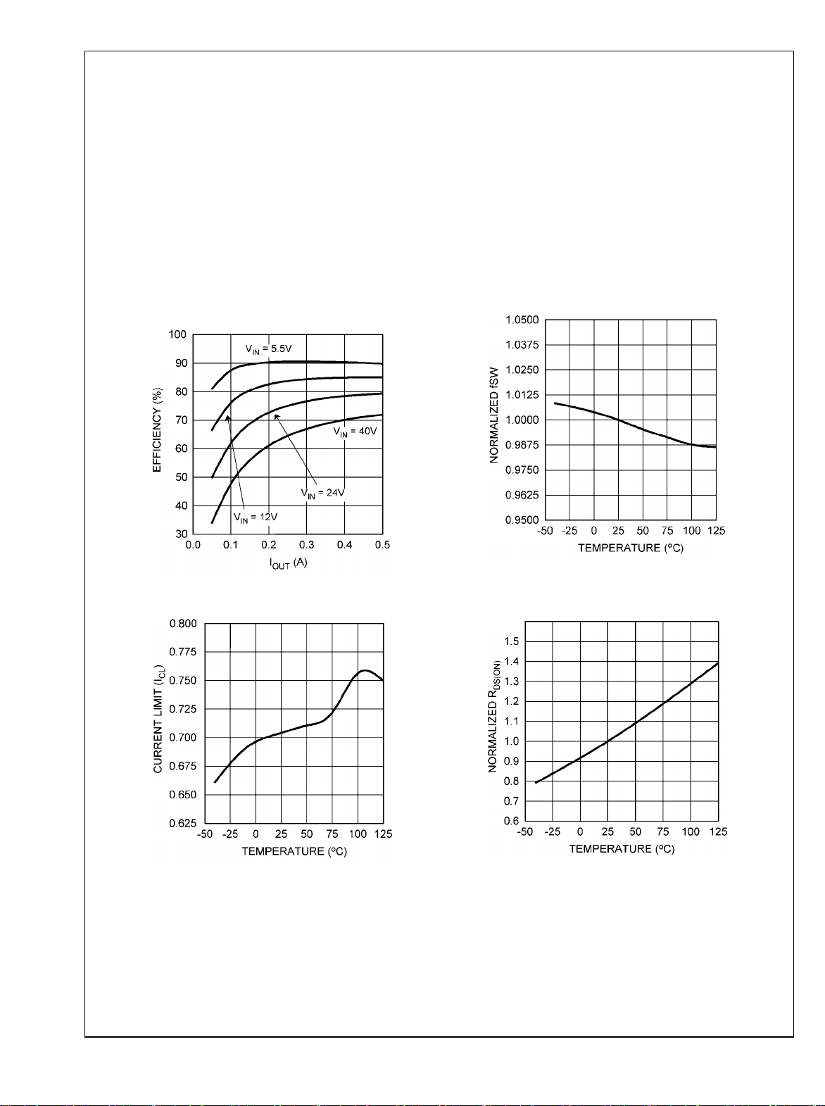
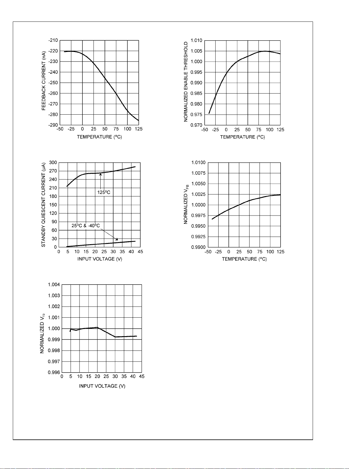
Typical Performance Characteristics Unless otherwise specified the following conditions apply: Vin =
12V, TJ = 25°C.
Efficiency vs I
V
OUT
OUT
= 3.3V
and V
IN
Current Limit vs Temperature
30076927
Normalized Switching Frequency vs Temperature
30076904
Normalized R
vs Temperature
DS(ON)
30076903
www.national.com 4
30076908
LM22674
Feedback Bias Current vs Temperature
30076905
Standby Quiescent Current vs Input Voltage
Normalized Enable Threshold Voltage vs Temperature
30076910
Normalized Feedback Voltage vs Temperature
30076906
Normalized Feedback Voltage vs Input Voltage
30076909
30076907
5 www.national.com
 Loading...