

查询LM10BH供应商
LM10
Operational Amplifier and Voltage Reference
General Description
The LM10 series are monolithic linear ICs consisting of a
precision reference, an adjustable reference buffer and an
independent, high quality op amp.
The unit can operate from a total supply voltage as low as
1.1V or as high as 40V, drawing only 270µA. Acomplementary output stage swings within 15 mV of the supply terminals or will deliver
tion. Reference output can be as low as 200 mV.
The circuit is recommended for portable equipment and is
completely specified for operation from a single power cell.
In contrast, high output-drive capability, both voltage and
current, along with thermal overload protection, suggest it in
demanding general-purpose applications.
The device is capable of operating in a floating mode, independent of fixed supplies. It can function as a remote comparator, signal conditioner, SCR controller or transmitter for
±
20 mA output current with±0.4V satura-
LM10 Operational Amplifier and Voltage Reference
May 1998
analog signals, delivering the processed signal on the same
line used to supply power. It is also suited for operation in a
wide range of voltage- and current-regulator applications,
from low voltages to several hundred volts, providing greater
precision than existing ICs.
This series is available in the three standard temperature
ranges, with the commercial part having relaxed limits. In addition, a low-voltage specification (suffix “L”) is available in
the limited temperature ranges at a cost savings.
Features
n input offset voltage: 2.0 mV (max)
n input offset current: 0.7 nA (max)
n input bias current: 20 nA (max)
n reference regulation: 0.1%(max)
n offset voltage drift: 2µV/˚C
n reference drift: 0.002%/˚C
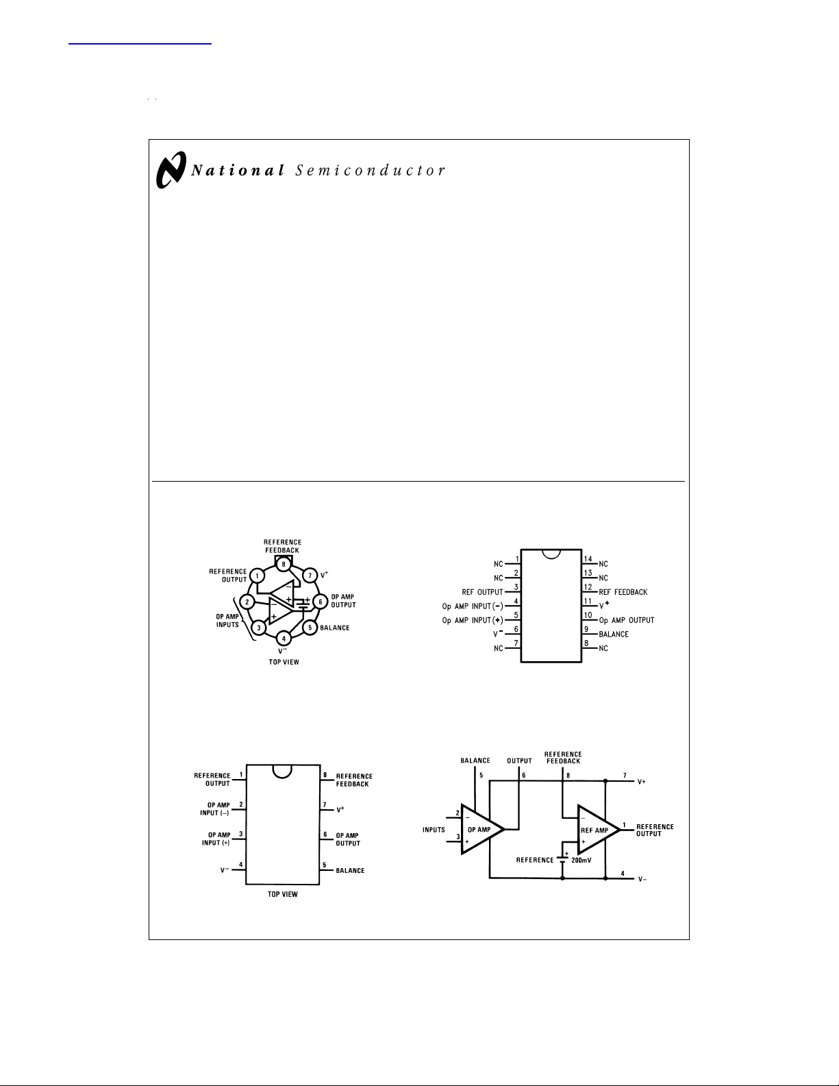
Connection and Functional Diagrams
Metal Can Package (H)
DS005652-1
Order Number LM10BH, LM10CH,
LM10CLH or LM10H/883
available per SMA
See NS Package Number H08A
Dual-In-Line Package (N)
Order Number LM10CN or LM10CLN
See NS Package Number N08E
#
5962-8760401
DS005652-15
Small Outline Package (WM)
DS005652-17
Order Number LM10CWM
See NS Package Number M14B
DS005652-16
© 1999 National Semiconductor Corporation DS005652 www.national.com
Absolute Maximum Ratings (Notes 1, 8)
If Military/Aerospace specified devices are required,
please contact the National Semiconductor Sales Office/
Distributors for availability and specifications.
LM10/LM10B/ LM10BL/
Total Supply Voltage 45V 7V
Differential Input Voltage (Note 2)
Power Dissipation (Note 3) internally limited
Output Short-circuit Duration (Note 4) continuous
Storage-Temp. Range −55˚C to +150˚C
Lead Temp. (Soldering, 10 seconds)
Metal Can 300˚C
Lead Temp. (Soldering, 10 seconds) DIP 260˚C
Vapor Phase (60 seconds) 215˚C
Infrared (15 seconds) 220˚C
LM10C LM10CL
±
40V
±
7V
ESD rating is to be determined.
Maximum Junction Temperature
LM10 150˚C
LM10B 100˚C
LM10C 85˚C
Operating Ratings
Package Thermal Resistance
θ
JA
H Package 150˚C/W
N Package 87˚C/W
WM Package 90˚C/W
θ
JC
H Package 45˚C/W
See AN-450 “Surface Mounting Methods and Their Effect on
Product Reliability” for other methods of soldering surface
mount devices.
Electrical Characteristics
=
T
25˚C, T
J
MIN≤TJ≤TMAX
Parameter Conditions LM10/LM10B LM10C Units
Input offset voltage 0.3 2.0 0.5 4.0 mV
Input offset current 0.25 0.7 0.4 2.0 nA
(Note 6) 1.5 3.0 nA
Input bias current 10 20 12 30 nA
Input resistance 250 500 150 400 kΩ
Large signal voltage V
gain V
Shunt gain (Note 7) 1.2V (1.3V) ≤V
Common-mode −20V≤V
rejection V
Supply-voltage −0.2V≥V
rejection V
Offset voltage drift 2.0 5.0 µV/˚C
Offset current drift 2.0 5.0 pA/˚C
Bias current drift T
Line regulation 1.2V (1.3V) ≤V
(Boldface type refers to limits over temperature range) (Note 5)
Min Typ Max Min Typ Max
3.0 5.0 mV
30 40 nA
150 115 kΩ
=
±
20V, I
S
=
OUT
=
±
V
20V, V
S
=
±
I
OUT
=
±
V
0.6V (0.65V), I
S
=
V
OUT
=
R
1.1 kΩ
L
0.1 mA≤I
1.5V≤V
0.1 mA≤I
=
±
20V 87 87 dB
S
+
=
1.0V (1.1V) 84 84 dB
1.0V (1.1V) ≤V
−
=
V
−0.2V 90 90 dB
<
100˚C 60 90 pA/˚C
C
0≤I
REF
=
0 120 400 80 400 V/mV
OUT
±
19.95V 80 50 V/mV
=
±
19.4V 50 130 25 130 V/mV
OUT
20 mA (±15 mA) 20 15 V/mV
=
±
2 mA 1.5 3.0 1.0 3.0 V/mV
OUT
±
0.4V (±0.3V), V
OUT
≤5mA 66V/mV
OUT
+
≤40V, R
L
≤20 mA 44V/mV
OUT
≤19.15V (19V) 93 102 90 102 dB
CM
−
≥−39V 90 96 87 96 dB
+
≤39.8V 96 106 93 106 dB
≤40V 0.001 0.003 0.001 0.008
S
≤1.0 mA, V
=
−0.4V 0.5 0.75 V/mV
CM
≤40V, 14 33 10 33 V/mV
=
250Ω 8 25 6 25 V/mV
=
200 mV 0.006 0.01
REF
%
/V
%
/V
www.national.com 2
Electrical Characteristics (Continued)
=
T
25˚C, T
J
MIN≤TJ≤TMAX
(Boldface type refers to limits over temperature range) (Note 5)
Parameter Conditions LM10/LM10B LM10C Units
Min Typ Max Min Typ Max
Load regulation 0≤I
REF
+
V
−V
Amplifier gain 0.2V≤V
≤1.0 mA 0.01 0.1 0.01 0.15
≥1.0V (1.1V) 0.15 0.2
REF
≤35V 50 75 25 70 V/mV
REF
%
%
23 15 V/mV
Feedback sense 195 200 205 190 200 210 mV
voltage 194 206 189 211 mV
Feedback current 20 50 22 75 nA
65 90 nA
Reference drift 0.002 0.003
%
/˚C
Supply current 270 400 300 500 µA
500 570 µA
Supply current change 1.2V (1.3V) ≤V
≤40V 15 75 15 75 µA
S
Electrical Characteristics
=
T
25˚C, T
J
MIN≤TJ≤TMAX
Parameter Conditions LM10BL LM10CL Units
Input offset voltage 0.3 2.0 0.5 4.0 mV
Input offset current 0.1 0.7 0.2 2.0 nA
(Note 6) 1.5 3.0 nA
Input bias current 10 20 12 30 nA
Input resistance 250 500 150 400 kΩ
Large signal voltage V
gain V
Shunt gain (Note 7) 1.5V≤V
Common-mode −3.25V≤V
rejection V
Supply-voltage −0.2V≥V
rejection V
Offset voltage drift 2.0 5.0 µV/˚C
Offset current drift 2.0 5.0 pA/˚C
Bias current drift 60 90 pA/˚C
Line regulation 1.2V (1.3V) ≤V
Load regulation 0≤I
(Boldface type refers to limits over temperature range) (Note 5)
Min Typ Max Min Typ Max
3.0 5.0 mV
30 40 nA
150 115 kΩ
=
±
3.25V, I
S
=
±
OUT
=
±
V
3.25V, I
S
=
±
V
OUT
=
±
V
0.6V (0.65V), I
S
=
±
V
OUT
+
0.1 mA≤I
=
±
3.25V 83 74 dB
S
+
=
1.0V (1.2V) 80 74 dB
1.0V (1.1V) ≤V
−
=
V
0.2V 88 74 dB
0≤I
≤0.5 mA, V
REF
≤0.5 mA 0.01 0.1 0.01 0.15
REF
+
V
−V
REF
=
0 60 300 40 300 V/mV
OUT
3.2V 40 25 V/mV
=
10 mA 10 25 5 25 V/mV
OUT
2.75 V 43V/mV
=
±
2 mA 1.5 3.0 1.0 3.0 V/mV
OUT
0.4V (±0.3V), V
≤6.5V, R
L
≤10 mA 44V/mV
OUT
≤2.4V (2.25V) 89 102 80 102 dB
CM
−
≥−5.4V 86 96 80 96 dB
+
≤6.3V 94 106 80 106 dB
≤6.5V 0.001 0.01 0.001 0.02
S
=
−0.4V 0.5 0.75 V/mV
CM
=
500Ω 8 30 6 30 V/mV
=
200 mV 0.02 0.03
REF
≥1.0V (1.1V) 0.15 0.2
%
/V
%
/V
%
%
www.national.com3
Electrical Characteristics (Continued)
=
T
25˚C, T
J
MIN≤TJ≤TMAX
Parameter Conditions LM10BL LM10CL Units
Amplifier gain 0.2V≤V
Feedback sense voltage 195 200 205 190 200 210 mV
Feedback current 20 50 22 75 nA
Reference drift 0.002 0.003
Supply current 260 400 280 500 µA
Note 1: Absolute Maximum Ratings indicate limits beyond which damage to the device may occur. Operating Ratings indicate conditions for which the device is functional, but do not guarantee specific performance limits.
Note 2: The Input voltage can exceed the supply voltages provided that the voltage from the input to any other terminal does not exceed the maximum differential
input voltage and excess dissipation is accounted for when V
Note 3: The maximum, operating-junction temperature is 150˚C for the LM10, 100˚C for the LM10B(L) and 85˚C for the LM10C(L). At elevated temperatures, devices
must be derated based on package thermal resistance.
Note 4: Internal thermal limiting prevents excessive heating that could result in sudden failure, but the IC can be subjected to accelerated stress with a shorted output
and worst-case conditions.
Note 5: These specifications apply for V
for the standard part and 6.5V for the low voltage part. Normal typeface indicates 25˚C limits. Boldface type indicates limits and altered test conditions for
full-temperature-range operation; this is −55˚C to 125˚C for the LM10, −25˚C to 85˚C for the LM10B(L) and 0˚C to 70˚C for the LM10C(L). The specifications do
not include the effects of thermal gradients (τ
curves).
Note 6: For T
Note 7: This defines operation in floating applications such as the bootstrapped regulator or two-wire transmitter. Output is connected to the V
and input common mode is referred to V
the positive-supply rejection error.
Note 8: Refer to RETS10X for LM10H military specifications.
>
90˚C, IOSmay exceed 1.5 nA for V
J
(Boldface type refers to limits over temperature range) (Note 5)
Min Typ Max Min Typ Max
≤5.5V 30 70 20 70 V/mV
REF
20 15 V/mV
194 206 189 211 mV
65 90 nA
500 570 µA
<
V−.
IN
−
≤VCM≤V+−0.85V (1.0V), 1.2V (1.3V)<VS≤V
≅
20 ms), die heating (τ
1
=
V
CM
−
(see typical applications). Effect of larger output-voltage swings with higher load resistance can be accounted for by adding
−
. With T
≅
0.2s) or package heating. Gradient effects are small and tend to offset the electrical error (see
2
=
125˚C and V
J
−
≤VCM≤V−+0.1V, IOS≤5 nA.
MAX,VREF
=
0.2V and 0≤I
≤1.0 mA, unless otherwise specified: V
REF
MAX
+
terminal of the IC
%
=
40V
/˚C
Definition of Terms
Input offset voltage: That voltage which must be applied
between the input terminals to bias the unloaded output in
the linear region.
Input offset current: The difference in the currents at the input terminals when the unloaded output is in the linear region.
Input bias current: The absolute value of the average of the
two input currents.
Input resistance: The ratio of the change in input voltage to
the change in input current on either input with the other
grounded.
Large signal voltage gain: The ratio of the specified output
voltage swing to the change in differential input voltage required to produce it.
Shunt gain: The ratio of the specified output voltage swing
to the change in differential input voltage required to produce
it with the output tied to the V
and power source are connected between the V
minals, and input common-mode is referred to the V
nal.
Common-mode rejection: The ratio of the input voltage
range to the change in offset voltage between the extremes.
www.national.com 4
+
terminal of the IC. The load
+
and V−ter-
−
termi-
Supply-voltage rejection: The ratio of the specified
supply-voltage change to the change in offset voltage between the extremes.
Line regulation: The average change in reference output
voltage over the specified supply voltage range.
Load regulation: The change in reference output voltage
from no load to that load specified.
Feedback sense voltage: The voltage, referred to V
−
,on
the reference feedback terminal while operating in regulation.
Reference amplifier gain: The ratio of the specified reference output change to the change in feedback sense voltage
required to produce it.
Feedback current: The absolute value of the current at the
feedback terminal when operating in regulation.
Supply current: The current required from the power
source to operate the amplifier and reference with their outputs unloaded and operating in the linear range.
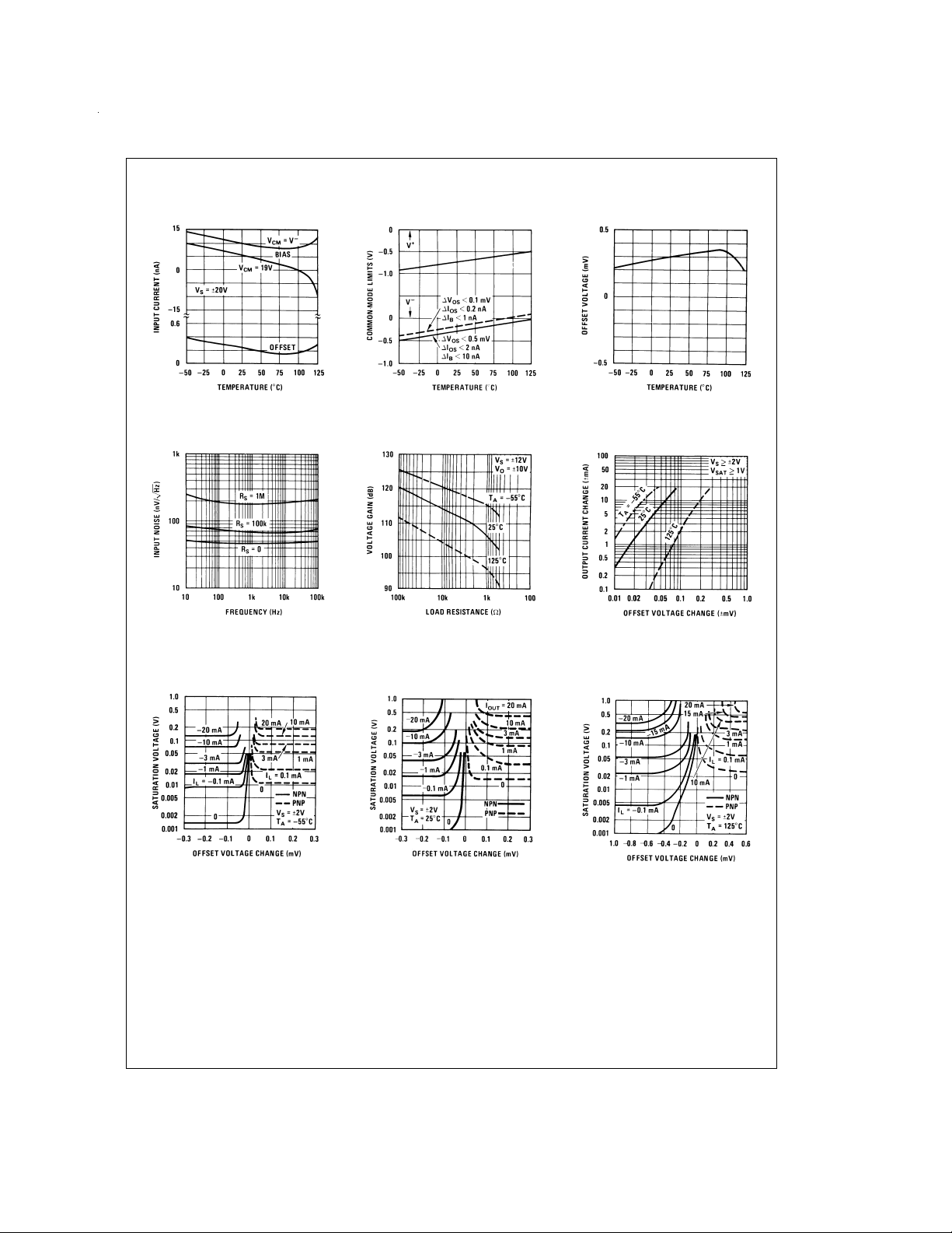
Typical Performance Characteristics (Op Amp)
Input Current
Input Noise Voltage
DS005652-18
DS005652-21
Common Mode Limits
DC Voltage Gain
DS005652-19
DS005652-22
Output Voltage Drift
DS005652-20
Transconductance
DS005652-23
Output Saturation
Characteristics
DS005652-24
Output Saturation
Characteristics
DS005652-25
Output Saturation
Characteristics
DS005652-26
www.national.com5
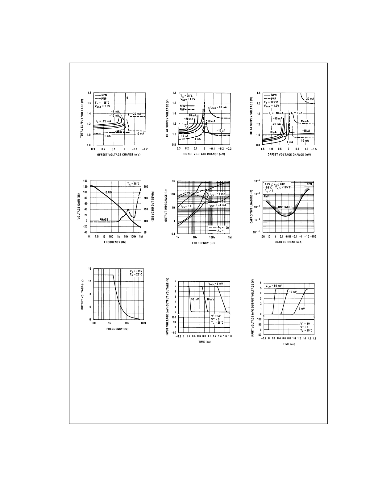
Typical Performance Characteristics (Op Amp) (Continued)
Minimum Supply Voltage
Frequency Response
Large Signal Response
DS005652-27
DS005652-30
Minimum Supply Voltage
Output Impedance
Comparator Response
Time For Various
Input Overdrives
DS005652-28
DS005652-31
Minimum Supply Voltage
DS005652-29
Typical Stability Range
DS005652-32
Comparator Response
Time For Various
Input Overdrives
DS005652-33
www.national.com 6
DS005652-34
DS005652-35
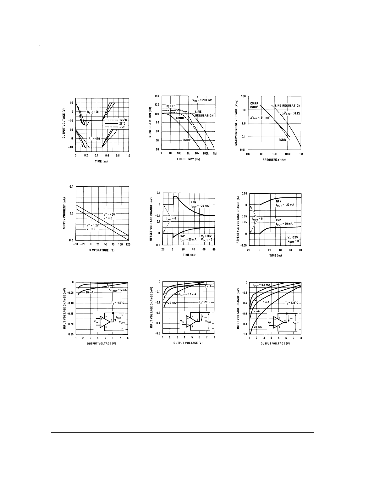
Typical Performance Characteristics (Op Amp) (Continued)
Follower Pulse
Response
Supply Current
DS005652-36
DS005652-39
Noise Rejection
Thermal Gradient
Feedback
DS005652-37
DS005652-40
Rejection Slew Limiting
DS005652-38
Thermal Gradient
Cross-coupling
DS005652-41
Shunt Gain
DS005652-42
Shunt Gain
DS005652-43
Shunt Gain
DS005652-44
www.national.com7
 Loading...