

February 2002
DS92LV16
16-Bit Bus LVDS Serializer/Deserializer - 25 - 80 MHz
DS92LV1616-Bit Bus LVDS Serializer/Deserializer - 25 - 80 MHz
General Description
The DS92LV16Serializer/Deserializer(SERDES)pairtransparently translates a 16–bit parallel bus into a BLVDS serial
stream with embedded clock information. This single serial
stream simplifies transferring a 16-bit, or less bus over PCB
traces andcablesby eliminating the skew problems between
parallel data and clock paths. It saves system cost by narrowing data paths that in turn reduce PCB layers, cable
width, and connector size and pins.
This SERDES pair includes built-in system and device test
capability. The line loopback and local loopback features
provide the following functionality: the local loopback enables the user to check the integrity of the transceiver from
the local parallel-bus side and the system can check the
integrity of the data transmission line by enabling the line
loopback.
The DS92LV16 incorporates BLVDS signaling on the highspeed I/O. BLVDS provides a low power and low noise
environment for reliably transferring data over a serial transmission path. The equal and opposite currents through the
differential data path control EMI by coupling the resulting
fringing fields together.
Block Diagram
DS92LV16
Features
n 25–80 MHz 16:1/1:16 serializer/deserializer (2.56Gbps
full duplex throughput)
n Independent transmitter and receiver operation with
separate clock, enable, power down pins
n Hot plug protection (power up high impedance) and
synchronization (receiver locks to random data)
n Wide +/−5% reference clock frequency tolerance for
easy system design using locally-generated clocks
n Line and local loopback modes
n Robust BLVDS serial transmission across backplanes
and cables for low EMI
n No external coding required
n Internal PLL, no external PLL components required
n Single +3.3V power supply
n Low power: 104mA (typ) transmitter, 119mA (typ)
receiver at 80MHz
±
n
100mV receiver input threshold
n Loss of lock detection and reporting pin
n Industrial −40 to +85˚C temperature range
>
n
2.5kV HBM ESD
n Compact, standard 80-pin PQFP package
20014301
© 2002 National Semiconductor Corporation DS200143 www.national.com
Absolute Maximum Ratings (Note 1)
If Military/Aerospace specified devices are required,
please contact the National Semiconductor Sales Office/
DS92LV16
Distributors for availability and specifications.
Supply Voltage (V
LVCMOS/LVTTL Input
Voltage −0.3V to (V
) −0.3V to +4V
CC
CC
+0.3V)
Maximum Package Power Dissipation Capacity
Package Derating:
23.2 mW/˚C above
80L PQFP
θ
JA
θ
JC
ESD Rating (HBM)
+25˚C
43˚C/W
11.1˚C/W
>
LVCMOS/LVTTL Output
Voltage −0.3V to (V
Bus LVDS Receiver Input
Voltage −0.3V to +3.9V
Bus LVDS Driver Output
Voltage −0.3V to +3.9V
Bus LVDS Output Short
Circuit Duration 10ms
Junction Temperature +150˚C
Storage Temperature −65˚C to +150˚C
CC
+0.3V)
Recommended Operating Conditions
Min Nom Max Units
Supply Voltage (V
Operating Free Air
Temperature (T
Clock Rate 25 80 MHz
) 3.15 3.3 3.45 V
CC
)
A
−40 +25 +85 ˚C
Lead Temperature
(Soldering, 4 seconds) +260˚C
Electrical Characteristics
Over recommended operating supply and temperature ranges unless otherwise specified.
Symbol Parameter Conditions Pin/Freq. Min Typ Max Units
LVCMOS/LVTTL DC Specifications
V
IH
V
IL
V
CL
I
IN
V
OH
V
OL
I
OS
I
OZ
Bus LVDS DC specifications
VTH
VTL
I
IN
High Level Input Voltage 2.0 V
Low Level Input Voltage
TCLK_R/F,DEN,
TCLK, TPWDN, DIN,
GND 0.8 V
SYNC, RCLK_R/F,
Input Clamp Voltage ICL= −18 mA
REN, REFCLK,
-0.7 −1.5 V
PWRDN
Input Current VIN= 0V or 3.6V −10
±
2 +10 µA
High Level Output Voltage IOH= −9 mA 2.3 3.0 V
Low Level Output Voltage IOL=9mA R
, RCLK, LOCK GND 0.33 0.5 V
OUT
Output Short Circuit Current VOUT = 0V −15 −48 −85 mA
PWRDN or REN =
TRI-STATE Output Current
0.8V, V
OUT
=0Vor
R
, RCLK, −10
OUT
±
0.4 +10 µA
VCC
Differential Threshold High
Voltage
Differential Threshold Low
Voltage
Input Current
VCM = +1.1V +100 mV
RI+, RI- −100 mV
= +2.4V, VCC=
V
IN
3.6V or 0V
= 0V, VCC= 3.6V
V
IN
or 0V
−10
−10
±
5 +10 µA
±
5 +10 µA
2.5kV
CC
CC
V
V
www.national.com 2

Electrical Characteristics (Continued)
Over recommended operating supply and temperature ranges unless otherwise specified.
Symbol Parameter Conditions Pin/Freq. Min Typ Max Units
V
OD
∆V
OD
V
OS
∆V
OS
I
OS
I
OZ
I
OX
SER/DES SUPPLY CURRENT (DVDD, PVDD and AVDD pins)
I
CCT
I
CCX
Output Differential Voltage
(DO+) - (DO-)
Output Differential Voltage
Unbalance
RL = 100Ω,
Figure 17
350 500 550 mV
215mV
Offset Voltage 1.05 1.2 1.25 V
Offset Voltage Unbalance 2.7 15 mV
Output Short Circuit Current
DO = 0V, Din = H,
TXPWDN and DEN =
DO+, DO-
-35 -50 -70 mA
2.4V
TXPWDN or DEN =
Tri-State Output Current
0.8V, DO = 0V OR
-10
±
110µA
VDD
Power-Off Output Current
Total Supply Current (includes
load current)
VDD = 0V, DO = 0V
or 3.6V
= 15 pF, RL= 100Ωf = 80 MHz, PRBS15
C
L
pattern
f = 80 MHz, Worse
= 15 pF, RL= 100
C
L
Ω
case pattern
(Checker-board
-10
±
110µA
209 mA
225 320 mA
pattern)
Supply Current Powerdown
PWRDN = 0.8V,
REN = 0.8V
0.35 1.0 mA
DS92LV16
Serializer Timing Requirements for TCLK
Over recommended operating supply and temperature ranges unless otherwise specified.
Symbol Parameter Conditions Min Typ Max Units
t
TCP
t
TCIH
t
TCIL
t
CLKT
t
JIT
Transmit Clock Period 12.5 T 40 ns
Transmit Clock High Time 0.4T 0.5T 0.6T ns
Transmit Clock Low Time 0.4T 0.5T 0.6T ns
TCLK Input Transition
Time
TCLK Input Jitter 80
36ns
ps
(RMS)
Serializer Switching Characteristics
Over recommended operating supply and temperature ranges unless otherwise specified.
Symbol Parameter Conditions Min Typ Max Units
t
LLHT
t
LHLT
t
t
DIS
DIH
Bus LVDS Low-to-High
Transition Time
Bus LVDS High-to-Low
Transition Time
DIN (0-15) Setup to TCLK
DIN (0-15) Hold from
TCLK
= 100Ω
R
L
Figure 3
CL=10pF to GND
Figure 6
RL= 100Ω,
=10pF to GND
C
L
2.4 ns
0ns
0.2 0.4 ns
0.2 0.4 ns
www.national.com3
Serializer Switching Characteristics (Continued)
Over recommended operating supply and temperature ranges unless otherwise specified.
Symbol Parameter Conditions Min Typ Max Units
DS92LV16
t
t
t
t
t
t
t
t
HZD
LZD
ZHD
ZLD
SPW
PLD
t
SD
RJIT
DJIT
DO±HIGH to
TRI-STATE Delay
DO±LOW to
TRI-STATE Delay
DO±TRI-STATE to
HIGH Delay
Figure 7
C
(Note 4)
= 100Ω,
R
L
=10pF to GND
L
DO±TRI-STATE to
LOW Delay
SYNC Pulse Width
Serializer PLL Lock Time 510*t
Serializer Delay
Figure 8
RL= 100Ω
Figure 9
RL= 100Ω t
5*t
TCP
TCP
TCP
+ 1.0 t
2.3 10 ns
1.9 10 ns
1.0 10 ns
1.0 10 ns
6*t
TCP
513*t
TCP
+ 2.0 t
TCP
+ 4.0 ns
TCP
Random Jitter 10 ps(rms)
Deterministic Jitter
Figure 15
35 MHz -240 140 ps
80 MHz -75 100 ps
Deserializer Timing Requirements for REFCLK
Over recommended operating supply and temperature ranges unless otherwise specified.
Symbol Parameter Conditions Min Typ Max Units
t
RFCP
t
RFDC
t
RFCP
t
t
RFTT
/
TCP
REFCLK Period 12.5 T 40 ns
REFCLK Duty Cycle 40 50 60 %
Ratio of REFCLK to
TCLK
0.95 1.05
REFCLK Transition Time 6ns
ns
ns
Deserializer Switching Characteristics
Over recommended operating supply and temperature ranges unless otherwise specified.
Symbol Parameter Conditions Pin/Freq. Min Typ Max Units
t
t
Receiver out Clock
RCP
RDC
RCLK Duty Cycle RCLK 45 50 55 %
Period
CMOS/TTL
t
CLH
Low-to-High
Transition Time
CMOS/TTL
t
CHL
High-to-Low
Transition Time
t
t
t
t
t
t
ROUT (0-9) Setup
ROS
ROH
HZR
LZR
ZHR
ZLR
t
DD
Data to RCLK
ROUT (0-9) Hold
Data to RCLK
HIGH to TRI-STATE
Delay
LOW to TRI-STATE
Delay
TRI-STATE to HIGH
Delay
TRI-STATE to LOW
Delay
Deserializer Delay RCLK
Figure 9
t
RCP=tTCP
CL=15pF
Figure 4
Figure 11
Figure 12
RCLK 12.5 40 ns
24ns
Rout(0-9),
LOCK,
24ns
RCLK
0.35*t
−0.35*t
RCP
RCP
0.5*t
−0.5*t
RCP
RCP
2.2 10 ns
Rout(0-9),
LOCK
2.2 10 ns
2.3 10 ns
2.9 10 ns
1.75*t
+2
RCP
1.75*t
+ 5 1.75*t
RCP
+7 ns
RCP
ns
ns
www.national.com 4
Deserializer Switching Characteristics (Continued)
Over recommended operating supply and temperature ranges unless otherwise specified.
Symbol Parameter Conditions Pin/Freq. Min Typ Max Units
Deserializer PLL
t
DSR1
Lock Time from
PWRDWN (with
SYNCPAT)
(Note 7)
Deserializer PLL
t
DSR2
Lock time from
SYNCPAT
t
RNMI-R
t
RNMI-L
Note 1: “Absolute Maximum Ratings” are those values beyond which the safety of the device cannot be guaranteed. They are not meant to imply that the devices
should be operated at these limits. The table of “Electrical Characteristics” specifies conditions of device operation.
Note 2: Typical values are given for V
Note 3: Current into device pins is defined as positive. Current out of device pins is defined as negative. Voltages are referenced to ground except VOD, ∆VOD,
VTH and VTL which are differential voltages.
Note 4: Due to TRI-STATE of the Serializer, the Deserializer will lose PLL lock and have to resynchronize before data transfer.
Note 5: For the purpose of specifying deserializer PLL performance tDSR1 and tDSR2 are specified with the REFCLK running and stable, and specific conditions
of the incoming data stream (SYNCPATs). It is recommended that the derserializer be initialized using either tDSR1 timing or tDSR2 timing. tDSR1 is the time
required for the deserializer to indicate lock upon power-up or when leaving the power-down mode. Synchronization patterns should be sent to the device before
initiating either condition. tDSR2 is the time required to indicate lock for the powered-up and enabled deserializer when the input (RI+ and RI-) conditions change
from not receiving data to receiving synchronization patterns (SYNCPATs).
Note 6: tRNMI is a measure of how much phase noise (jitter) the deserializer can tolerate in the incoming data stream before bit errors occur. It is a measurement
in reference with the ideal bit position, please see National’s AN-1217 for detail.
Note 7: Sync pattern is a fixed pattern with 8-bit of data high followed by 8-bit of data low.
Ideal Deserializer
Noise Margin Right
Ideal Deserializer
Noise Margin Left
Figure 16
(Note 6)
Figure 16
(Note 6)
= 3.3V and TA= +25˚C.
CC
35MHz 3.7 10 µs
80 MHz 1.9 4 µs
35MHz 1.5 5 µs
80 MHz 0.9 2 µs
35 MHz +630 ps
80 MHz +230 ps
35 MHz −630 ps
80 MHz −230 ps
DS92LV16
www.national.com5
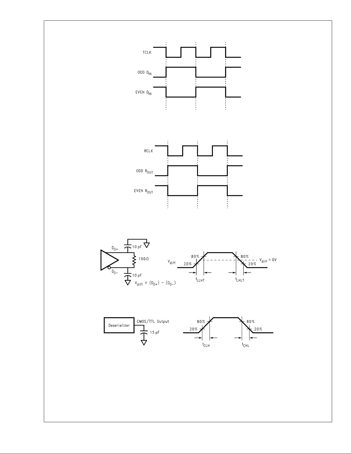
AC Timing Diagrams and Test Circuits
DS92LV16
FIGURE 1. “Worst Case” Serializer ICC Test Pattern
20014303
20014304
FIGURE 2. “Worst Case” Deserializer ICC Test Pattern
FIGURE 3. Serializer Bus LVDS Output Load and Transition Times
20014306
FIGURE 4. Deserializer CMOS/TTL Output Load and Transition Times
20014305
www.national.com 6

AC Timing Diagrams and Test Circuits (Continued)
FIGURE 5. Serializer Input Clock Transition Time
DS92LV16
20014307
20014308
FIGURE 6. Serializer Setup/Hold Times
20014309
FIGURE 7. Serializer TRI-STATE Test Circuit and Timing
www.national.com7

AC Timing Diagrams and Test Circuits (Continued)
DS92LV16
FIGURE 8. Serializer PLL Lock Time, SYNC Timing and PWRDN TRI-STATE Delays
20014310
FIGURE 9. Serializer Delay
FIGURE 10. Deserializer Delay
20014311
20014312
FIGURE 11. Deserializer Setup and Hold Times
www.national.com 8
20014313

AC Timing Diagrams and Test Circuits (Continued)
DS92LV16
FIGURE 12. Deserializer TRI-STATE Test Circuit and Timing
20014314
FIGURE 13. Deserializer PLL Lock Times and PWRDN TRI-STATE Delays
20014315
www.national.com9

AC Timing Diagrams and Test Circuits (Continued)
DS92LV16
FIGURE 14. Deserializer PLL Lock Time from SyncPAT
FIGURE 15. Deterministic Jitter and Ideal Bit Position
20014322
20014329
www.national.com 10

AC Timing Diagrams and Test Circuits (Continued)
DS92LV16
t
is the noise margin on the left of the above figure. It is a negative value to indicate early with respect to ideal.
RNMI-L
t
is the noise margin on the right of the above figure. It is a positive value to indicate late with respect to ideal.
RNMI-R
FIGURE 16. Deserializer Noise Margin (t
VOD= (DO+)–(DO−).
Differential output signal is shown as (DO+)–(DO−), device in Data Transfer mode.
) and Sampling window
RNMI
20014316
FIGURE 17. VODDiagram
20014332
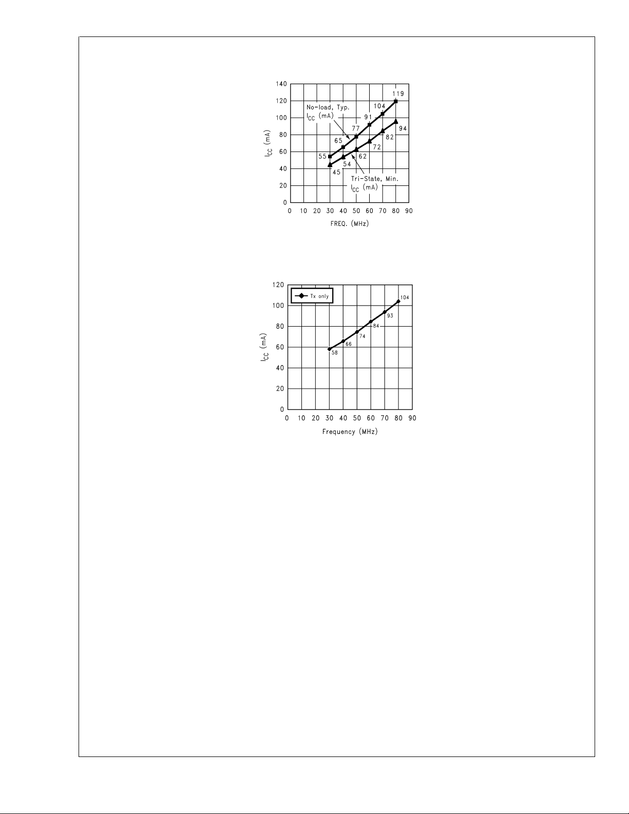
FIGURE 18. Icc vs Freq
20014323
www.national.com11
AC Timing Diagrams and Test Circuits (Continued)
DS92LV16
FIGURE 19. Icc vs Freq (Rx only)
20014324
20014325
FIGURE 20. Icc vs Freq (Tx only)
www.national.com 12

Functional Description
The DS92LV16 combines a serializer and deserializer onto a
single chip. The serializer accepts a 16-bit LVCMOS or
LVTTL data bus and transforms it into a BLVDS serial data
stream with embedded clock information. The deserializer
then recovers the clock and data to deliver the resulting
16-bit wide words to the output.
The device has a separate Transmitblock and Receive block
that can operate independent of each other. Each has a
power down control to enable efficient operation in various
applications. For example, the transceiver can operate as a
standby in a redundant data path but still conserve power.
The part can be configured as a Serializer, Deserializer, or
as a Full Duplex SER/DES.
The DS92LV16 serializer and deserializer blocks each has
three operating states. They are the Initialization, Data
Transfer, and Resynchronization states. In addition, there
are two passive states: Powerdown and TRI-STATE.
The following sections describe each operation mode and
passive state.
Initialization
Before the DS92LV16 sends or receives data, it must initialize the links to and from another DS92LV16. Initialization
refers to synchronizing the Serializer’s and Deserializer’s
PLL’s to local clocks. The local clocks must be the same
frequency or within a specified range if from different
sources. After the Serializers synchronizes to the local
clocks, the Deserializers synchronize to the Serializers as
the second and final initialization step.
Step 1: When V
rializer, the respective outputs are held in TRI-STATE and
internal circuitry is disabled by on-chip power-on circuitry.
When V
begins locking to a local clock. For the Serializer, the local
clock is the transmit clock, TCLK. For the Deserializer, the
local clock is applied to the REFCLK pin. A local on-board
oscillator or other source provides the specified clock input
to the TCLK and REFCLK pin.
The Serializer outputs are held in TRI-STATE while the PLL
locks to the TCLK. After locking to TCLK, the Serializer block
is now ready to send data or synchronization patterns. If the
SYNC pin is high, then the Serializer block generates and
sends the synchronization patterns (sync-pattern).
The Deserializer output will remain TRI-STATE while its PLL
locks to the REFCLK.Also, the Deserializer LOCK output will
remain high until its PLL locks to an incoming data or syncpattern on the RIN pins.
Step 2: The Deserializer PLL must synchronize to the Serializer to complete the initialization. The Serializer that is
generating the stream to the Deserializer must send random
(non-repetitive) data patterns or sync-patterns during this
step of the Initialization State. The Deserializer will lock onto
sync-patterns within a specified amount of time. The lock to
random data depends on the data patterns and therefore,
the lock time is unspecified.
In order to lock to the incoming LVDS data stream, the
Deserializer identifies the rising clock edge in a sync-pattern
and after 150 clock cycles will synchronize. If the Deserializer is locking to a random data stream from the Serializer,
then it performs a series of operations to identify the rising
clock edge and locks to it. Because this locking procedure
depends on the data pattern, it is not possible to specify how
long it will take. At the point where the Deserializer’s PLL
CC
is applied to both Serializer and/or Dese-
CC
reaches VCCOK (2.2V) the PLL in each device
DS92LV16
locks to the embedded clock, the LOCK pin goes low and
valid data appears on the output. Note that the LOCK signal
is synchronous to valid data appearing on the outputs.
The user’s application determines whether sync-pattern or
lock to random data is the preferred method for synchronization. If sync-patterns are preferred, the associated deserializers LOCK pin is a convenient way to provide control of
the SYNC pin.
Data Transfer
After initialization, the DS92LV16 Serializer isable to transfer
data to the Deserializer. The serial data stream includes a
start bit and stop bit appended by the serializer,which frame
the sixteen data bits. The start bit is always high and the stop
bit is always low. The start and stop bits also function as
clock bits embedded in the serial stream.
The Serializer block accepts data from the DIN0-DIN15 parallel inputs. The TCLK signal latches the incoming data on
the rising edge. If the SYNC input is high for 6 TCLK cycles,
the DS92LV16 does not latch data on the DIN0-DIN15.
The Serializer transmits the data and clock bits (16+2 bits) at
18 times the TCLK frequency. For example, if TCLK is 60
MHz, the serial rate is 60 X 18 = 1080 Mbps. Since only 16
bits are from input data, the serial ’payload’ rate is 16 times
the TCLK frequency. For instance, if TCLK = 60 MHz, the
payload data rate is 60 X 16 = 960 Mbps. TCLK is provided
by the data source and must be in the range of 25 MHz to 80
MHz.
When the Deserializer channel synchronizes to the input
from a Serializer, it drives its LOCK pin low and synchronously delivers valid data on the output. The Deserializer
locks to the embedded clock, uses it to generate multiple
internal data strobes, and then drives the recovered clock on
the RCLK pin. The RCLK is synchronous to the data on the
ROUT[0:15] pins. While LOCK is low, data on ROUT[0:15] is
valid. Otherwise, ROUT[0:15] is invalid.
ROUT[0:15], LOCK, and RCLK signals will drive a minimum
of three CMOS input gates (15pF total load) at a 80 MHz
clock rate. This drive capacity allows bussing outputs of
multiple Deserializers and multiple destination ASIC inputs.
REN controls TRI-STATE of the all outputs.
The Deserializer input pins are high impedance during Receiver Powerdown (RPWDN* low) and power-off (VCC =
0V).
Resynchronization
Whenever the Deserializer loses lock, it will automatically try
to resynchronize. For example, if the embedded clock edge
is not detected two times in succession, the PLL loses lock
and the LOCK pin is driven high. The Deserializer then
enters the operating mode where it tries to lock to random a
data stream. It looks for the embedded clock edge, identifies
it and then proceeds through the synchronization process.
The logic state of the LOCK signal indicates whether the
data on ROUT is valid; when it is low, the data is valid. The
system must monitor the LOCK pin to determine whether
data on the ROUT is valid. Because there is a short delay in
the LOCK signals response to the PLL losing synchronization to the incoming data stream, the system must determine
the validity of data for the cycles before the LOCK signal
goes high.
www.national.com13

Resynchronization (Continued)
The user can choose to resynchronize to the random data
stream or to force fast synchronization by pulsing the Seri-
DS92LV16
alizer SYNC pin. Since lock time varies due to data stream
characteristics, we cannot possibly predict exact lock time.
The primary constraint on the ’random’ lock time is the initial
phase relation between the incoming data and the REFCLK
when the Deserializer powers up. An advantage of using the
SYNC pattern to force synchronization is the ability for user
to predict the delay for PLL to regain lock. This scheme is left
up to the user discretion. One recommendation is to provide
a feedback loop using the LOCK pin itself to control the sync
request of the Serializer, which is the SYNC pin.
If a specific pattern is repetitive, the Deserializer’s PLL will
not lock in order to prevent the Deserializer to lock to the
data pattern rather than the clock. We refer to such pattern
as a repetitive multi-transition, RMT. This occurs when more
than one Low-High transition takes places in a clock cycle
over multiple cycles. This occurs when any bit, except DIN
15, is held at a low state and the adjacent bit is held high,
creating a 0-1 transition. The internal circuitry accomplishes
this by detecting more than one potential position for clocking bits. Upon detection, the circuitry will prevent the LOCK
output from becoming active until the RMT pattern changes.
Once the RMT pattern changes and the internal circuitry
recognized the clock bits in the serial data stream, the PLLof
the Deserializer will lock, which will drive the LOCK output to
low and the output data ROUT will become valid.
Powerdown
The Powerdown state is a low power sleep mode that the
Serializer and Deserializer will occupy while waiting for initialization. You can also use TPWDN* and RPWDN* to reduce power when there are no pending data transfers. The
Deserializer enters Powerdown when RPWDN* is driven
low. In Powerdown, the PLL stops and the outputs go into
TRI-STATE, which reduces supply current to the µA range.
To bring the Deserializer block out of the Powerdown state,
the system drives RPWDN* high. When the Deserializer
exits Powerdown, it automatically enters the Initialization
state. The system must then allow time for Initialization
before data transfer can begin.
The TPWDN* driven to a low condition forces the Serializer
block into low power consumption where the supply current
is in the µA range. The Serializer PLL stops and the output
goes into a TRI-STATE condition.
To bring the Serializer block out of the Powerdown state, the
system drives TPWDN* high. When the Serializer exits Powerdown, its PLL must lock the TCLK before it is ready for the
Initialization state. The system must then allow time for
Initialization before data transfer can begin.
TRI-STATE
When the system drives the REN pin low, the Deserializer
output enter TRI-STATE. This will TRI-STATE the receiver
output pins (ROUT[0:15]) and RCLK. When the system
drives REN high, the Deserilaizer will return to the previous
state as long as all other control pins remain static (RPWDN*).
When the system drives the DEN pin low, the Serializer
output enters TRI-STATE. This will TRI-STATE the LVDS
output. When the system drives the DEN signal high, the
Serializer output will return to the previous state as long as
all other control and data input pins remain in the same
condition as when the DEN was driven low.
Loopback Test Operation
The DS92LV16 includes two Loopback modes for testing the
device functionality and the transmission line continuity. Asserting the Line Loopback control signal connects the serial
data input (RIN+/−) to the serial data output (DO+/−) and to
the parallel data output (ROUT[0:15]). The serial data goes
through deserializer and serializer blocks.
Asserting the Local Loopback control signal connects the
parallel data input (DIN[0:15]) back to the parallel data output (ROUT[0:15]). The connection route includes all the
functional blocks of the SER/DES Pair. The serial data output (DO+/−) is automatically disabled during the Local Loopback operating mode.
Application Information
Using the DS92LV16
The DS92LV16 combines a Serializer and a Deserializer into
a single chip that sends 16 bits of parallel TTL data over a
serial Bus LVDS link up to 1.28 Gbps. Serialization of the
input data is accomplished using an onboard PLL at the
Serializer which embeds two clock bits with the data. The
Deserializer uses a separate reference clock (REFCLK) and
an onboard PLL to extract the clock information from the
incoming data stream and deserialize the data. The Deserializer monitors the incoming clock information to determine
lock status and will indicate loss of lock by raising the LOCK
output.
Power Considerations
All CMOS design of the Serializer and Deserializer makes
them inherently low power devices.Additionally,the constant
current source nature of the LVDS outputs minimize the
slope of the speed vs. I
Powering Up the Deserializer
The REFCLK input can be running before the Deserializer is
powered up and it must be running in order for the Deserializer to lock to incoming data. The Deserializer outputs will
remain in TRI-STATE until the Deserializer detects data
transmission at its inputs and locks to the incoming stream.
Noise Margin
The Deserializer noise margin is the amount of input jitter
(phase noise) that the Deserializer can tolerate and still
reliably receive data. Various environmental and systematic
factors include:
Serializer: TCLK jitter, V
out-of-band noise)
Media: ISI, V
Deserializer: V
For typical receiver noise margin, please see
Recovering from LOCK Loss
In the case where the Serializer loses lock during data
transmission up to 5 cycles of data that was previously
received can be invalid. This is due to the delay in the lock
detection circuit. The lock detect circuit requires that invalid
clock information be received 2 times in a row to indicate
loss of lock. Since clock information has been lost it is
possible that data was also lost during these cycles. When
the Deserializer LOCK pin goes low, data from at least the
previous 5 cycles should be resent upon regaining lock.
CM
noise
CC
curve of CMOS designs.
CC
noise (noise bandwidth and
CC
noise
Figure 16
.
www.national.com 14

Application Information (Continued)
Lock can be regained at the Deserializer by causing the
Serializer to resend SYNC patterns as described above or
by random lock which can take more time depending upon
the data patterns being received.
Input Failsafe
In the event that the Deserializer is disconnected from the
Serializer, the failsafe circuitry is designed to reject certain
amount of noise from being interpreted as data or clock. The
outputs will be tri-stated and the Deserializer will lose lock.
Hot Insertion
All the LVDS devices are hot pluggable if you follow a few
rules. When inserting, ensure the Ground pin(s) makes contact first, then the VCC pin(s), then the I/O pins. When
removing, the I/O pins should be unplugged first, then the
VCC, then the Ground.
PCB Layout and Power System Considerations
Circuit board layout and stack-up for the BLVDS devices
should be designed to provide low-noise power feed to the
device. Good layout practice will also separate highfrequency or high-level inputs and outputs to minimize unwanted stray noise pickup, feedback and interference.
Power system performance may be greatly improved by
using thin dielectrics (2 to 4 mils) for power / ground sandwiches. This arrangement provides plane capacitance for
the PCB power system with low-inductance parasitic, especially proven effective at high frequencies above approx
50MHz, and makes the value and placement of external
bypass capacitors less critical. External bypass capacitors
should include both RF ceramic and tantalum electrolytic
types. RF capacitors may use values in the range of 0.01 uF
to 0.1 uF. Tantalum capacitors may be in the 2.2 uF to 10 uF
range. Voltagerating of the tantalum capacitors should be at
least 5X the power supply voltage being used.
It is a recommended practice to use two vias at each power
pin as well as at all RF bypass capacitor terminals. Dual vias
reduce the interconnect inductance by up to half, thereby
reducing interconnect inductance and extending the effective frequency range of the bypass components. Locate RF
capacitors as close as possible to the supply pins, and use
wide low impedance traces (not 50 Ohm traces). Surface
mount capacitors are recommended due to their smaller
parasitics. When using multiple capacitors per supply pin,
locate the smaller value closer to the pin. A large bulk
capacitor is recommend at the point of power entry. This is
typically in the 50uF to 100uF range and will smooth low
frequency switching noise. It is recommended to connect
power and ground pin straight to the power and ground
plane, with the bypass capacitors connected to the plane
with via on both ends of the capacitor. Connecting power or
ground pin to an external bypass capacitor will increase the
inductance of the path.
A small body size X7R chip capacitor, such as 0603, is
recommended for external bypass. Its small body size reduces the parasitic inductance of the capacitor. User must
pay attention to the resonance frequency of these external
bypass capacitors, usually in the range of 20-30MHz range.
To provide effective bypassing, very often, multiple capacitors are used to achieve low impedance between the supply
rails over the frequency of interest. At high frequency, it is
also a common practice to use two via from power and
ground pins to the planes, reducing the impedance at high
frequency.
DS92LV16
Some devices provide separate power and ground pins for
different portions of the circuit. This is done to isolate switching noise effects between different sections of the circuit.
Separate planes on the PCB are typically not required. Pin
Description tables typically provide guidance on which circuit
blocks are connected to which power pin pairs. In some
cases, an external filter many be used to provide clean
power to sensitive circuits such as PLLs.
Use at least a four layer board with a power and ground
plane. Locate CMOS (TTL) swings away from the LVDS
lines to prevent coupling from the CMOS lines to the LVDS
lines. Closely-coupled differential lines of 100 Ohms are
typically recommended for LVDS interconnect. The closelycoupled lines help to ensure that coupled noise will appear
as common-mode and thus is rejected by the receivers.Also
the tight coupled lines will radiate less.
Termination of the LVDS interconnect is required. For pointto-point applications termination should be located at the
load end. Nominal value is 100 Ohms to match the line’s
differential impedance. Place the resistor as close to the
receiver inputs as possible to minimize the resulting stub
between the termination resistor and receiver.
Additional general guidance can be found in the LVDSOwner’s Manual - available in PDF format from the national web
site at: www.national.com/lvds
Specific guidance for this device is provided next:
DS92LV16 BLVDS SER/DES PAIR
General device specific guidance is given below. Exact guidance can not be given as it is dictated by other board level
/system level criteria. This includes the density of the board,
power rails, power supply,and other integrated circuit power
supply needs.
DVDD = Digital section power supply
These pins supply the digital portion of the device and also
receiver output buffers. TheTX DVDD is less critical. The RX
DVDD requires more bypass to power the outputs under
synchronous switching conditions. The receiver DVDD pins
power 4 outputs from each DVDD pin. An estimate of local
capacitance required indicates a minimum of 22nF is required. This is calculated by taking 4 times the maximum
short current (4 X 70 = 280mA) multiplying by the rise time of
the part (4ns) and dividing by the maximum allowed droop in
VDD (assume 50mV) yields 22.4nF. Rounding up to a standard value, 0.1uF is selected for each DVDD pin.
PVDD = PLL section power supply
The PVDD pin supplies the PLL circuit. Note that the
DS92LV16 has two separate PLLs and supply pins. The
PLL(s) require clean power for the minimization of Jitter. A
supply noise frequency in the 300kHZ to 1MHz range can
cause increased output jitter. Certain power supplies may
have switching frequencies or high harmonic content in this
range. If this is the case, filtering of this noise spectrum may
be required. A notch filter response is best to provide a stable
VDD, suppression of the noise band, and good highfrequency response (clock fundamental). This may be accomplished with a pie filter (CRC or CLC). If employed, a
separate pie filter is recommended for each PLL to minimize
drop in potential due to the series resistance. The pie filter
should be located close to the PVDD power pin. Separate
power planes for the PVDD pins is typically not required.
AVDD = LVDS section power supply
The AVDD pin supplies the LVDS portion of the circuit. The
DS92LV16 has four AVDD pins. Due to the nature of the
design, current draw is not excessive on these pins. A0.1uF
www.national.com15

Application Information (Continued)
capacitor is sufficient for these pins. If space is available it
0.01uF may be used in parallel with the 0.1uF capacitor for
DS92LV16
additional high frequency filtering.
GROUNDs
TheAGND pin should be connected to the signal common in
the cable for the return path of any common-mode current.
Most of the LVDS current will be odd-mode and return within
the interconnect pair. A small amount of current may be
even-mode due to coupled noise, and driver imbalances.
This current should return via a low impedance known path.
Asolid ground plane is recommended for both DVDD, PVDD
or AVDD. Using a split plane may have potential problem of
ground loops, or difference in ground potential at various
ground pins of the device.
www.national.com 16

Pin Diagram
DS92LV16
DS92LV16TVHG
Top VIew
20014302
www.national.com17

Pin Descriptions
DS92LV16
Pin # Pin Name I/O Description
1 RPWDN* CMOS, I RPWDN* = Low will put the Receiver in low power, stand-by,
mode. Note: The Receiver PLL will lose lock.(Note 8)
2 REN CMOS, I REN = Low will disable the Receiver outputs. Receiver PLL
remains locked. (See LOCK pin description)(Note 8)
3 CONFIG1 Configuration pin - strap or tie this pin to High with pull-up resistor.
No-connect or Low reserved for future use.
4 REFCLK CMOS, I Frequency reference clock input for the receiver.
5, 10, 11, 15 AVDD Analog Voltage Supply
6,9,12,16 AGND Analog Ground
7 RIN+ LVDS, I Receiver LVDS True Input
8 RIN- LVDS, I Receiver LVDS Inverting Input
13 DO+ LVDS, O Transmitter LVDS True Output
14 DO- LVDS, O Transmitter LVDS Inverting Output
17 TCLK CMOS, I Transmitter reference clock. Used to strobe data at the DIN Inputs
and to drive the transmitter PLL. See TCLK Timing Requirements.
18 CONFIG2 Configuration pin - strap or tie this pin to High with pull-up resistor.
No-connect or Low reserved for future use.
19 DEN CMOS, I DEN = Low will disable the Transmitter outputs. The transmitter
PLL will remain locked.(Note 8)
20 SYNC CMOS, I SYNC = High will cause the transmitter to ignore the data inputs
and send SYNC patterns to provide a locking reference to
receiver(s). See Functional Description.(Note 8)
21, 22, 23, 24, 25, 26,
27, 28, 33, 34, 35, 36,
37, 38, 39, 40
29,32 PGND PLL Ground.
30,31 PVDD PLL Voltage supply.
41, 44, 51, 52, 59, 60,
61, 68, 80
42 TPWDN* CMOS, I TPWDN* = Low will put the Transmitter in low power, stand-by
43, 50, 53, 58, 62, 69 DVDD Digital Voltage Supplies.
45, 46, 47, 48, 54, 55,
56, 57, 64, 65, 66, 67,
70, 71, 72, 73
49 RCLK CMOS, O Recovered Clock. Parallel data rate clock recovered from
63 LOCK* CMOS, O LOCK* indicates the status of the receiver PLL. LOCK=H-
74,76 PGND PLL Grounds.
75,77 PVDD PLL Voltage Supplies.
78 LINE_LE CMOS, I LINE_LE = High enables the receiver loopback mode. Data
79 LOCAL_LE CMOS, I LOCAL_LE = High enables the transmitter loopback mode. Date
Note 8: Input defaults to ’low’ state when left open due to internal pull-device.
DIN (0:15) CMOS, I Transmitter data inputs.(Note 8)
DGND Digital Ground.
mode. Note: The transmitter PLL will lose lock.(Note 8)
ROUT (0:15) CMOS, O Receiver Outputs.
embedded clock. Used to strobe ROUT (0:15). LVCMOS Level
output.
receiver PLL is unlocked, LOCK=L-receiver PLL is locked.
received at the RIN+/- inputs is fed back through the DO+/outputs.(Note 8)
received at the DIN inputs is fed back through the ROUT
outputs.(Note 8)
www.national.com 18

Physical Dimensions inches (millimeters)
unless otherwise noted
DS92LV1616-Bit Bus LVDS Serializer/Deserializer - 25 - 80 MHz
Dimensions shown in millimeters only
Order Number DS92LV16TVHG
NS Package Number VHG80A
LIFE SUPPORT POLICY
NATIONAL’S PRODUCTS ARE NOT AUTHORIZED FOR USE AS CRITICAL COMPONENTS IN LIFE SUPPORT
DEVICES OR SYSTEMS WITHOUT THE EXPRESS WRITTEN APPROVAL OF THE PRESIDENT AND GENERAL
COUNSEL OF NATIONAL SEMICONDUCTOR CORPORATION. As used herein:
1. Life support devices or systems are devices or
systems which, (a) are intended for surgical implant
into the body, or (b) support or sustain life, and
whose failure to perform when properly used in
accordance with instructions for use provided in the
2. A critical component is any component of a life
support device or system whose failure to perform
can be reasonably expected to cause the failure of
the life support device or system, or to affect its
safety or effectiveness.
labeling, can be reasonably expected to result in a
significant injury to the user.
National Semiconductor
Corporation
Americas
Email: support@nsc.com
www.national.com
National does not assume any responsibility for use of any circuitry described, no circuit patent licenses are implied and National reserves the right at any time without notice to change said circuitry and specifications.
National Semiconductor
Europe
Fax: +49 (0) 180-530 85 86
Email: europe.support@nsc.com
Deutsch Tel: +49 (0) 69 9508 6208
English Tel: +44 (0) 870 24 0 2171
Français Tel: +33 (0) 1 41 91 8790
National Semiconductor
Asia Pacific Customer
Response Group
Tel: 65-2544466
Fax: 65-2504466
Email: ap.support@nsc.com
National Semiconductor
Japan Ltd.
Tel: 81-3-5639-7560
Fax: 81-3-5639-7507
 Loading...