

National Semiconductor DP8573A Technical data
DP8573A Real Time Clock (RTC)
DP8573A Real Time Clock (RTC)
May 1993
General Description
The DP8573A is intended for use in microprocessor based
systems where information is required for multi-tasking, data
logging or general time of day/date information. This device
is implemented in low voltage silicon gate microCMOS technology to provide low standby power in battery back-up environments. The circuit’s architecture is such that it looks
like a contiguous block of memory or I/O ports organized as
one block of 32 bytes. This includes the Control Registers,
the Clock Counters, the Alarm Compare RAM, and the Time
Save RAM.
Time and date are maintained from 1/100 of a second to
year and leap year in a BCD format, 12 or 24 hour modes.
Day of week and day of month counters are provided. Time
is controlled by an on-chip crystal oscillator requiring only
the addition of the 32.768 kHz crystal and two capacitors.
Power failure logic and control functions have been integrated on chip. This logic is used by the RTC to issue a power
fail interrupt, and lock out the mP interface. The time power
fails may be logged into RAM automatically when V
VCC. Additionally, two supply pins are provided. When V
BB
BB
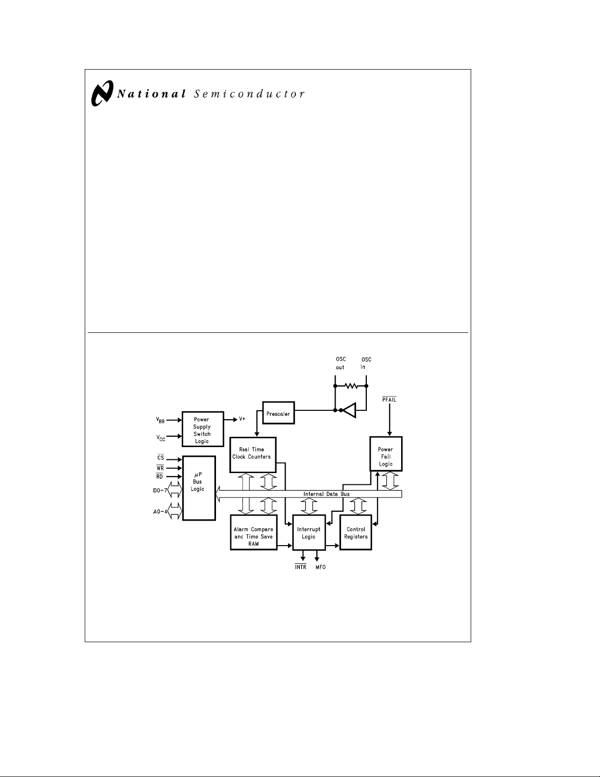
Block Diagram
l
VCC, internal circuitry will automatically switch from the
main supply to the battery supply.
The DP8573A’s interrupt structure provides three basic
types of interrupts: Periodic, Alarm/Compare, and Power
Fail. Interrupt mask and status registers enable the masking
and easy determination of each interrupt.
Features
Y
Full function real time clock/calendar
Ð 12/24 hour mode timekeeping
Ð Day of week counter
Ð Parallel resonant oscillator
Y
Power fail features
Ð Internal power supply switch to external battery
Ð Power Supply Bus glitch protection
Ð Automatic log of time into RAM at power failure
Y
On-chip interrupt structure
Ð Periodic, alarm, and power fail interrupts
l
FIGURE 1
TL/F/9981– 1
TRI-STATEÉis a registered trademark of National Semiconductor Corporation.
C
1995 National Semiconductor Corporation RRD-B30M75/Printed in U. S. A.
TL/F/9981

Absolute Maximum Ratings (Notes1&2)
If Military/Aerospace specified devices are required,
please contact the National Semiconductor Sales
Office/Distributors for availability and specifications.
Supply Voltage (V
CC
)
DC Input Voltage (VIN)
DC Output Voltage (V
OUT
)
Storage Temperature Range
Power Dissipation (PD) 500 mW
Lead Temperature (Soldering, 10 sec.) 260§C
b
0.5V toa7.0V
b
0.5V to V
b
0.5V to V
b
65§Ctoa150§C
CC
CC
a
0.5V
a
0.5V
Operation Conditions
Supply Voltage (V
) (Note 3) 4.5 5.5 V
CC
Supply Voltage (VBB) (Note 3) 2.2 V
DC Input or Output Voltage
(V
IN,VOUT
)
Operation Temperature (T
Electr-Static Discharge Rating 1 kV
Transistor Count 10,300
Typical Values
i
DIP Board 59§C/W
JA
Socket 65
iJAPLCC Board 80§C/W
Socket 88
Min Max Unit
0.0 V
b
)
A
40
CC
a
§
§
b
0.4 V
CC
85
C/W
C/W
V
C
§
DC Electrical Characteristics
V
CC
e
5Vg10%, V
BB
e
3V, V
PFAIL
l
VIH,C
e
100 pF (unless otherwise specified)
L
Symbol Parameter Conditions Min Max Units
V
IH
V
IL
V
OH
V
OL
I
IN
I
OZ
I
LKG
I
CC
I
CC
I
BB
I
BLK
Note 1:
High Level Input Voltage Any Inputs Except OSC IN, 2.0 V
(Note 4) OSC IN with External Clock V
b
0.1 V
BB
Low Level Input Voltage All Inputs Except OSC IN 0.8 V
OSC IN with External Clock 0.1 V
High Level Output Voltage I
(Excluding OSC OUT) I
Low Level Output Voltage I
(Excluding OSC OUT) I
Input Current (Except OSC IN) V
Output TRI-STATEÉCurrent V
Output High Leakage Current V
T1, MFO, INTR Pins Outputs Open Drain
Quiescent Supply Current F
(Note 6) V
Quiescent Supply Current V
(Single Supply Mode) V
(Note 7) F
Standby Mode Battery V
Supply Current OSC OUT
(Note 7) other pins
Battery Leakage 2.2VsV
eb
20 mAV
OUT
eb
4.0 mA 3.5 V
OUT
e
20 mA 0.1 V
OUT
e
4.0 mA 0.25 V
OUT
e
VCCor GND
IN
e
VCCor GND
OUT
e
VCCor GND
OUT
e
32.768 kHz
OSC
e
VCCor GND (Note 5) 250 mA
IN
e
V
VCCor GND (Note 6) 1.0 mA
IN
e
V
VIHor VIL(Note 6) 12.0 mA
IN
e
GND
BB
e
VCCor GND 40 mA
IN
e
32.768 kHz
OSC
e
GND
CC
e
open circuit,
e
GND
e
F
32.768 kHz
OSC
s
4.0V
BB
other pins at GND
e
V
GND 1.5 mA
CC
e
V
5.5V
CC
b
0.1 V
CC
g
1.0 mA
g
5.0 mA
g
5.0 mA
10 mA
b
5 mA

AC Electrical Characteristics
V
CC
e
5Vg10%, V
BB
e
3V, V
PFAIL
l
VIH,C
e
L
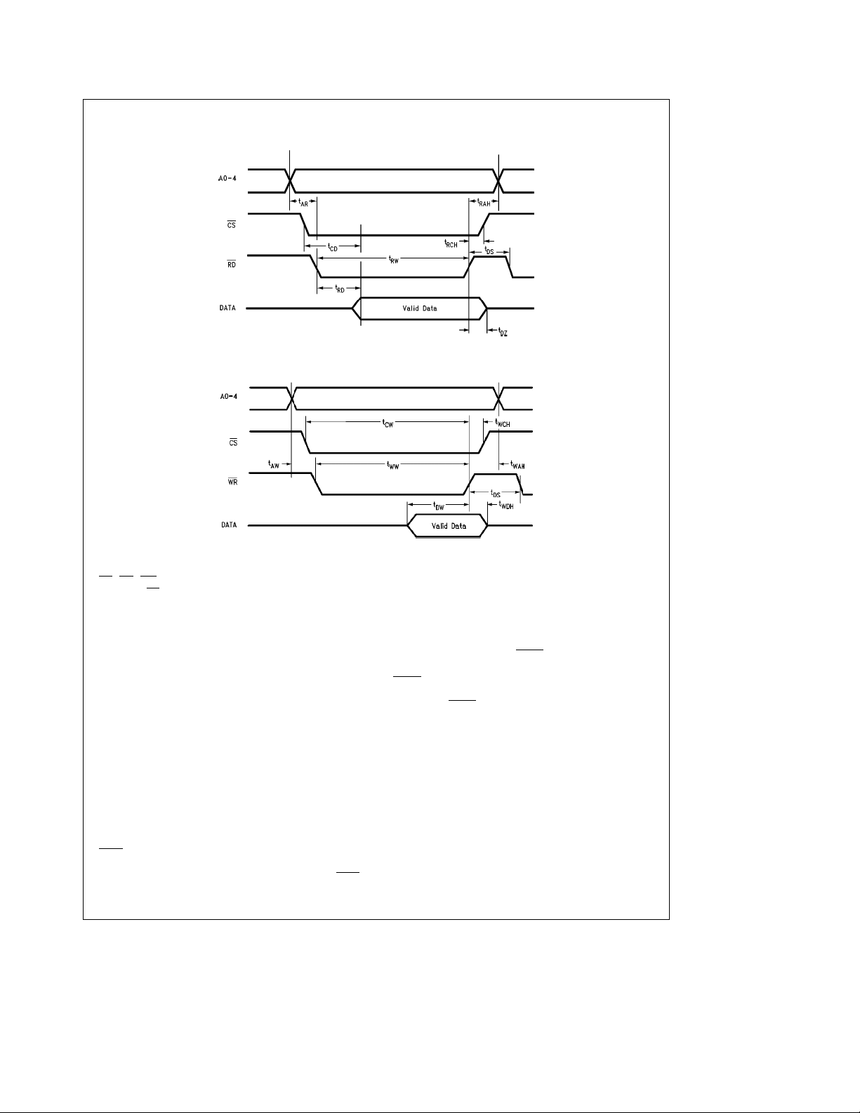
Timing Waveforms
Read Timing Diagram
TL/F/9981– 3
Write Timing Diagram
Pin Description
CS,RD,WR(Inputs): These pins interface to mP control
lines. The CS
write operations. Read and Write pins are also active low
and enable reading or writing to the RTC. All three pins are
disabled when power failure is detected. However, if a read
or write is in progress at this time, it will be allowed to complete its cycle.
A0–A4 (Inputs): These 5 pins are for register selection.
They individually control which location is to be accessed.
These inputs are disabled when power failure is detected.
OSC IN (Input): OSC OUT (Output): These two pins are
used to connect the crystal to the internal parallel resonant
oscillator. The oscillator is always running when power is
applied to V
MFO (Output): The multi-function output can be used as a
second interrupt (Power fail) output for interrupting the mP.
This pin can also provide an output for the oscillator. The
MFO output is configured as push-pull, active high for normal or single power supply operation and as an open drain
during standby mode (V
mode and a pull-up resistor is attached, it should be connected to a voltage no greater than V
INTR (Output): The interrupt output is used to interrupt the
processor when a timing event or power fail has occurred
and the respective interrupt has been enabled. The INTR
output is permanently configured active low, open drain. If in
pin is an active low enable for the read and
and VCC.
BB
l
VCC). If in battery backed
BB
.
BB
TL/F/9981– 4
battery backed mode and a pull-up resistor is attached, it
should be connected to a voltage no greater than V
output is a DC voltage level. To clear the INTR, writea1to
the appropriate bit(s) in the Main Status Register.
D0–D7 (Input/Output): These 8 bidirectional pins connect
to the host mP’s data bus and are used to read from and
write to the RTC. When the PFAIL
pin goes low and a write
is not in progress, these pins are at TRI-STATE.
PFAIL
(Input): In battery backed mode, this pin can have a
digital signal applied to it via some external power detection
logic. When PFAIL
e
logic 0 the RTC goes into a lockout
mode, in a minimum of 30 ms or a maximum of 63 ms unless
lockout delay is programmed. In the single power supply
mode, this pin is not useable as an input and should be tied
to V
. Refer to section on Power Fail Functional Descrip-
CC
tion.
V
(Battery Power Pin): This pin is connected to a back-
BB
up power supply. This power supply is switched to the internal circuitry when the V
ing this pin eliminates the need for external logic to switch in
becomes lower than VBB. Utiliz-
CC
and out the back-up power supply. If this feature is not to be
used then this pin must be tied to ground, the RTC programmed for single power supply only, and power applied to
the V
pin.
CC
: This is the main system power pin.
V
CC
GND: This is the common ground power pin for both V
and VCC.
4
BB
. The
BB
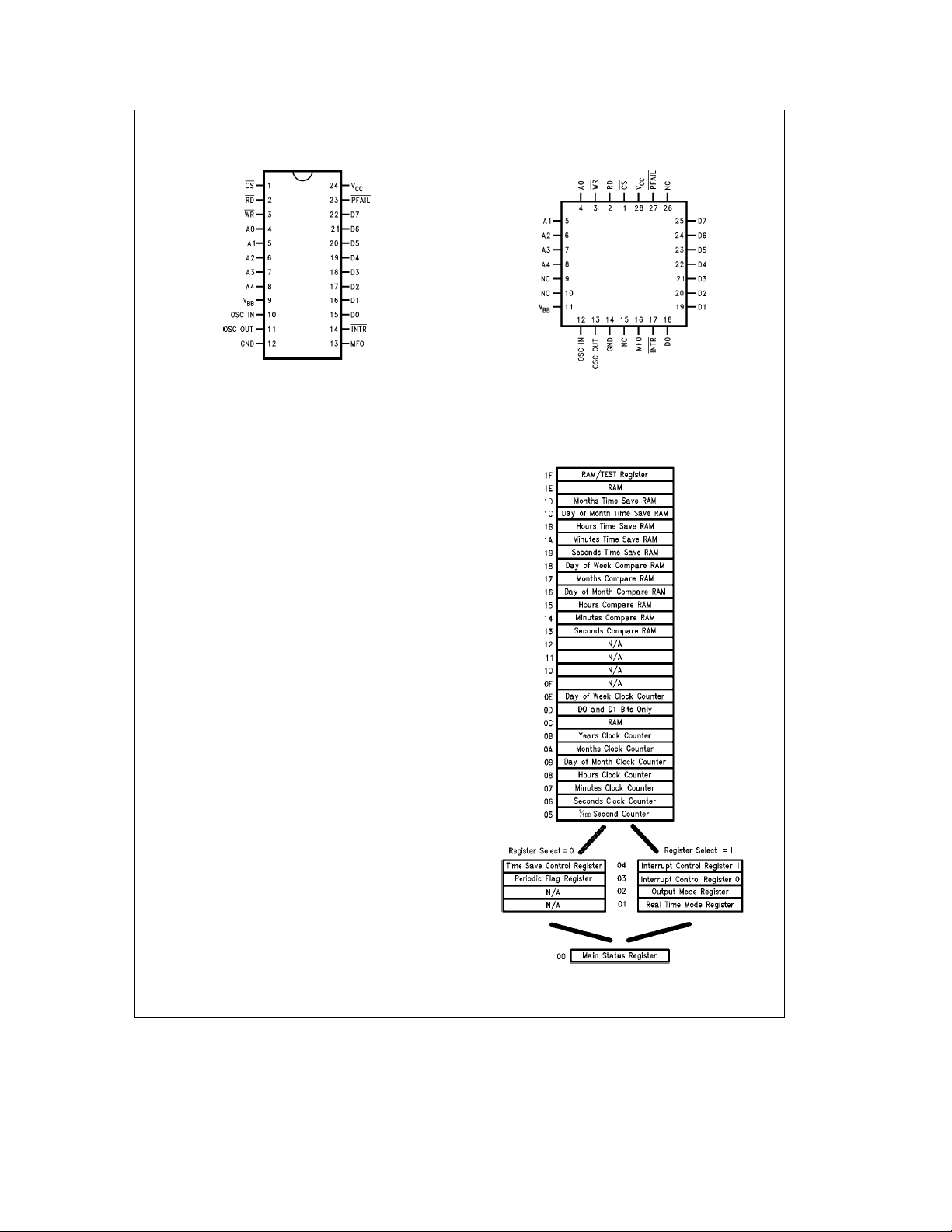
Connection Diagrams
Dual-In-Line
Plastic Chip Carrier
Top View
TL/F/9981– 5
Order Number DP8573AN
See NS Package Number N24C
Functional Description
The DP8573A contains a fast access real time clock, interrupt control logic, and power fail detect logic. All functions of
the RTC are controlled by a set of seven registers. A simplified block diagram that shows the major functional blocks is
given in
Figure 1
.
The blocks are described in the following sections:
1. Real Time Clock
2. Oscillator Prescaler
3. Interrupt Logic
4. Power Failure Logic
5. Additional Supply Management
The memory map of the RTC is shown in the memory addressing table
Register is used to select either control register block.
INITIAL POWER-ON of BOTH V
VBBand VCCmay be applied in any sequence. In order for
the power fail circuitry to function correctly, whenever power
is off, the V
maximum of 1 MX. The user should be aware that the control registers will contain random data. The user should ensure that the RTC is not in test mode (see register descriptions).
REAL TIME CLOCK FUNCTIONAL DESCRIPTION
As shown in
which count from 1/100 of a second to years. Each counter
counts in BCD and is synchronously clocked. The count sequence of the individual byte counters within the clock is
shown later in Table VII. Note that the day of week, day of
month, and month counters all roll over to 1. The hours
counter in 12 hour mode rolls over to 1 and the AM/PM bit
toggles when the hours rolls over to 12 (AM
The AM/PM bit is bit D7 in the hours counter.
All other counters roll over to 0. Upon initial application of
power the counters will contain random information.
(Figure 2).
pin must see a path to ground through a
CC
Figure 2
A control bit in the Main Status
and V
BB
CC
, the clock has 8 bytes of counters,
e
0, PMe1).
Top View
TL/F/9981– 6
Order Number DP8573AV
See NS Package Number V28A
TL/F/9981– 7
FIGURE 2. DP8573A Internal Memory Map
5
 Loading...