

APRIL 2005
CP3BT10 Reprogrammable Connectivity Processor
with Bluetooth® and USB Interfaces
1.0 General Description
The CP3BT10 connectivity processor combines high performance with the massive integration needed for embedded
Bluetooth applications. A powerful RISC core with on-chip
SRAM and Flash memory provides high computing bandwidth, communications peripherals provide high I/O bandwidth, and an external bus provides system expandability.
On-chip communications peripherals include: Bluetooth
Lower Link Controller, USB, ACCESS.bus, Microwire/SPI,
UART, and Advanced Audio Interface (AAI). Additional onchip peripherals include DMA controller, CVSD/PCM conversion module, Timing and Watchdog Unit, Versatile Timer
Unit, Multi-Function Timer, and Multi-Input Wakeup.
Bluetooth hand-held devices can be both smaller and lower
in cost for maximum consumer appeal. The low voltage and
advanced power-saving modes achieve new design points
in the trade-off between battery size and operating time for
handheld and portable applications.
In addition to providing the features needed for the next generation of embedded Bluetooth products, the CP3BT10 is
backed up by the software resources designers need for
rapid time-to-market, including an operating system, Bluetooth protocol stack implementation, reference designs, and
an integrated development environment. Combined with
National’s LMX5252 Bluetooth radio transceiver, the
CP3BT10 provides a complete Bluetooth system solution.
National Semiconductor offers a complete and industryproven application development environment for CP3BT10
applications, including the IAR Embedded Workbench,
iSYSTEM winIDEA and iC3000 Active Emulator, Bluetooth
Development Board, Bluetooth Protocol Stack, and Application Software.
CP3BT10 Reprogrammable Connectivity Processor with Bluetooth and USB Interfaces
FINAL
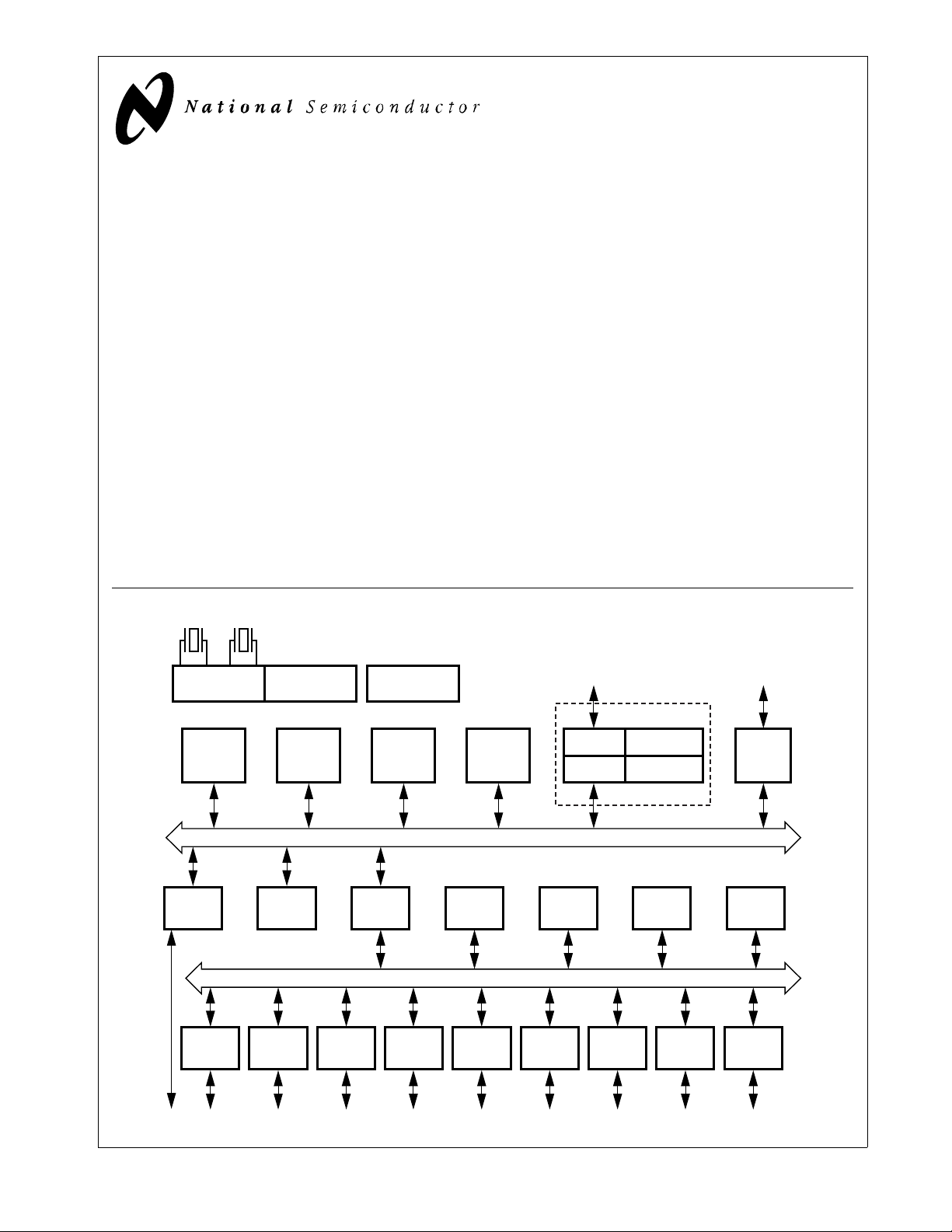
Block Diagram
12 MHz and 32 kHz
Oscillator
CR16C
CPU Core
Bus
Interface
Unit
Clock Generator
PLL and Clock
Generator
256K Bytes
Flash
Program
Memory
DMA
Controller
GPIOUSB
Audio
Interface
Power-on-Reset
8K Bytes
Flash
Peripheral
Bus
Controller
Microwire/
Data
SPI
10K Bytes
Static
RAM
CPU Core Bus
Interrupt
Control
Unit
Peripheral Bus
UART
CVSD/PCM
ACCESS
.bus
RF Interface
Protocol
Core
Versatile
Timer Unit
Bluetooth Lower
Link Controller
1K Byte
Sequencer RAM
4.5K Bytes
Data RAM
Powe r
Manage-
ment
Muti-Func-
tion Timer
Serial
Debug
Interface
Timing and
Watchdog
Unit
Multi-Input
Wake-Up
DS144
Bluetooth is a registered trademark of Bluetooth SIG, Inc. and is used under license by National Semiconductor.
TRI-STATE is a registered trademark of National Semiconductor Corporation.
©2005 National Semiconductor Corporation www.national.com

Table of Contents
1.0 General Description . . . . . . . . . . . . . . . . . . . . . . . . . . 1
CP3BT10
2.0 CPU Features . . . . . . . . . . . . . . . . . . . . . . . . . . . . . . . . 3
3.0 Device Overview . . . . . . . . . . . . . . . . . . . . . . . . . . . . . 4
3.1 CR16C CPU Core. . . . . . . . . . . . . . . . . . . . . . . . . . . . . . 4
3.2 Memory . . . . . . . . . . . . . . . . . . . . . . . . . . . . . . . . . . . . . . 4
3.3 Input/Output Ports . . . . . . . . . . . . . . . . . . . . . . . . . . . . . . 4
3.4 Bus Interface Unit . . . . . . . . . . . . . . . . . . . . . . . . . . . . . . 4
3.5 Interrupt Control Unit (ICU) . . . . . . . . . . . . . . . . . . . . . . . 4
3.6 Bluetooth LLC . . . . . . . . . . . . . . . . . . . . . . . . . . . . . . . . . 4
3.7 USB. . . . . . . . . . . . . . . . . . . . . . . . . . . . . . . . . . . . . . . . . 4
3.8 Multi-Input Wake-up . . . . . . . . . . . . . . . . . . . . . . . . . . . . 5
3.9 Triple Clock and Reset . . . . . . . . . . . . . . . . . . . . . . . . . . 5
3.10 Power Management . . . . . . . . . . . . . . . . . . . . . . . . . . . . 5
3.11 Multi-Function Timer . . . . . . . . . . . . . . . . . . . . . . . . . . . . 5
3.12 Versatile Timer Unit . . . . . . . . . . . . . . . . . . . . . . . . . . . . 5
3.13 Timing and Watchdog Module . . . . . . . . . . . . . . . . . . . . 5
3.14 UART . . . . . . . . . . . . . . . . . . . . . . . . . . . . . . . . . . . . . . . 5
3.15 Microwire/SPI . . . . . . . . . . . . . . . . . . . . . . . . . . . . . . . . . 5
3.16 ACCESS.bus Interface . . . . . . . . . . . . . . . . . . . . . . . . . . 6
3.17 DMA Controller . . . . . . . . . . . . . . . . . . . . . . . . . . . . . . . . 6
3.18 Advanced Audio interface . . . . . . . . . . . . . . . . . . . . . . . . 6
3.19 CVSD/PCM Conversion Module. . . . . . . . . . . . . . . . . . . 6
3.20 Serial Debug Interface . . . . . . . . . . . . . . . . . . . . . . . . . . 6
3.21 Development Support . . . . . . . . . . . . . . . . . . . . . . . . . . . 6
4.0 Device Pinouts. . . . . . . . . . . . . . . . . . . . . . . . . . . . . . . 7
4.1 Pin Descriptions . . . . . . . . . . . . . . . . . . . . . . . . . . . . . . 12
5.0 CPU Architecture. . . . . . . . . . . . . . . . . . . . . . . . . . . . 16
5.1 General-Purpose Registers . . . . . . . . . . . . . . . . . . . . . 16
5.2 Dedicated Address Registers . . . . . . . . . . . . . . . . . . . . 16
5.3 Processor Status Register (PSR) . . . . . . . . . . . . . . . . . 17
5.4 Configuration Register (CFG) . . . . . . . . . . . . . . . . . . . . 18
5.5 Addressing Modes . . . . . . . . . . . . . . . . . . . . . . . . . . . . 19
5.6 Stacks . . . . . . . . . . . . . . . . . . . . . . . . . . . . . . . . . . . . . . 20
5.7 Instruction Set . . . . . . . . . . . . . . . . . . . . . . . . . . . . . . . . 20
6.0 Memory. . . . . . . . . . . . . . . . . . . . . . . . . . . . . . . . . . . . 25
6.1 Operating Environment . . . . . . . . . . . . . . . . . . . . . . . . . 25
6.2 Bus Interface Unit (BIU) . . . . . . . . . . . . . . . . . . . . . . . . 26
6.3 Bus Cycles . . . . . . . . . . . . . . . . . . . . . . . . . . . . . . . . . . 26
6.4 BIU Control Registers . . . . . . . . . . . . . . . . . . . . . . . . . . 26
6.5 Wait and Hold States . . . . . . . . . . . . . . . . . . . . . . . . . . 29
7.0 System Configuration Registers . . . . . . . . . . . . . . . 30
7.1 Module Configuration Register (MCFG) . . . . . . . . . . . . 30
7.2 Module Status Register (MSTAT) . . . . . . . . . . . . . . . . . 30
8.0 Flash Memory . . . . . . . . . . . . . . . . . . . . . . . . . . . . . . 31
8.1 Flash Memory Protection . . . . . . . . . . . . . . . . . . . . . . . 31
8.2 Flash Memory Organization . . . . . . . . . . . . . . . . . . . . . 31
8.3 Flash Memory Operations. . . . . . . . . . . . . . . . . . . . . . . 32
8.4 Information Block Words . . . . . . . . . . . . . . . . . . . . . . . . 33
8.5 Flash Memory Interface Registers . . . . . . . . . . . . . . . . 35
9.0 DMA Controller . . . . . . . . . . . . . . . . . . . . . . . . . . . . . 41
9.1 Channel Assignment. . . . . . . . . . . . . . . . . . . . . . . . . . . 41
9.2 Transfer Types . . . . . . . . . . . . . . . . . . . . . . . . . . . . . . . 41
9.3 Operation Modes . . . . . . . . . . . . . . . . . . . . . . . . . . . . . 42
9.4 Software DMA Request . . . . . . . . . . . . . . . . . . . . . . . . 43
9.5 Debug Mode . . . . . . . . . . . . . . . . . . . . . . . . . . . . . . . . . 43
9.6 DMA Controller Register Set. . . . . . . . . . . . . . . . . . . . . 43
10.0 Interrupts . . . . . . . . . . . . . . . . . . . . . . . . . . . . . . . . . . 47
10.1 Non-Maskable Interrupts. . . . . . . . . . . . . . . . . . . . . . . . 47
10.2 Maskable Interrupts . . . . . . . . . . . . . . . . . . . . . . . . . . . 47
10.3 Interrupt Controller Registers . . . . . . . . . . . . . . . . . . . . 47
10.4 Maskable Interrupt Sources . . . . . . . . . . . . . . . . . . . . . 49
10.5 Nested Interrupts . . . . . . . . . . . . . . . . . . . . . . . . . . . . . 50
11.0 Triple Clock and Reset . . . . . . . . . . . . . . . . . . . . . . . 51
11.1 External Crystal Network . . . . . . . . . . . . . . . . . . . . . . . 52
11.2 Main Clock . . . . . . . . . . . . . . . . . . . . . . . . . . . . . . . . . . 52
11.3 Slow Clock . . . . . . . . . . . . . . . . . . . . . . . . . . . . . . . . . . 53
11.4 PLL Clock . . . . . . . . . . . . . . . . . . . . . . . . . . . . . . . . . . . 53
11.5 System Clock . . . . . . . . . . . . . . . . . . . . . . . . . . . . . . . . 53
11.6 Auxiliary Clocks. . . . . . . . . . . . . . . . . . . . . . . . . . . . . . . 53
11.7 Power-On Reset . . . . . . . . . . . . . . . . . . . . . . . . . . . . . . 53
11.8 External Reset . . . . . . . . . . . . . . . . . . . . . . . . . . . . . . . 53
11.9 Clock and Reset Registers . . . . . . . . . . . . . . . . . . . . . . 55
12.0 Power Management. . . . . . . . . . . . . . . . . . . . . . . . . . 57
12.1 Active Mode . . . . . . . . . . . . . . . . . . . . . . . . . . . . . . . . . 57
12.2 Power Save Mode. . . . . . . . . . . . . . . . . . . . . . . . . . . . . 57
12.3 Idle Mode . . . . . . . . . . . . . . . . . . . . . . . . . . . . . . . . . . . 57
12.4 Halt Mode . . . . . . . . . . . . . . . . . . . . . . . . . . . . . . . . . . . 57
12.5 Hardware Clock Control . . . . . . . . . . . . . . . . . . . . . . . . 57
12.6 Power Management Registers . . . . . . . . . . . . . . . . . . . 58
12.7 Switching Between Power Modes. . . . . . . . . . . . . . . . . 59
13.0 Multi-Input Wake-Up . . . . . . . . . . . . . . . . . . . . . . . . . 61
13.1 Multi-Input Wake-Up Registers . . . . . . . . . . . . . . . . . . . 61
13.2 Programming Procedures . . . . . . . . . . . . . . . . . . . . . . . 63
14.0 Input/Output Ports. . . . . . . . . . . . . . . . . . . . . . . . . . . 64
14.1 Port Registers . . . . . . . . . . . . . . . . . . . . . . . . . . . . . . . . 64
14.2 Open-Drain Operation. . . . . . . . . . . . . . . . . . . . . . . . . . 67
15.0 Bluetooth Controller . . . . . . . . . . . . . . . . . . . . . . . . . 68
15.1 RF Interface . . . . . . . . . . . . . . . . . . . . . . . . . . . . . . . . . . 68
15.2 Serial Interface . . . . . . . . . . . . . . . . . . . . . . . . . . . . . . . . 69
15.3 LMX5251 Power-Up Sequence . . . . . . . . . . . . . . . . . . . 72
15.4 LMX5252 Power-Up Sequence . . . . . . . . . . . . . . . . . . . 72
15.5 Bluetooth Sleep Mode . . . . . . . . . . . . . . . . . . . . . . . . . . 73
15.6 Bluetooth Global Registers . . . . . . . . . . . . . . . . . . . . . . 73
15.7 Bluetooth Sequencer RAM . . . . . . . . . . . . . . . . . . . . . . 73
15.8 Bluetooth Shared Data RAM . . . . . . . . . . . . . . . . . . . . . 74
16.0 USB Controller . . . . . . . . . . . . . . . . . . . . . . . . . . . . . . 75
16.1 Functional States . . . . . . . . . . . . . . . . . . . . . . . . . . . . . . 75
16.2 Endpoint Operation . . . . . . . . . . . . . . . . . . . . . . . . . . . . 75
16.3 USB Controller Registers. . . . . . . . . . . . . . . . . . . . . . . . 78
16.4 Transceiver Interface . . . . . . . . . . . . . . . . . . . . . . . . . . . 93
17.0 Advanced Audio Interface. . . . . . . . . . . . . . . . . . . . . 94
17.1 Audio Interface Signals . . . . . . . . . . . . . . . . . . . . . . . . . 94
17.2 Audio Interface Modes . . . . . . . . . . . . . . . . . . . . . . . . . . 94
17.3 Bit Clock Generation . . . . . . . . . . . . . . . . . . . . . . . . . . . 97
17.4 Frame Clock Generation . . . . . . . . . . . . . . . . . . . . . . . . 97
17.5 Audio Interface Operation . . . . . . . . . . . . . . . . . . . . . . . 97
17.6 Communication Options. . . . . . . . . . . . . . . . . . . . . . . . . 99
17.7 Audio Interface Registers. . . . . . . . . . . . . . . . . . . . . . . 102
17.8 Usage Hints . . . . . . . . . . . . . . . . . . . . . . . . . . . . . . . . . 108
18.0 CVSD/PCM Conversion Module . . . . . . . . . . . . . . . 109
18.1 Operation . . . . . . . . . . . . . . . . . . . . . . . . . . . . . . . . . . . 109
18.2 PCM Conversions . . . . . . . . . . . . . . . . . . . . . . . . . . . . 109
18.3 CVSD Conversion . . . . . . . . . . . . . . . . . . . . . . . . . . . . 110
18.4 PCM to CVSD Conversion . . . . . . . . . . . . . . . . . . . . . . 110
18.5 CVSD to PCM Conversion. . . . . . . . . . . . . . . . . . . . . . 110
18.6 Interrupt Generation. . . . . . . . . . . . . . . . . . . . . . . . . . . 110
18.7 DMA Support . . . . . . . . . . . . . . . . . . . . . . . . . . . . . . . . 110
18.8 Freeze . . . . . . . . . . . . . . . . . . . . . . . . . . . . . . . . . . . . . 111
18.9 CVSD/PCM Converter Registers . . . . . . . . . . . . . . . . . 111
19.0 UART Module . . . . . . . . . . . . . . . . . . . . . . . . . . . . . . 114
19.1 Functional Overview . . . . . . . . . . . . . . . . . . . . . . . . . . 114
19.2 UART Operation . . . . . . . . . . . . . . . . . . . . . . . . . . . . . 114
19.3 UART Registers . . . . . . . . . . . . . . . . . . . . . . . . . . . . . . 118
19.4 Baud Rate Calculations . . . . . . . . . . . . . . . . . . . . . . . . 122
20.0 Microwire/SPI Interface . . . . . . . . . . . . . . . . . . . . . . 124
20.1 Microwire Operation . . . . . . . . . . . . . . . . . . . . . . . . . . . 124
20.2 Master Mode . . . . . . . . . . . . . . . . . . . . . . . . . . . . . . . . 126
20.3 Slave Mode . . . . . . . . . . . . . . . . . . . . . . . . . . . . . . . . . 127
20.4 Interrupt Generation. . . . . . . . . . . . . . . . . . . . . . . . . . . 127
20.5 Microwire Interface Registers . . . . . . . . . . . . . . . . . . . 127
21.0 ACCESS.bus Interface. . . . . . . . . . . . . . . . . . . . . . . 130
21.1 ACB Protocol Overview . . . . . . . . . . . . . . . . . . . . . . . . 130
21.2 ACB Functional Description. . . . . . . . . . . . . . . . . . . . . 132
21.3 ACCESS.bus Interface Registers . . . . . . . . . . . . . . . . 134
21.4 Usage Hints . . . . . . . . . . . . . . . . . . . . . . . . . . . . . . . . . 138
22.0 Timing and Watchdog Module . . . . . . . . . . . . . . . . 139
22.1 TWM Structure . . . . . . . . . . . . . . . . . . . . . . . . . . . . . . . 139
22.2 Timer T0 Operation . . . . . . . . . . . . . . . . . . . . . . . . . . . 139
22.3 Watchdog Operation . . . . . . . . . . . . . . . . . . . . . . . . . . 140
22.4 TWM Registers . . . . . . . . . . . . . . . . . . . . . . . . . . . . . . 140
22.5 Watchdog Programming Procedure. . . . . . . . . . . . . . . 142
23.0 Multi-Function Timer . . . . . . . . . . . . . . . . . . . . . . . . 143
23.1 Timer Structure . . . . . . . . . . . . . . . . . . . . . . . . . . . . . . 143
23.2 Timer Operating Modes . . . . . . . . . . . . . . . . . . . . . . . . 144
23.3 Timer Interrupts . . . . . . . . . . . . . . . . . . . . . . . . . . . . . . 148
23.4 Timer I/O Functions . . . . . . . . . . . . . . . . . . . . . . . . . . . 148
23.5 Timer Registers . . . . . . . . . . . . . . . . . . . . . . . . . . . . . . 149
24.0 Versatile Timer Unit (VTU). . . . . . . . . . . . . . . . . . . . 152
24.1 VTU Functional Description . . . . . . . . . . . . . . . . . . . . . 152
24.2 VTU Registers . . . . . . . . . . . . . . . . . . . . . . . . . . . . . . . 156
25.0 Register Map. . . . . . . . . . . . . . . . . . . . . . . . . . . . . . . 160
26.0 Register Bit Fields . . . . . . . . . . . . . . . . . . . . . . . . . . 171
27.0 Electrical Characteristics . . . . . . . . . . . . . . . . . . . . 182
27.1 Absolute Maximum Ratings . . . . . . . . . . . . . . . . . . . . . 182
27.2 DC Electrical Characteristics . . . . . . . . . . . . . . . . . . . 182
27.3 USB Transceiver Electrical Characteristics . . . . . . . . 183
27.4 Flash Memory On-Chip Programming . . . . . . . . . . . . . 184
27.5 Output Signal Levels . . . . . . . . . . . . . . . . . . . . . . . . . . 185
27.6 Clock and Reset Timing . . . . . . . . . . . . . . . . . . . . . . . . 185
27.7 I/O Port Timing . . . . . . . . . . . . . . . . . . . . . . . . . . . . . . . 187
27.8 Advanced Audio Interface (AAI) Timing. . . . . . . . . . . . 188
27.9 Microwire/SPI Timing . . . . . . . . . . . . . . . . . . . . . . . . . . 190
27.10 ACCESS.bus Timing . . . . . . . . . . . . . . . . . . . . . . . . . . 195
27.11 USB Port AC Characteristics . . . . . . . . . . . . . . . . . . . . 198
27.12 Multi-Function Timer (MFT) Timing . . . . . . . . . . . . . . . 198
27.13 Versatile Timing Unit (VTU) Timing . . . . . . . . . . . . . . . 199
27.14 External Bus Timing . . . . . . . . . . . . . . . . . . . . . . . . . . . 200
28.0 Pin Assignments . . . . . . . . . . . . . . . . . . . . . . . . . . . 206
29.0 Revision History. . . . . . . . . . . . . . . . . . . . . . . . . . . . 208
30.0 Physical Dimensions . . . . . . . . . . . . . . . . . . . . . . . . 209
www.national.com 2

2.0 CPU Features
CPU Features
Fully static RISC processor core, capable of operating
from 0 to 24 MHz with zero wait/hold states
Minimum 41.7 ns instruction cycle time with a 24-MHz in-
ternal clock frequency, based on a 12-MHz external input
30 independently vectored peripheral interrupts
On-Chip Memory
256K bytes reprogrammable Flash program memory
8K bytes Flash data memory
10K bytes of static RAM data memory
Addresses up to 8 Mbytes of external memory
Broad Range of Hardware Communications Peripherals
Bluetooth Lower Link Controller (LLC) including a shared
4.5K byte Bluetooth RAM and 1K byte Bluetooth Sequencer RAM
Full-speed USB node including seven Endpoint-FIFOs
conforming to USB 1.1 specification
ACCESS.bus serial bus (compatible with Philips I
8/16-bit SPI, Microwire/Plus serial interface
Universal Asynchronous Receiver/Transmitter (UART)
Advanced Audio Interface (AAI) to connect to external 8/
13-bit PCM Codecs as well as to ISDN-Controllers
through the IOM-2 interface (slave only)
CVSD/PCM converter supporting one bidirectional audio
connection
General-Purpose Hardware Peripherals
Dual 16-bit Multi-Function Timer
Versatile Timer Unit with four subsystems (VTU)
Four channel DMA controller
Timing and Watchdog Unit
Flexible I/O
Up to 37 general-purpose I/O pins (shared with on-chip
peripheral I/O pins)
Programmable I/O pin characteristics: TRI-STATE out-
put, push-pull output, weak pull-up input, high-impedance input
Schmitt triggers on general purpose inputs
Multi-Input Wakeup
2
C bus)
CP3BT10
Extensive Power and Clock Management Support
On-chip Phase Locked Loop
Support for multiple clock options
Dual clock and reset
Power-down modes
Power Supply
I/O port operation at 2.5V to 3.3V
Core logic operation at 2.5V
On-chip power-on reset
Temperature Range
-40°C to +85°C (Industrial)
Packages
CSP-48, LQFP-100
Complete Development Environment
Pre-integrated hardware and software support for rapid
prototyping and production
Integrated environment
Project manager
Multi-file C source editor
High-level C source debugger
Comprehensive, integrated, one-stop technical support
Bluetooth Protocol Stack
Applications can interface to the high-level protocols or
directly to the low-level Host Controller Interface (HCI)
Transport layer support allows HCI command-based in-
terface over UART or USB port
Baseband (Link Controller) minimizes the performance
demand on the CPU
Link Manager (LM)
Logical Link Control and Adaptation Protocol (L2CAP)
Service Discovery Protocol (SDP)
RFCOMM Serial Port Emulation Protocol
All packet types, piconet, and scatternet functionality
supported
CP3BT10 Connectivity Processor Selection Guide
NSID
CP3BT10G38 24 -40° to +85°C 256 8 10 22 37 LQFP-100 Tray
CP3BT10G38X 24 -40° to +85°C 256 8 10 22 37 LQFP-100 1000-T&R
CP3BT10K38X 24 -40° to +85°C 256 8 10 0 21 CSP-48 2500-T&R
CP3BT10K38Y 24 -40° to +85°C 256 8 10 0 21 CSP-48 250-T&R
T&R = Tape and Reel
Speed
(MHz)
Temp. Range
Program
Flash
(kBytes)
Data
Flash
(kBytes)
SRAM
(kBytes)
External
Address
Lines
I/Os
Package
Typ e
Pack
Method
3 www.national.com

3.0 Device Overview
The CP3BT10 connectivity processor is complete microcomputer with all system timing, interrupt logic, program
CP3BT10
memory, data memory, I/O ports included on-chip, making
them well-suited to a wide range of embedded applications.
The block diagram on page 1 shows the major on-chip components of the CP3BT10.
3.1 CR16C CPU CORE
The CP3BT10 implements the CR16C CPU core module.
The high performance of the CPU core results from the implementation of a pipelined architecture with a two-bytesper-cycle pipelined system bus. As a result, the CPU can
support a peak execution rate of one instruction per clock
cycle.
For more information, please refer to the CR16C Programmer’s Reference Manual (document number 424521772101, which may be downloaded from National’s web site at
http://www.national.com).
The I/O pin characteristics are fully programmable. Each pin
can be configured to operate as a TRI-STATE output, pushpull output, weak pull-up input, or high-impedance input.
3.4 BUS INTERFACE UNIT
The Bus Interface Unit (BIU) controls access to internal/external memory and I/O. It determines the configured parameters for bus access (such as the number of wait states for
memory access) and issues the appropriate bus signals for
each requested access.
The BIU uses a set of control registers to determine how
many wait states and hold states are used when accessing
Flash program memory, and the I/O area (Port B and Port
C). At start-up, the configuration registers are set for slowest
possible memory access. To achieve fastest possible program execution, appropriate values must be programmed.
These settings vary with the clock frequency and the type of
off-chip device being accessed.
3.2 MEMORY
The CP3BT10 supports a uniform linear address space of
up to 16 megabytes. Three types of on-chip memory occupy
specific regions within this address space:
256K bytes of Flash program memory
8K bytes of Flash data memory
10K bytes of static RAM
Up to 8M bytes of external memory (100-pin devices)
The 256K bytes of Flash program memory are used to store
the application program, Bluetooth protocol stack, and realtime operating system. The Flash memory has security features to prevent unintentional programming and to prevent
unauthorized access to the program code. This memory
can be programmed with an external programming unit or
with the device installed in the application system (in-system programming).
The 8K bytes of Flash data memory are used for non-volatile storage of data entered by the end-user, such as configuration settings.
The 10K bytes of static RAM are used for temporary storage
of data and for the program stack and interrupt stack. Read
and write operations can be byte-wide or word-wide, depending on the instruction executed by the CPU.
Up to 8M bytes of external memory can be added on an external bus. The external bus is only available on devices in
100-pin packages.
For Flash program and data memory, the device internally
generates the necessary voltages for programming. No additional power supply is required.
3.3 INPUT/OUTPUT PORTS
The device has up to 37 software-configurable I/O pins, organized into five ports called Port B, Port C, Port G, Port H,
and Port I. Each pin can be configured to operate as a general-purpose input or general-purpose output. In addition,
many I/O pins can be configured to operate as inputs or outputs for on-chip peripheral modules such as the UART, timers, or Microwire/SPI interface.
3.5 INTERRUPT CONTROL UNIT (ICU)
The ICU receives interrupt requests from internal and external sources and generates interrupts to the CPU. An interrupt is an event that temporarily stops the normal flow of
program execution and causes a separate interrupt handler
to be executed. After the interrupt is serviced, CPU execution continues with the next instruction in the program following the point of interruption.
Interrupts from the timers, UART, Microwire/SPI interface,
and Multi-Input Wake-Up, are all maskable interrupts; they
can be enabled or disabled by software. There are 32
maskable interrupts, assigned to 32 linear priority levels.
The highest-priority interrupt is the Non-Maskable Interrupt
), which is generated by a signal received on the NMI
(NMI
input pin.
3.6 BLUETOOTH LLC
The integrated hardware Bluetooth Lower Link Controller
(LLC) complies to the Bluetooth Specification Version 1.1
and integrates the following functions:
4.5K-byte dedicated Bluetooth data RAM
1K-byte dedicated Bluetooth Sequencer RAM
Support of all Bluetooth 1.1 packet types
Support for fast frequency hopping of 1600 hops/s
Access code correlation and slot timing recovery circuit
Power Management Control Logic
BlueRF-compatible interface to connect with National’s
LMX5252 and other RF transceiver chips
3.7 USB
The USB node is a Universal Serial Bus (USB) Node controller compatible with USB Specification, 1.0 and 1.1. It integrates the required USB transceiver, the Serial Interface
Engine (SIE), and USB endpoint FIFOs. A total of seven
endpoint pipes are supported: one bidirectional pipe for the
mandatory control EP0 and an additional six pipes for unidirectional endpoints to support USB interrupt, bulk, and isochronous data transfers.
www.national.com 4

3.8 MULTI-INPUT WAKE-UP
The Multi-Input Wake-Up (MIWU) module can be used for
either of two purposes: to provide inputs for waking up (exiting) from the Halt, Idle, or Power Save mode; or to provide
general-purpose edge-triggered maskable interrupts from
external sources. This 16-channel module generates four
programmable interrupts to the CPU based on the signals
received on its 16 input channels. Channels can be individually enabled or disabled, and programmed to respond to
positive or negative edges.
3.9 TRIPLE CLOCK AND RESET
The Triple Clock and Reset module generates a high-speed
main System Clock from an external crystal network. It also
provides the main system reset signal and a power-on reset
function.
This module generates a slow System Clock (32.768 kHz)
from an optional external crystal network. The Slow Clock is
used for operating the device in power-save mode. The
32.768 kHz external crystal network is optional, because
the low speed System Clock can be derived from the highspeed clock by a prescaler. Also, two independent clocks divided down from the high speed clock are available on output pins.
The Triple Clock and Reset module provides the clock signals required for the operation of the various CP3BT10 onchip modules. From external crystal networks, it generates
the Main Clock, which can be scaled up to 24 MHz from an
external 12 MHz input clock, and a 32.768 kHz secondary
System Clock. The 12 MHz external clock is primarily used
as the reference frequency for the on-chip PLL. Also the
clock for modules which require a fixed clock rate (e.g. the
Bluetooth LLC and the CVSD/PCM transcoder) is generated through prescalers from the 12 MHz clock. The PLL generates the input clock for the USB node and may be used to
drive the high-speed System Clock through a prescaler. Alternatively, the high speed System Clock can be derived directly from the 12 MHz Main Clock.
In addition, this module generates the device reset by using
reset input signals coming from an external reset and various on-chip modules.
3.10 POWER MANAGEMENT
The Power Management Module (PMM) improves the efficiency of the device by changing the operating mode and
power consumption to match the required level of activity.
The device can operate in any of four power modes:
Active—The device operates at full speed using the high-
frequency clock. All device functions are fully operational.
Power Save —The device operates at reduced speed us-
ing the Slow Clock. The CPU and some modules can
continue to operate at this low speed.
Idle—The device is inactive except for the Power Man-
agement Module and Timing and Watchdog Module,
which continue to operate using the Slow Clock.
Halt—The device is inactive but still retains its internal
state (RAM and register contents).
CP3BT10
3.11 MULTI-FUNCTION TIMER
The Multi-Function Timer (MFT) module contains a pair of
16-bit timer/counter registers. Each timer/counter unit can
be configured to operate in any of the following modes:
Processor-Independent Pulse Width Modulation (PWM)
mode—Generates pulses of a specified width and duty
cycle and provides a general-purpose timer/counter.
Dual Input Capture mode—Measures the elapsed time
between occurrences of external event and provides a
general-purpose timer/counter.
Dual Independent Timer mode—Generates system tim-
ing signals or counts occurrences of external events.
Single Input Capture and Single Timer mode—Provides
one external event counter and one system timer.
3.12 VERSATILE TIMER UNIT
The Versatile Timer Unit (VTU) module contains four independent timer subsystems, each operating in either dual 8bit PWM configuration, as a single 16-bit PWM timer, or a
16-bit counter with two input capture channels. Each of the
four timer subsystems offer an 8-bit clock prescaler to accommodate a wide range of frequencies.
3.13 TIMING AND WATCHDOG MODULE
The Timing and Watchdog Module (TWM) contains a RealTime timer and a Watchdog unit. The Real-Time Clock Timing function can be used to generate periodic real-time
based system interrupts. The timer output is one of 16 inputs to the Multi-Input-Wake-Up module which can be used
to exit from a power-saving mode. The Watchdog unit is designed to detect the application program getting stuck in an
infinite loop resulting in loss of program control or “runaway”
programs. When the watchdog triggers, it resets the device.
The TWM is clocked by the low-speed System Clock.
3.14 UART
The UART supports a wide range of programmable baud
rates and data formats, parity generation, and several error
detection schemes. The baud rate is generated on-chip, under software control.
The UART offers a wake-up condition from the power-save
mode using the Multi-Input Wake-Up module.
3.15 MICROWIRE/SPI
The Microwire/SPI (MWSPI) interface module supports synchronous serial communications with other devices that
conform to Microwire or Serial Peripheral Interface (SPI)
specifications. It supports 8-bit and 16-bit data transfers.
The Microwire interface allows several devices to communicate over a single system consisting of four wires: serial in,
serial out, shift clock, and slave enable. At any given time,
the Microwire interface operates as the master or a slave.
The Microwire interface supports the full set of slave select
for multi-slave implementation.
In master mode, the shift clock is generated on chip under
software control. In slave mode, a wake-up out of powersave mode is triggered using the Multi-Input Wake-Up module.
5 www.national.com

3.16 ACCESS.BUS INTERFACE
The ACCESS.bus interface module (ACB) is a two-wire serial interface with the ACCESS.bus physical layer. It is also
compatible with Intel’s System Management Bus (SMBus)
CP3BT10
and Philips’ I
a bus master or slave, and can maintain bidirectional communications with both multiple master and slave devices.
The ACCESS.bus receiver can trigger a wake-up condition
out of the low-power modes using the Multi-Input Wake-Up
module.
2
C bus. The ACB module can be configured as
3.17 DMA CONTROLLER
The Direct Memory Access Controller (DMAC) can speed
up data transfer between memory and I/O devices or between two memories, relative to data transfers performed directly by the CPU. A method called cycle-stealing allows the
CPU and the DMAC to use the core bus in parallel. The
DMAC implements four independent DMA channels. DMA
requests from a primary and a secondary source are recognized for each DMA channel, as well as a software DMA request issued directly by the CPU. Table 1 shows the DMA
channel assignment on the CP3BT10 architecture. The following on-chip modules can assert a DMA request to the
DMAC:
CR16C (Software DMA request)
USB
UART
Advanced Audio Interface
CVSD/PCM Converter
Table 1 shows how the four DMA channels are assigned
to the modules listed above.
Table 1 DMA Channel Assignment
Channel
0
1
2
3
Primary/
Secondary
Primary USB Read/Write
Secondary UART Read
Primary UART Write
Secondary Unused N/A
Primary AAI Read
Secondary CVSD/PCM Read
Primary AAI Write
Secondary CVSD/PCM Write
Peripheral Transaction
3.18 ADVANCED AUDIO INTERFACE
The audio interface provides a serial synchronous, full-duplex interface to codecs and similar serial devices. Transmit
and receive paths operate asynchronously with respect to
each other. Each path uses three signals for communication: shift clock, frame synchronization, and data.
In case receive and transmit use separate shift clocks and
frame sync signals, the interface operates in its asynchronous mode. Alternatively, the transmit and receive path can
share the same shift clock and frame sync signals for synchronous mode operation.
The interface can handle data words of either 8- or 16-bit
length and data frames can consist of up to four slots.
In the normal mode of operation, the interface only transfers
one word at a periodic rate. In the network mode, the interface transfers multiple words at a periodic rate. The periodic
rate is also called a data frame and each word within one
frame is called a slot. The beginning of each new data frame
is marked by the frame sync signal.
3.19 CVSD/PCM CONVERSION MODULE
The CVSD/PCM module performs conversion between
CVSD and PCM data, in which the CVSD encoding is as defined in the Bluetooth specification 1.0 and the PCM data
can be 8-bit µ-Law, 8-bit A-Law, or 13-bit to 16-bit Linear.
3.20 SERIAL DEBUG INTERFACE
The Serial Debug Interface module (SDI module) provides
a JTAG-based serial link to an external debugger, for example running on a PC. In addition, the SDI module integrates
an on-chip debug module, which allows the user to set up to
four hardware breakpoints on instruction execution and data
transfer. The SDI module can act as a CPU bus master to
access all memory mapped resources, such as RAM and
peripherals. It also provides fast program download into the
on-chip Flash program memory using the JTAG interface.
Note: The SDI module may assert Freeze mode to gather
information, which may cause periodic fluctuations in response (bus availability, interrupt latency, etc.). Anomalous
behavior often may be traced to SDI activity.
3.21 DEVELOPMENT SUPPORT
In addition to providing the features needed for the next generation of embedded Bluetooth products, the CP3BT10 is
backed up by the software resources designers need for
rapid time-to-market, including an operating system, Bluetooth protocol stack implementation, peripheral drivers, reference designs, and an integrated development
environment. Combined with National’s LMX5252 Bluetooth
radio transceiver, the CP3BT10 provides a total Bluetooth
system solution.
National Semiconductor offers a complete and industryproven application development environment for CP3BT10
applications, including the IAR Embedded Workbench,
iSYSTEM winIDEA and iC3000 Active Emulator, Bluetooth
Development Board, Bluetooth Protocol Stack, and Application Software. See your National Semiconductor sales representative for current information on availability and
features of emulation equipment and evaluation boards.
www.national.com 6
4.0 Device Pinouts
CP3BT10
2 MHz Crystal
or Ext. Clock
32.768 kHz
Crystal
Powe r
Supply
Chip Reset
JTAG I/F to
Debugger/
Programmer
ACCESS.bus
USB
Mode
Selection
2
4
6
X1CKI/BBCLK
X1CKO
X2CKI
X2CKO
AVCC
AGND
CP3BT10
VCC
(LQFP-100)
IOVCC
GND
RESET
TMS
TDI
TDO
TCK
RDY
SDA
SCL
+
D
D-
UVCC
UGND
ENV0
ENV1
ENV2
PB[7:0]
PC[7:0]
A[21:0]
SEL0
SEL1
SEL2
SELIO
WR0
WR1
RD
RFDATA
PIO/RFSYNC
PI1/RFCE
PI3/SCLK
PI4/SDAT
PI5/SLE
PI6/BTSEQ2/WUI9
PI7/BTSEQ3/TA
PG0/RXD/WUI10
PG1/TXD/WUI11
PG2/RTS/WUI12
PG3/CTS/WUI13
PH0/MSK/TIO1
PH1/MDIDO/TIO2
PH2/MDODI/TIO3
PH3/MWCS/TIO4
PH4/SCK/TIO5
PH5/SFS/TIO6
PH6/STD/TIO7
PH7/SRD/TIO8
PG5/SRFS/NMI
PI2/BTSEQ3/SRCLK
8
8
22
12 MHz Crystal
External
Bus
Interface
RF Interface
RF/MIWU
RF/MFT
UART/
MIWU
Microwire/
SPI/
VTU
AAI/
VTU
AAI/NMI
RF/AAI
or Ext. Clock
32.768 kHz
Crystal/
Powe r
Supply
Chip Reset
JTAG I/F to
Debugger/
Programmer
Mode
Selection
2
2
4
X1CKI/BBCLK
X1CKO
X2CKI
X2CKO
AVCC
AGND
CP3BT10
VCC
(CSP-48)
IOVCC
GND
RESET
TMS
TDI
TDO
TCK
RDY
ENV0
ENV1
D
UVCC
UGND
RFDATA
PIO/RFSYNC
PI1/RFCE
PI3/SCLK
PI4/SDAT
PI5/SLE
PI6/BTSEQ2/WUI9
PI7/BTSEQ3/TA
PG0/RXD/WUI10
PG1/TXD/WUI11
PG2/RTS/WUI12
PG3/CTS/WUI13
PH0/MSK/TIO1
PH1/MDIDO/TIO2
PH2/MDODI/TIO3
PH3/MWCS/TIO4
PH4/SCK/TIO5
PH5/SFS/TIO6
PH6/STD/TIO7
PH7/SRD/TIO8
PG5/SRFS/NMI
PI2/BTSEQ1/SRCLK
+
D-
USB
RF Interface
RF/MIWU
RF/MFT
UART/
MIWU
Microwire/
SPI/
VTU
AAI/
VTU
AAI/NMI
RF/AAI
DS148
Table 2 Pin Assignments for 100-Pin Package
Pin Name Alternate Function(s) Pin Numbers Type
A14 1 O
A13 2 O
A12 3 O
A11 4 O
A10 5 O
PH6 STD/TIO7 6 GPIO
PH7 SRD/TIO8 7 GPIO
ENV1 8 I/O
A9 9 O
A8 10 O
A7 11 O
A6 12 O
A5 13 O
7 www.national.com

CP3BT10
Table 2 Pin Assignments for 100-Pin Package
Pin Name Alternate Function(s) Pin Numbers Type
A4 14 O
VCC 15 PWR
X2CKI 16 I
X2CKO 17 O
GND 18 PWR
AVC C 19 PWR
AGND 20 PWR
IOVCC 21 PWR
X1CKO 22 O
X1CKI BBCLK 23 I
GND 24 PWR
RFDATA 25 I/O
A3 26 O
A2 27 O
A1 28 O
A0 29 O
PI0 RFSYNC 30 GPIO
PI1 RFCE 31 GPIO
PI2 BTSEQ1/SRCLK 32 GPIO
PB0 D0 33 GPIO
PB1 D1 34 GPIO
PB2 D2 35 GPIO
PB3 D3 36 GPIO
PB4 D4 37 GPIO
PB5 D5 38 GPIO
PB6 D6 39 GPIO
PB7 D7 40 GPIO
GND 41 PWR
IOVCC 42 PWR
PI3 SCLK 43 GPIO
PI4 SDAT 44 GPIO
PI5 SLE
PI6 BTSEQ2/WUI9 46 GPIO
PI7 BTSEQ3/TA 47 GPIO
PG0 RXD/WUI10 48 GPIO
PG1 TXD/WUI11 49 GPIO
PC0 D8 50 GPIO
PG2 RTS
PG3 CTS
PC1 D9 53 GPIO
PC2 D10 54 GPIO
PC3 D11 55 GPIO
PC4 D12 56 GPIO
/WUI12 51 GPIO
/WUI13 52 GPIO
45 GPIO
www.national.com 8

Table 2 Pin Assignments for 100-Pin Package
Pin Name Alternate Function(s) Pin Numbers Type
PC5 D13 57 GPIO
PC6 D14 58 GPIO
PC7 D15 59 GPIO
PG5 SRFS/NMI
TMS 61 I
TCK 62 I
TDI 63 I
GND 64 PWR
IOVCC 65 PWR
ENV2 66 I/O
SEL0 67 O
SCL 68 I/O
SDA 69 I/O
TDO 70 O
D- 71 I/O
D+ 72 I/O
UVCC 73 PWR
UGND 74 PWR
RDY 75 O
SEL1 76 O
SEL2 77 O
SELIO 78 O
A21 79 O
A20 80 O
PH0 MSK/TIO1 81 GPIO
PH1 MDIDO/TIO2 82 GPIO
PH2 MDODI/TIO3 83 GPIO
PH3 MWCS
ENV0 85 I/O
IOVCC 86 PWR
GND 87 PWR
VCC 88 PWR
GND 89 PWR
RESET 90 I
RD 91 O
WR0 92 O
WR1 93 O
A19 94 O
A18 95 O
A17 96 O
A16 97 O
A15 98 O
/TIO4 84 GPIO
60 GPIO
CP3BT10
9 www.national.com

Table 2 Pin Assignments for 100-Pin Package
Pin Name Alternate Function(s) Pin Numbers Type
CP3BT10
PH4 SCK/TIO5 99 GPIO
PH5 SFS/TIO6 100 GPIO
Note 1: The ENV0, ENV1, ENV2, TCK, TDI, and TMS pins each have a weak pull-up to keep the input from floating.
Note 2: The RESET
Note 3: These functions are always enabled, due to the direct low-impedance path to these pins.
input has a weak pulldown.
Table 3 Pin Assignments for 48-Pin Package
Pin Name Alternate Function(s) Pin Number Type
PH6 STD/TIO7
PH7 SRD/TIO8
ENV1
VCC
X2CKI
X2CKO
GND
AVC C
AGND
IOVCC
X1CKO
X1CKI BBCLK
GND
RFDATA
PI0 RFSYNC
PI1 RFCE
PI2 BTSEQ1/SRCLK
PI3 SCLK
PI4 SDAT
PI5 SLE
PI6 BTSEQ2/WUI9
PI7 BTSEQ3/TA
PG0 RXD/WUI10
PG1 TXD/WUI11
PG2 RTS
PG3 CTS
/WUI12
/WUI13
PG5 SRFS/NMI
TMS
TCK
TDI
GND
IOVCC
TDO
D-
D+
UVCC
10
11
12
13
14
15
16
17
18
19
20
21
22
23
24
25
26
27
28
29
30
31
32
33
34
35
36
1
2
3
4
5
6
7
8
9
GPIO
GPIO
I/O
PWR
I
O
PWR
PWR
PWR
PWR
O
I
PWR
I/O
GPIO
GPIO
GPIO
GPIO
GPIO
GPIO
GPIO
GPIO
GPIO
GPIO
GPIO
GPIO
GPIO
I
I
I
PWR
PWR
O, GPIO
O, GPIO
I/O
PWR, I/O
www.national.com 10

Pin Name Alternate Function(s) Pin Number Type
UGND
RDY
PH0 MSK/TIO1
PH1 MDIDO/TIO2
PH2 MDODI/TIO3
PH3 MWCS
/TIO4
ENV0
VCC
GND
RESET
PH4 SCK/TIO5
PH5 SFS/TIO6
Note 1: The ENV0, ENV1 and ENV2, TCK, TDI and TMS pins each have a weak pull-up to keep the input from floating.
Note 2: The RESET
Note 3: These functions are always enabled, due to the direct low-impedance path to these pins.
input has a weak pulldown.
37
38
39
40
41
42
43
44
45
46
47
48
CP3BT10
PWR, O
O
GPIO
GPIO
GPIO
GPIO
I/O
PWR
PWR
I
GPIO
GPIO
11 www.national.com

4.1 PIN DESCRIPTIONS
Some pins may be enabled as general-purpose I/O-port
pins or as alternate functions associated with specific peripherals or interfaces. These pins may be individually con-
CP3BT10
Table 4 CP3BT10 Pin Descriptions for the 100-Pin LQFP Package
figured as port pins, even when the associated peripheral or
interface is enabled. Table 4 lists the device pins.
Name Pins I/O Primary Function
X1CKI 1 Input 12 MHz Oscillator Input BBCLK BB reference clock for the RF Interface
X1CKO 1 Output 12 MHz Oscillator Output None None
X2CKI 1 Input 32 kHz Oscillator Input None None
X2CKO 1 Output 32 kHz Oscillator Output None None
AVCC 1 Input PLL Analog Power Supply None None
IOVCC 4 Input 2.5V - 3.3V I/O Power Supply None None
VCC 2 Input
GND 6 Input Reference Ground None None
AGND 1 Input PLL Analog Ground None None
RESET
TMS 1 Input
TDI 1 Input
TDO 1 Output JTAG Test Data Output None None
TCK 1 Input
RDY
1 Input Chip general reset None None
1 Output NEXUS Ready Output None None
2.5V Core Logic
Power Supply
JTAG Test Mode Select
(with internal weak pull-up)
JTAG Test Data Input
(with internal weak pull-up)
JTAG Test Clock Input
(with internal weak pull-up)
Alternate
Name
None None
None None
None None
None None
Alternate Function
PG0 1 I/O Generic I/O
PG1 1 I/O Generic I/O
PG2 1 I/O Generic I/O
PG3 1 I/O Generic I/O
PG5 1 I/O Generic I/O
PH0 1 I/O Generic I/O
PH1 1 I/O Generic I/O
PH2 1 I/O Generic I/O
RXD UART Receive Data Input
WUI10 Multi-Input Wake-Up Channel 10
TXD UART Transmit Data Output
WUI11 Multi-Input Wake-Up Channel 11
RTS
WUI12 Multi-Input Wake-Up Channel 12
CTS UART Clear-To-Send Input
WUI13 Multi-Input Wake-Up Channel 13
SRFS AAI Receive Frame Sync
NMI
MSK SPI Shift Clock
TIO1 Versatile Timer Channel 1
MDIDO SPI Master In Slave Out
TIO2 Versatile Timer Channel 2
MDODI SPI Master Out Slave In
TIO3 Versatile Timer Channel 3
UART Ready-To-Send Output
Non-Maskable Interrupt Input
www.national.com 12

CP3BT10
Name Pins I/O Primary Function
PH3 1 I/O Generic I/O
PH4 1 I/O Generic I/O
PH5 1 I/O Generic I/O
PH6 1 I/O Generic I/O
PH7 1 I/O Generic I/O
RFDATA 1 I/O Bluetooth RX/TX Data Pin None None
PI0 1 I/O Generic I/O RFSYNC BT AC Correlation/TX Enable Output
PI1 1 I/O Generic I/O RFCE BT RF Chip Enable Output
PI2 1 I/O Generic I/O
PI3 1 I/O Generic I/O SCLK BT Serial I/F Shift Clock Output
Alternate
Name
MWCS
TIO4 Versatile Timer Channel 4
SCK AAI Clock
TIO5 Versatile Timer Channel 5
SFS AAI Frame Synchronization
TIO6 Versatile Timer Channel 6
STD AAI Transmit Data Output
TIO7 Versatile Timer Channel 7
SRD AAI Receive Data Input
TIO8 Versatile Timer Channel 8
BTSEQ1 Bluetooth Sequencer Status
SRCLK AAI Receive Clock
SPI Slave Select Input
Alternate Function
PI4 1 I/O Generic I/O SDAT BT Serial I/F Data
PI5 1 I/O Generic I/O SLE
PI6 1 I/O Generic I/O
PI7 1 I/O Generic I/O
SDA 1 I/O ACCESS.bus Serial Data None None
SCL 1 I/O ACCESS.bus Clock None None
D+ 1 I/O USB D+ Upstream Port None None
D- 1 I/O USB D- Upstream Port None None
UVCC 1 Input 3.3V USB Transceiver Supply None None
UGND 1 Input USB Transceiver Ground None None
PB[7:0] 8 I/O Generic I/O D[7:0] External Data Bus Bit 0 to 7
PC[7:0] 8 I/O Generic I/O D[15:8] External Data Bus Bit 8 to 15
A[21:0] 22 Output
SEL0
SEL1
SEL2
SELIO
1 Output Chip Select for Zone 0 None None
1 Output Chip Select for Zone 1 None None
1 Output Chip Select for Zone 2 None None
1 Output Chip Select for Zone I/O Zone None None
External Address Bus
Bit 0 to 21
WUI9 Multi-Input Wake-Up Channel 9
BTSEQ2 Bluetooth Sequencer Status
TA Multi Function Timer Port A
BTSEQ3 Bluetooth Sequencer Status
None None
BT Serial I/F Load Enable Output
WR0
WR1
1 Output External Memory Write Low Byte None None
1 Output External Memory Write High Byte None None
13 www.national.com

Name Pins I/O Primary Function
Alternate
Name
Alternate Function
RD
CP3BT10
ENV0 1 I/O
ENV1 1 I/O
ENV2 1 I/O
Name Pins I/O Primary Function
X1CKI 1 Input 12 MHz Oscillator Input BBCLK BB reference clock for the RF Interface
X1CKO 1 Output 12 MHz Oscillator Output None None
X2CKI 1 Input 32 kHz Oscillator Input None None
X2CKO 1 Output 32 kHz Oscillator Output None None
AVCC 1 Input PLL Analog Power Supply None None
IOVCC 2 Input 2.5V - 3.3V I/O Power Supply None None
VCC 2 Input
GND 4 Input Reference Ground None None
1 Output External Memory Read None None
Special mode select input with internal pull-up during reset
Special mode select input with internal pull-up during reset
Special mode select input with internal pull-up during reset
Table 5 CP3BT10 Pin Descriptions for the 48-Pin CSP
2.5V Core Logic
Power Supply
PLLCLK PLL Clock Output
CPUCLK CPU Clock Output
SLOWCLK Slow Clock Output
Alternate
Name
None None
Alternate Function
AGND 1 Input PLL Analog Ground None None
RESET
TMS 1 Input
TDI 1 Input
TDO 1 Output JTAG Test Data Output None None
TCK 1 Input
RDY
PG0 1 I/O Generic I/O
PG1 1 I/O Generic I/O
PG2 1 I/O Generic I/O
PG3 1 I/O Generic I/O
PG5 1 I/O Generic I/O
1 Input Chip general reset None None
JTAG Test Mode Select
(with internal weak pull-up)
JTAG Test Data Input
(with internal weak pull-up)
JTAG Test Clock Input
(with internal weak pull-up)
1 Output NEXUS Ready Output None None
None None
None None
None None
RXD UART Receive Data Input
WUI10 Multi-Input Wake-Up Channel 10
TXD UART Transmit Data Output
WUI11 Multi-Input Wake-Up Channel 11
RTS
WUI12 Multi-Input Wake-Up Channel 12
CTS
WUI13 Multi-Input Wake-Up Channel 13
SRFS AAI Receive Frame Sync
NMI
UART Ready-To-Send Output
UART Clear-To-Send Input
Non-Maskable Interrupt Input
www.national.com 14

CP3BT10
Name Pins I/O Primary Function
PH0 1 I/O Generic I/O
PH1 1 I/O Generic I/O
PH2 1 I/O Generic I/O
PH3 1 I/O Generic I/O
PH4 1 I/O Generic I/O
PH5 1 I/O Generic I/O
PH6 1 I/O Generic I/O
PH7 1 I/O Generic I/O
Alternate
Name
MSK SPI Shift Clock
TIO1 Versatile Timer Channel 1
MDIDO SPI Master In Slave Out
TIO2 Versatile Timer Channel 2
MDODI SPI Master Out Slave In
TIO3 Versatile Timer Channel 3
MWCS
TIO4 Versatile Timer Channel 4
SCK AAI Clock
TIO5 Versatile Timer Channel 5
SFS AAI Frame Synchronization
TIO6 Versatile Timer Channel 6
STD AAI Transmit Data Output
TIO7 Versatile Timer Channel 7
SRD AAI Receive Data Input
TIO8 Versatile Timer Channel 8
SPI Slave Select Input
Alternate Function
RFDATA 1 I/O Bluetooth RX/TX Data Pin None None
PI0 1 I/O Generic I/O RFSYNC BT AC Correlation/TX Enable Output
PI1 1 I/O Generic I/O RFCE BT RF Chip Enable Output
PI2 1 I/O Generic I/O
PI3 1 I/O Generic I/O SCLK BT Serial I/F Shift Clock Output
PI4 1 I/O Generic I/O SDAT BT Serial I/F Data
PI5 1 I/O Generic I/O SLE
PI6 1 I/O Generic I/O
PI7 1 I/O Generic I/O
D+ 1 I/O USB D+ Upstream Port None None
D- 1 I/O USB D- Upstream Port None None
UVCC 1 Input 3.3V USB Transceiver Supply None None
UGND 1 Input USB Transceiver Ground None None
ENV0 1 I/O
ENV1 1 I/O
Special mode select input with internal pull-up during reset
Special mode select input with internal pull-up during reset
BTSEQ1 Bluetooth Sequencer Status
SRCLK AAI Receive Clock
BT Serial I/F Load Enable Output
WUI9 Multi-Input Wake-Up Channel 9
BTSEQ2 Bluetooth Sequencer Status
TA Multi Function Timer Port A
BTSEQ3 Bluetooth Sequencer Status
PLLCLK PLL Clock Output
CPUCLK CPU Clock Output
15 www.national.com

5.0 CPU Architecture
The CP3BT10 uses the CR16C third-generation 16-bit
CompactRISC processor core. The CPU implements a Re-
CP3BT10
duced Instruction Set Computer (RISC) architecture that allows an effective execution rate of up to one instruction per
clock cycle. For a detailed description of the CPU16C architecture, see the CompactRISC CR16C Programmer’s Ref-
erence Manual which is available on the National
Semiconductor web site (http://www.nsc.com).
The CR16C CPU core includes these internal registers:
General-purpose registers (R0-R13, RA, and SP)
Dedicated address registers (PC, ISP, USP, and INT-
BASE)
Processor Status Register (PSR)
Configuration Register (CFG)
The R0-R11, PSR, and CFG registers are 16 bits wide. The
R12, R13, RA, SP, ISP and USP registers are 32 bits wide.
The PC register is 24 bits wide. Figure 1 shows the CPU
registers.
Dedicated Address Registers
31
ISPH
USPH
INTBASEH
15
23
PC
ISPL
USPL
INTBASEL
Processor Status Register
15
PSR
Configuration Register
15
CFG
0
0
0
31
Figure 1. CPU Registers
Some register bits are designated as “reserved.” Software
must write a zero to these bit locations when it writes to the
register. Read operations from reserved bit locations return
undefined values.
5.1 GENERAL-PURPOSE REGISTERS
The CompactRISC CPU features 16 general-purpose registers. These registers are used individually as 16-bit operands or as register pairs for operations on addresses
greater than 16 bits.
General-purpose registers are defined as R0 through
R13, RA, and SP.
Registers are grouped into pairs based on the setting of
the Short Register bit in the Configuration Register
(CFG.SR). When the CFG.SR bit is set, the grouping of
register pairs is upward-compatible with the architecture
of the earlier CR16A/B CPU cores: (R1,R0), (R2,R1) ...
(R11,R10), (R12_L, R11), (R13_L, R12_L), (R14_L,
R13_L) and SP. (R14_L, R13_L) is the same as
(RA,ERA).
General-Purpose Registers
15 0
R0
R1
R2
R3
R4
R5
R6
R7
R8
R9
R10
R11
R12
R13
RA
SP
DS004
When the CFG.SR bit is clear, register pairs are grouped
in the manner used by native CR16C software: (R1,R0),
(R2,R1) ... (R11,R10), (R12_L, R11), R12, R13, RA, SP.
R12, R13, RA, and SP are 32-bit registers for holding addresses greater than 16 bits.
With the recommended calling convention for the architecture, some of these registers are assigned special hardware
and software functions. Registers R0 to R13 are for generalpurpose use, such as holding variables, addresses, or index
values. The SP register holds a pointer to the program runtime stack. The RA register holds a subroutine return address. The R12 and R13 registers are available to hold base
addresses used in the index addressing mode.
If a general-purpose register is specified by an operation
that is 8 bits long, only the lower byte of the register is used;
the upper part is not referenced or modified. Similarly, for
word operations on register pairs, only the lower word is
used. The upper word is not referenced or modified.
5.2 DEDICATED ADDRESS REGISTERS
The CR16C has four dedicated address registers to implement specific functions: the PC, ISP, USP, and INTBASE
registers.
5.2.1 Program Counter (PC) Register
The 24-bit value in the PC register points to the first byte of
the instruction currently being executed. CR16C instructions are aligned to even addresses, therefore the least significant bit of the PC is always 0. At reset, the PC is
initialized to 0 or an optional predetermined value. When a
warm reset occurs, value of the PC prior to reset is saved in
the (R1,R0) general-purpose register pair.
5.2.2 Interrupt Stack Pointer (ISP)
The 32-bit ISP register points to the top of the interrupt
stack. This stack is used by hardware to service exceptions
(interrupts and traps). The stack pointer may be accessed
as the ISP register for initialization. The interrupt stack can
be located anywhere in the CPU address space. The ISP
cannot be used for any purpose other than the interrupt
stack, which is used for automatic storage of the CPU registers when an exception occurs and restoration of these
registers when the exception handler returns. The interrupt
stack grows downward in memory. The least significant bit
and the 8 most significant bits of the ISP register are always
0.
5.2.3 User Stack Pointer (USP)
The USP register points to the top of the user-mode program stack. Separate stacks are available for user and supervisor modes, to support protection mechanisms for
multitasking software. The processor mode is controlled by
the U bit in the PSR register (which is called PSR.U in the
shorthand convention). Stack grow downward in memory. If
the USP register points to an illegal address (any address
greater than 0x00FF_FFFF) and the USP is used for stack
access, an IAD trap is taken.
www.national.com 16

5.2.4 Interrupt Base Register (INTBASE)
The INTBASE register holds the address of the dispatch table for exceptions. The dispatch table can be located anywhere in the CPU address space. When loading the
INTBASE register, bits 31 to 24 and bit 0 must written with 0.
5.3 PROCESSOR STATUS REGISTER (PSR)
The PSR provides state information and controls operating
modes for the CPU. The format of the PSR is shown below.
15 12 11 10 9 8 7 6 5 4 3 2 1 0
Reserved I P E 0 N Z F 0 U L T C
C The Carry bit indicates whether a carry or bor-
row occurred after addition or subtraction.
0 – No carry or borrow occurred.
1 – Carry or borrow occurred.
T The Trace bit enables execution tracing, in
which a Trace trap (TRC) is taken after every
instruction. Tracing is automatically disabled
during the execution of an exception handler.
– Tracing disabled.
0
1 – Tracing enabled.
L The Low bit indicates the result of the last
comparison operation, with the operands interpreted as unsigned integers.
– Second operand greater than or equal to
0
first operand.
1 – Second operand less than first operand.
U The User Mode bit controls whether the CPU
is in user or supervisor mode. In supervisor
mode, the SP register is used for stack operations. In user mode, the USP register is used
instead. User mode is entered by executing
the Jump USR instruction. When an exception
is taken, the exception handler automatically
begins execution in supervisor mode. The
USP register is accessible using the Load
Processor Register (LPR/LPRD) instruction in
supervisor mode. In user mode, an attempt to
access the USP register generates a UND
trap.
– CPU is executing in supervisor mode.
0
– CPU is executing in user mode.
1
F The Flag bit is a general condition flag for sig-
nalling exception conditions or distinguishing
the results of an instruction, among other
thing uses. For example, integer arithmetic instructions use the F bit to indicate an overflow
condition after an addition or subtraction operation.
Z The Zero bit is used by comparison opera-
tions. In a comparison of integers, the Z bit is
set if the two operands are equal. If the operands are unequal, the Z bit is cleared.
– Source and destination operands un-
0
equal.
1 – Source and destination operands equal.
N The Negative bit indicates the result of the last
comparison operation, with the operands interpreted as signed integers.
– Second operand greater than or equal to
0
first operand.
1 – Second operand less than first operand.
E The Local Maskable Interrupt Enable bit en-
ables or disables maskable interrupts. If this
bit and the Global Maskable Interrupt Enable
(I) bit are both set, all interrupts are enabled.
If either of these bits is clear, only the nonmaskable interrupt is enabled. The E bit is set
by the Enable Interrupts (EI) instruction and
cleared by the Disable Interrupts (DI) instruction.
– Maskable interrupts disabled.
0
1 – Maskable interrupts enabled.
P The Trace Trap Pending bit is used together
with the Trace (T) bit to prevent a Trace (TRC)
trap from occurring more than once for one instruction. At the beginning of the execution of
an instruction, the state of the T bit is copied
into the P bit. If the P bit remains set at the end
of the instruction execution, the TRC trap is
taken.
– No trace trap pending.
0
– Trace trap pending.
1
I The Global Maskable Interrupt Enable bit is
used to enable or disable maskable interrupts.
If this bit and the Local Maskable Interrupt Enable (E) bit are both set, all maskable interrupts are taken. If either bit is clear, only the
non-maskable interrupt is taken. Unlike the E
bit, the I bit is automatically cleared when an
interrupt occurs and automatically set upon
completion of an interrupt handler.
– Maskable interrupts disabled.
0
1 – Maskable interrupts enabled.
Bits Z, C, L, N, and F of the PSR are referenced from assembly language by the condition code in conditional
branch instructions. A conditional branch instruction may
cause a branch in program execution, based on the value of
one or more of these PSR bits. For example, one of the
Bcond instructions, BEQ (Branch EQual), causes a branch
if the PSR.Z bit is set.
On reset, bits 0 through 11 of the PSR are cleared, except
for the PSR.E bit, which is set. On warm reset, the values of
each bit before reset are copied into the R2 general-purpose register. Bits 4 and 8 of the PSR have a constant value
of 0. Bits 12 through 15 are reserved. In general, status bits
are modified only by specific instructions. Otherwise, status
bits maintain their values throughout instructions which do
not implicitly affect them.
CP3BT10
17 www.national.com

5.4 CONFIGURATION REGISTER (CFG)
The CFG register is used to enable or disable various operating modes and to control optional on-chip caches. Because the CP3BT10 does not have cache memory, the
CP3BT10
cache control bits in the CFG register are reserved. All CFG
bits are cleared on reset.
15 10 9 8 7 6 5 2 1 0
Reserved SR ED 0 0 Reserved 0 0
ED The Extended Dispatch bit selects whether
the size of an entry in the interrupt dispatch table (IDT) is 16 or 32 bits. Each entry holds the
address of the appropriate exception handler.
When the IDT has 16-bit entries, and all exception handlers must reside in the first 128K
of the address space. The location of the IDT
is held in the INTBASE register, which is not
affected by the state of the ED bit.
– Interrupt dispatch table has 16-bit entries.
0
1 – Interrupt dispatch table has 32-bit entries.
SR The Short Register bit enables a compatibility
mode for the CR16B large model. In the
CR16C core, registers R12, R13, and RA are
extended to 32 bits. In the CR16B large model, only the lower 16 bits of these registers are
used, and these “short registers” are paired
together for 32-bit operations. In this mode,
the (RA, R13) register pair is used as the extended RA register, and address displacements relative to a single register are
supported with offsets of 0 and 14 bits in place
of the index addressing with these displacements.
– 32-bit registers are used.
0
1 – 16-bit registers are used (CR16B mode).
www.national.com 18

5.5 ADDRESSING MODES
The CR16C CPU core implements a load/store architecture, in which arithmetic and logical instructions operate on
register operands. Memory operands are made accessible
in registers using load and store instructions. For efficient
implementation of I/O-intensive embedded applications, the
architecture also provides a set of bit operations that operate on memory operands.
The load and store instructions support these addressing
modes: register/pair, immediate, relative, absolute, and index addressing. When register pairs are used, the lower bits
are in the lower index register and the upper bits are in the
higher index register. When the CFG.SR bit is clear, the 32bit registers R12, R13, RA, and SP are also treated as register pairs.
References to register pairs in assembly language use parentheses. With a register pair, the lower numbered register
pair must be on the right. For example,
jump (r5, r4)
load $4(r4,r3), (r6,r5)
load $5(r12), (r13)
The instruction set supports the following addressing
modes:
Register/Pair
Mode
Immediate
Mode
Relative Mode In relative mode, the operand is ad-
In register/pair mode, the operand is held
in a general-purpose register, or in a general-purpose register pair. For example,
the following instruction adds the contents of the low byte of register r1 to the
contents of the low byte of r2, and places
the result in the low byte register r2. The
high byte of register r2 is not modified.
ADDB R1, R2
In immediate mode, the operand is a con-
stant value which is encoded in the instruction. For example, the following
instruction multiplies the value of r4 by 4
and places the result in r4.
MULW $4, R4
dressed using a relative value (displacement) encoded in the instruction. This
displacement is relative to the current
Program Counter (PC), a general-purpose register, or a register pair.
In branch instructions, the displacement
is always relative to the current value of
the PC Register. For example, the following instruction causes an unconditional
branch to an address 10 ahead of the
current PC.
BR *+10
CP3BT10
In another example, the operand resides
in memory. Its address is obtained by
adding a displacement encoded in the instruction to the contents of register r5.
The address calculation does not modify
the contents of register r5.
LOADW 12(R5), R6
The following example calculates the ad-
dress of a source operand by adding a
displacement of 4 to the contents of a
register pair (r5, r4) and loads this operand into the register pair (r7, r6). r7 receives the high word of the operand, and
r6 receives the low word.
LOADD 4(r5, r4), (r7, r6)
Index Mode In index mode, the operand address is
calculated with a base address held in either R12 or R13. The CFG.SR bit must
be clear to use this mode.
For relative mode operands, the mem-
ory address is calculated by adding
the value of a register pair and a displacement to the base address. The
displacement can be a 14 or 20-bit unsigned value, which is encoded in the
instruction.
For absolute mode operands, the
memory address is calculated by adding a 20-bit absolute address encoded
in the instruction to the base address.
In the following example, the operand address is the sum of the displacement 4,
the contents of the register pair (r5,r4),
and the base address held in register r12.
The word at this address is loaded into
register r6.
LOADW [r12]4(r5, r4), r6
Absolute Mode In absolute mode, the operand is located
in memory, and its address is encoded in
the instruction (normally 20 or 24 bits).
For example, the following instruction
loads the byte at address 4000 into the
lower 8 bits of register r6.
LOADB 4000, r6
For additional information on the addressing modes, see the
CompactRISC CR16C Programmer's Reference Manual.
19 www.national.com

5.6 STACKS
A stack is a last-in, first-out data structure for dynamic storage of data and addresses. A stack consists of a block of
memory used to hold the data and a pointer to the top of the
CP3BT10
stack. As more data is pushed onto a stack, the stack grows
downward in memory. The CR16C supports two types of
stacks: the interrupt stack and program stacks.
5.6.1 Interrupt Stack
The processor uses the interrupt stack to save and restore
the program state during the exception handling. Hardware
automatically pushes this data onto the interrupt stack before entering an exception handler. When the exception
handler returns, hardware restores the processor state with
data popped from the interrupt stack. The interrupt stack
pointer is held in the ISP register.
5.6.2 Program Stack
The program stack is normally used by software to save and
restore register values on subroutine entry and exit, hold local and temporary variables, and hold parameters passed
between the calling routine and the subroutine. The only
hardware mechanisms which operate on the program stack
are the PUSH, POP, and POPRET instructions.
5.6.3 User and Supervisor Stack Pointers
To support multitasking operating systems, support is provided for two program stack pointers: a user stack pointer
and a supervisor stack pointer. When the PSR.U bit is clear,
the SP register is used for all program stack operations. This
is the default mode when the user/supervisor protection
mechanism is not used, and it is the supervisor mode when
protection is used.
When the PSR.U bit is set, the processor is in user mode,
and the USP register is used as the program stack pointer.
User mode can only be entered using the JUSR instruction,
which performs a jump and sets the PSR.U bit. User mode
is exited when an exception is taken and re-entered when
the exception handler returns. In user mode, the LPRD instruction cannot be used to change the state of processor
registers (such as the PSR).
5.7 INSTRUCTION SET
Table 6 lists the operand specifiers for the instruction set,
and Table 7 is a summary of all instructions. For each instruction, the table shows the mnemonic and a brief description of the operation performed.
In the mnemonic column, the lower-case letter “i” is used to
indicate the type of integer that the instruction operates on,
either “B” for byte or “W” for word. For example, the notation
ADDi for the “add” instruction means that there are two
forms of this instruction, ADDB and ADDW, which operate
on bytes and words, respectively.
Similarly, the lower-case string “cond” is used to indicate the
type of condition tested by the instruction. For example, the
notation Jcond represents a class of conditional jump instructions: JEQ for Jump on Equal, JNE for Jump on Not
Equal, etc. For detailed information on all instructions, see
the CompactRISC CR16C Programmer's Reference Manu-
al.
Table 6 Key to Operand Specifiers
Operand Specifier Description
abs Absolute address
disp
imm
Iposition Bit position in memory
Rbase Base register (relative mode)
Rdest Destination register
Rindex Index register
RPbase, RPbasex Base register pair (relative mode)
RPdest Destination register pair
RPlink Link register pair
Rposition Bit position in register
Displacement (numeric suffix
indicates number of bits)
Immediate operand (numeric suf-
fix indicates number of bits)
www.national.com 20
Rproc 16-bit processor register
Rprocd 32-bit processor register
RPsrc Source register pair
RPtarget Target register pair
Rsrc, Rsrc1, Rsrc2 Source register

Table 7 Instruction Set Summary
Mnemonic Operands Description
MOVi Rsrc/imm, Rdest Move
MOVXB Rsrc, Rdest Move with sign extension
MOVZB Rsrc, Rdest Move with zero extension
MOVXW Rsrc, RPdest Move with sign extension
MOVZW Rsrc, RPdest Move with zero extension
MOVD imm, RPdest Move immediate to register-pair
RPsrc, RPdest Move between register-pairs
ADD[U]i Rsrc/imm, Rdest Add
ADDCi Rsrc/imm, Rdest Add with carry
ADDD RPsrc/imm, RPdest Add with RP or immediate.
MACQWa Rsrc1, Rsrc2, RPdest Multiply signed Q15:
RPdest := RPdest + (Rsrc1 × Rsrc2)
MACSWa Rsrc1, Rsrc2, RPdest Multiply signed and add result:
RPdest := RPdest + (Rsrc1 × Rsrc2)
CP3BT10
MACUWa Rsrc1, Rsrc2, RPdest Multiply unsigned and add result:
RPdest := RPdest + (Rsrc1 × Rsrc2)
MULi Rsrc/imm, Rdest Multiply: Rdest(8) := Rdest(8) × Rsrc(8)/imm
Rdest(16) := Rdest(16) × Rsrc(16)/imm
MULSB Rsrc, Rdest Multiply: Rdest(16) := Rdest(8) × Rsrc(8)
MULSW Rsrc, RPdest Multiply: RPdest := RPdest(16) × Rsrc(16)
MULUW Rsrc, RPdest Multiply: RPdest := RPdest(16) × Rsrc(16);
SUBi Rsrc/imm, Rdest Subtract: (Rdest := Rdest - Rsrc/imm)
SUBD RPsrc/imm, RPdest Subtract: (RPdest := RPdest - RPsrc/imm)
SUBCi Rsrc/imm, Rdest Subtract with carry: (Rdest := Rdest - Rsrc/imm)
CMPi Rsrc/imm, Rdest Compare Rdest - Rsrc/imm
CMPD RPsrc/imm, RPdest Compare RPdest - RPsrc/imm
BEQ0i Rsrc, disp Compare Rsrc to 0 and branch if EQUAL
BNE0i Rsrc, disp Compare Rsrc to 0 and branch if NOT EQUAL
ANDi Rsrc/imm, Rdest Logical AND: Rdest := Rdest & Rsrc/imm
ANDD RPsrc/imm, RPdest Logical AND: RPdest := RPsrc & RPsrc/imm
ORi Rsrc/imm, Rdest Logical OR: Rdest := Rdest | Rsrc/imm
ORD RPsrc/imm, RPdest Logical OR: Rdest := RPdest | RPsrc/imm
Scond Rdest Save condition code as boolean
XORi Rsrc/imm, Rdest Logical exclusive OR: Rdest := Rdest ^ Rsrc/imm
XORD RPsrc/imm, RPdest Logical exclusive OR: Rdest := RPdest ^ RPsrc/imm
ASHUi Rsrc/imm, Rdest Arithmetic left/right shift
21 www.national.com

Table 7 Instruction Set Summary
Mnemonic Operands Description
CP3BT10
ASHUD Rsrc/imm, RPdest Arithmetic left/right shift
LSHi Rsrc/imm, Rdest Logical left/right shift
LSHD Rsrc/imm, RPdest Logical left/right shift
SBITi Iposition, disp(Rbase) Set a bit in memory
Iposition, disp(RPbase)
Iposition, (Rindex)disp(RPbasex)
Iposition, abs
Iposition, (Rindex)abs
CBITi Iposition, disp(Rbase) Clear a bit in memory
Iposition, disp(RPbase)
Iposition, (Rindex)disp(RPbasex)
Iposition, abs
Iposition, (Rindex)abs
(Because this instruction treats the destination as a readmodify-write operand, it not be used to set bits in writeonly registers.)
TBIT
TBITi
LPR Rsrc, Rproc Load processor register
LPRD RPsrc, Rprocd Load double processor register
SPR Rproc, Rdest Store processor register
SPRD Rprocd, RPdest Store 32-bit processor register
Bcond disp9 Conditional branch
BAL RPlink, disp24 Branch and link
BR disp9 Branch
Rposition/imm, Rsrc Test a bit in a register
Iposition, disp(Rbase)
Iposition, disp(RPbase)
Iposition, (Rindex)disp(RPbasex)
Iposition, abs
Iposition, (Rindex)abs
disp17
disp24
disp17
disp24
Test a bit in memory
EXCP vector Trap (vector)
Jcond RPtarget Conditional Jump to a large address
JAL RA, RPtarget, Jump and link to a large address
RPlink, RPtarget
JUMP RPtarget Jump
JUSR RPtarget Jump and set PSR.U
www.national.com 22

Table 7 Instruction Set Summary
Mnemonic Operands Description
RETX Return from exception
PUSH imm, Rsrc, RA Push “imm” number of registers on user stack, starting
with Rsrc and possibly including RA
POP imm, Rdest, RA Restore “imm” number of registers from user stack,
starting with Rdest and possibly including RA
POPRET imm, Rdest, RA Restore registers (similar to POP) and JUMP RA
LOADi disp(Rbase), Rdest Load (register relative)
abs, Rdest Load (absolute)
(Rindex)abs, Rdest Load (absolute index relative)
(Rindex)disp(RPbasex), Rdest Load (register relative index)
disp(RPbase), Rdest Load (register pair relative)
LOADD disp(Rbase), Rdest Load (register relative)
abs, Rdest Load (absolute)
(Rindex)abs, Rdest Load (absolute index relative)
CP3BT10
(Rindex)disp(RPbasex), Rdest Load (register pair relative index)
disp(RPbase), Rdest Load (register pair relative)
STORi Rsrc, disp(Rbase) Store (register relative)
Rsrc, disp(RPbase) Store (register pair relative)
Rsrc, abs Store (absolute)
Rsrc, (Rindex)disp(RPbasex) Store (register pair relative index)
Rsrc, (Rindex)abs Store (absolute index)
STORD RPsrc, disp(Rbase) Store (register relative)
RPsrc, disp(RPbase) Store (register pair relative)
RPsrc, abs Store (absolute)
RPsrc, (Rindex)disp(RPbasex) Store (register pair index relative)
RPsrc, (Rindex)abs Store (absolute index relative)
STOR IMM imm4, disp(Rbase) Store unsigned 4-bit immediate value extended to operand
imm4, disp(RPbase)
imm4, (Rindex)disp(RPbasex)
imm4, abs
imm4, (Rindex)abs
length in memory
LOADM imm3 Load 1 to 8 registers (R2-R5, R8-R11) from memory
starting at (R0)
LOADMP imm3 Load 1 to 8 registers (R2-R5, R8-R11) from memory
starting at (R1, R0)
STORM STORM imm3 Store 1 to 8 registers (R2-R5, R8-R11) to memory starting
at (R2)
23 www.national.com

Table 7 Instruction Set Summary
Mnemonic Operands Description
CP3BT10
STORMP imm3 Store 1 to 8 registers (R2-R5, R8-R11) to memory starting
at (R7,R6)
DI Disable maskable interrupts
EI Enable maskable interrupts
EIWAIT Enable maskable interrupts and wait for interrupt
NOP No operation
WAIT Wait for interrupt
www.national.com 24

6.0 Memory
The CP3BT10 supports a uniform 16M-byte linear address
space. Table 8 lists the types of memory and peripherals
that occupy this memory space. Unlisted address ranges
Table 8 CP3BT10 Memory Map
CP3BT10
are reserved and must not be read or written. The BIU
zones are regions of the address space that share the same
control bits in the Bus Interface Unit (BIU).
Start
Address
00 0000h 03 FFFFh 256K
04 0000h 0D FFFFh 640K Reserved
0E 0000h 0E 1FFFh 8K On-chip Flash Data Memory
0E 2000h 0E 7FFFh 24K Reserved
0E 8000h 0E 91FFh 4.5K Bluetooth Data RAM N/A
0E 9200h 0E BFFFh 11.5K Reserved
0E C000h 0E E7FFh 10K System RAM
0E E800h 0E EBFFh 1K Bluetooth Lower Link Controller Sequencer RAM
0E EC00h 0E EFFFh 1K Reserved
0E F000h 0E F0FFh 320 Reserved
0E F140h 0E F17Fh 64 Reserved
0E F180h 0E F1FFh 128 Bluetooth Lower Link Controller Registers
0E F200h 0F FFFFh 67.5K Reserved
10 0000h 3F FFFFh 3072K Reserved
End
Address
Size in
Bytes
Description BIU Zone
On-chip Flash Program Memory, including Boot
Memory
Static Zone 0
(mapped internally
in IRE and ERE
mode; mapped to
the external bus in
DEV mode)
40 0000h 7F FFFFh 4096K External Memory Zone 1 Static Zone 1
80 0000h FE FFFFh 8128K External Memory Zone 2 Static Zone 2
FF 0000h FF FAFFh 64256 BIU Peripherals
FF FB00h FF FBFFh 256 I/O Expansion I/O Zone
FF FC00h FF FFFFh 1K Peripherals and Other I/O Ports N/A
6.1 OPERATING ENVIRONMENT
The operating environment controls whether external memory is supported and whether the reset vector jumps to a
code space intended to support In-System Programming
(ISP). Up to 12M of external memory space is available.
The operating mode of the device is controlled by the states
on the ENV[2:0] pins at reset and the states of the EMPTY
bits in the Protection Word, as shown in Table 9. Internal
pullups on the ENV[2:0] pins select IRE mode or ISP mode
if these pins are allowed to float.
When ENV[2:0] = 111b, IRE mode is selected unless the
EMPTY bits in the Protection word indicate that the program
flash memory is empty (unprogrammed), in which case ISP
mode is selected. When ENV[2:0] = 011b, ERE mode is selected unless the EMPTY bits indicate that the program
flash memory is empty, in which case ISP mode is selected.
When ENV[2:0] = 110b, ISP mode is selected without re-
gard to the states of the EMPTY bits. See Section 8.4.2 for
more details.
In the DEV environment, the on-chip flash memory is disabled, and the corresponding region of the address space
is mapped to external memory.
Table 9 Operating Environment Selection
ENV[2:0] EMPTY Operating Environment
111 No Internal ROM enabled (IRE) mode
011 No External ROM enabled (ERE) mode
000 N/A Development (DEV) mode
110 N/A In-System-Programming (ISP) mode
111 Yes In-System-Programming (ISP) mode
011 Yes In-System-Programming (ISP) mode
25 www.national.com

6.2 BUS INTERFACE UNIT (BIU)
The BIU controls the interface between the CPU core bus
and those on-chip modules which are mapped into BIU
zones. These on-chip modules are the flash program mem-
CP3BT10
ory and the I/O zone. The BIU controls the configured parameters for bus access (such as the number of wait states
for memory access) and issues the appropriate bus signals
for the requested access.
6.3 BUS CYCLES
There are four types of data transfer bus cycles:
Normal read
Fast read
Early write
Late write
The type of data cycle used in a particular transaction depends on the type of CPU operation (a write or a read), the
type of memory or I/O being accessed, and the access type
programmed into the BIU control registers (early/late write
or normal/fast read).
For read operations, a basic normal read takes two clock cycles, and a fast-read bus cycle takes one clock cycle. Normal read bus cycles are enabled by default after reset.
For write operations, a basic late-write bus cycle takes two
clock cycles, and a basic early-write bus cycle takes three
clock cycles. Early-write bus cycles are enabled by default
after reset. However, late-write bus cycles are needed for
ordinary write operations, so this configuration must be
changed by software (see Section 6.4.1).
In certain cases, one or more additional clock cycles are
added to a bus access cycle. There are two types of additional clock cycles for ordinary memory accesses, called internal wait cycles (TIW) and hold (T
A wait cycle is inserted in a bus cycle just after the memory
address has been placed on the address bus. This gives the
accessed memory more time to respond to the transaction
request.
A hold cycle is inserted at the end of a bus cycle. This holds
the data on the data bus for an extended number of clock cycles.
hold
) cycles.
6.4 BIU CONTROL REGISTERS
The BIU has a set of control registers that determine how
many wait cycles and hold cycles are to be used for accessing memory. During initialization of the system, these registers should be programmed with appropriate values so that
the minimum allowable number of cycles is used. This number varies with the clock frequency.
There are five BIU control registers, as listed in Table 10.
These registers control the bus cycle configuration used for
accessing the various on-chip memory types.
Table 10 Bus Control Registers
Name Address Description
BCFG FF F900h BIU Configuration Register
IOCFG FF F902h
SZCFG0 FF F904h
SZCFG1 FF F906h
SZCFG2 FF F908h
6.4.1 BIU Configuration Register (BCFG)
The BCFG register is a byte-wide, read/write register that
selects early-write or late-write bus cycles. At reset, the register is initialized to 07h. The register format is shown below.
7 3 2 1 0
Reserved 1 1 EWR
EWR The Early Write bit controls write cycle timing.
– Late-write operation (2 clock cycles to
0
write).
– Early-write operation.
1
At reset, the BCFG register is initialized to 07h, which selects early-write operation. However, late-write operation is
required for normal device operation, so software must
change the register value to 06h. Bits 1 and 2 of this register
must always be set when writing to this register.
I/O Zone Configuration
Register
Static Zone 0
Configuration Register
Static Zone 1
Configuration Register
Static Zone 2
Configuration Register
www.national.com 26

6.4.2 I/O Zone Configuration Register (IOCFG)
The IOCFG register is a word-wide, read/write register that
controls the timing and bus characteristics of accesses to
the 256-byte I/O Zone memory space (FF FB00h to FF
FBFFh). The registers associated with Port B and Port C reside in the I/O memory array. At reset, the register is initialized to 069Fh. The register format is shown below.
7 6 5 4 3 2 0
BW Reserved HOLD WAIT
15 10 9 8
Reserved IPST Res.
WAIT The Memory Wait Cycles field specifies the
number of TIW (internal wait state) clock cycles added for each memory access, ranging
from 000 binary for no additional TIW wait cycles to 111 binary for seven additional TIW
wait cycles.
HOLD The Memory Hold Cycles field specifies the
number of T
memory access, ranging from 00b for no
T
cycles to 11b for three T
hold
cles.
BW The Bus Width bit defines the bus width of the
IO Zone.
– 8-bit bus width.
0
1 – 16-bit bus width (default)
IPST The Post Idle bit controls whether an idle cycle
follows the current bus cycle, when the next
bus cycle accesses a different zone. No idle
cycles are required for on-chip accesses.
– No idle cycle (recommended).
0
1 – Idle cycle.
clock cycles used for each
hold
hold
clock cy-
6.4.3 Static Zone 0 Configuration Register (SZCFG0)
The SZCFG0 register is a word-wide, read/write register
that controls the timing and bus characteristics of Zone 0
memory accesses. Zone 0 is used for the on-chip flash
memory (including the boot area, program memory, and
data memory).
At reset, the register is initialized to 069Fh. The register format is shown below.
7 6 5 4 3 2 0
BW WBR RBE HOLD WAIT
15 12 11 10 9 8
Reserved FRE IPRE IPST Res.
WAIT The Memory Wait field specifies the number
of TIW (internal wait state) clock cycles added
for each memory access, ranging from 000b
for no additional TIW wait cycles to 111b for
seven additional TIW wait cycles. These bits
are ignored if the SZCFG0.FRE bit is set.
HOLD The Memory Hold field specifies the number
of T
access, ranging from 00b for no T
to 11b for three T
are ignored if the SZCFG0.FRE bit is set.
RBE The Read Burst Enable enables burst cycles
on 16-bit reads from 8-bit bus width regions of
the address space. Because the flash program memory is required to be 16-bit bus
width, the RBE bit is a don’t care bit. This bit
is ignored when the SZCFG0.FRE bit is set.
0
1 – Burst read enabled.
WBR The Wait on Burst Read bit controls if a wait
state is added on burst read transaction. This
bit is ignored, when SZCFG0.FRE bit is set or
when SZCFG0.RBE is clear.
0
1 – One TBW on burst read cycles.
BW The Bus Width bit controls the bus width of the
zone. The flash program memory must be
configured for 16-bit bus width.
0
1
FRE The Fast Read Enable bit controls whether
fast read bus cycles are used. A fast read operation takes one clock cycle. A normal read
operation takes at least two clock cycles.
0
1
IPST The Post Idle bit controls whether an idle cycle
follows the current bus cycle, when the next
bus cycle accesses a different zone. No idle
cycles are required for on-chip accesses.
0
1
clock cycles used for each memory
hold
clock cycles. These bits
hold
– Burst read disabled.
– No TBW on burst read cycles.
– 8-bit bus width.
– 16-bit bus width (required).
– Normal read cycles.
– Fast read cycles.
– No idle cycle (recommended).
– Idle cycle inserted.
hold
cycles
CP3BT10
27 www.national.com

IPRE The Preliminary Idle bit controls whether an
idle cycle is inserted prior to the current bus
cycle, when the new bus cycle accesses a dif-
CP3BT10
ferent zone. No idle cycles are required for onchip accesses.
– No idle cycle (recommended).
0
– Idle cycle inserted.
1
6.4.4 Static Zone 1 Configuration Register (SZCFG1)
The SZCFG1 register is a word-wide, read/write register
that controls the timing and bus characteristics for off-chip
accesses selected with the SEL1
At reset, the register is initialized to 069Fh. The register format is shown below.
7 6 5 4 3 2 0
BW WBR RBE HOLD WAIT
15 12 11 10 9 8
Reserved FRE IPRE IPST Res.
WAIT The Memory Wait field specifies the number
of TIW (internal wait state) clock cycles added
for each memory access, ranging from 000b
for no additional TIW wait cycles to 111b for
seven additional TIW wait cycles. These bits
are ignored if the SZCFG1.FRE bit is set.
HOLD The Memory Hold field specifies the number
of T
access, ranging from 00b for no T
to 11b for three T
are ignored if the SZCFG1.FRE bit is set.
RBE The Read Burst Enable enables burst cycles
on 16-bit reads from 8-bit bus width regions of
the address space. This bit is ignored when
the SZCFG1.FRE bit is set or the
SZCFG1.BW is clear.
0
1 – Burst read enabled.
WBR The Wait on Burst Read bit controls if a wait
state is added on burst read transaction. This
bit is ignored, when SZCFG1.FRE bit is set or
when SZCFG1.RBE is clear.
0
1 – One TBW on burst read cycles.
BW The Bus Width bit controls the bus width of the
zone.
0
1
FRE The Fast Read Enable bit controls whether
fast read bus cycles are used. A fast read operation takes one clock cycle. A normal read
operation takes at least two clock cycles.
0
1
IPST The Post Idle bit controls whether an idle cycle
follows the current bus cycle, when the next
bus cycle accesses a different zone.
0
1
IPRE The Preliminary Idle bit controls whether an
idle cycle is inserted prior to the current bus
cycle, when the new bus cycle accesses a different zone.
0
1
clock cycles used for each memory
hold
– Burst read disabled.
– No TBW on burst read cycles.
– 8-bit bus width.
– 16-bit bus width.
– Normal read cycles.
– Fast read cycles.
– No idle cycle.
– Idle cycle inserted.
– No idle cycle.
– Idle cycle inserted.
output signal.
clock cycles. These bits
hold
hold
cycles
www.national.com 28

6.4.5 Static Zone 2 Configuration Register (SZCFG2)
The SZCFG2 register is a word-wide, read/write register
that controls the timing and bus characteristics for off-chip
accesses selected with the SEL2
At reset, the register is initialized to 069Fh. The register format is shown below.
7 6 5 4 3 2 0
BW WBR RBE HOLD WAIT
15 12 11 10 9 8
Reserved FRE IPRE IPST Res.
WAIT The Memory Wait field specifies the number
of TIW (internal wait state) clock cycles added
for each memory access, ranging from 000b
for no additional TIW wait cycles to 111b for
seven additional TIW wait cycles. These bits
are ignored if the SZCFG2.FRE bit is set.
HOLD The Memory Hold field specifies the number
of T
access, ranging from 00b for no T
to 11b for three T
are ignored if the SZCFG2.FRE bit is set.
RBE The Read Burst Enable enables burst cycles
on 16-bit reads from 8-bit bus width regions of
the address space. This bit is ignored when
the SZCFG2.FRE bit is set or the
SZCFG2.BW is clear.
0
1 – Burst read enabled.
WBR The Wait on Burst Read bit controls if a wait
state is added on burst read transaction. This
bit is ignored, when SZCFG2.FRE bit is set or
when SZCFG2.RBE is clear.
0
1 – One TBW on burst read cycles.
BW The Bus Width bit controls the bus width of the
zone.
0
1
FRE The Fast Read Enable bit controls whether
fast read bus cycles are used. A fast read operation takes one clock cycle. A normal read
operation takes at least two clock cycles.
0
1
IPST The Post Idle bit controls whether an idle cycle
follows the current bus cycle, when the next
bus cycle accesses a different zone.
0
1
IPRE The Preliminary Idle bit controls whether an
idle cycle is inserted prior to the current bus
cycle, when the new bus cycle accesses a different zone.
0
1
clock cycles used for each memory
hold
– Burst read disabled.
– No TBW on burst read cycles.
– 8-bit bus width.
– 16-bit bus width.
– Normal read cycles.
– Fast read cycles.
– No idle cycle.
– Idle cycle inserted.
– No idle cycle.
– Idle cycle inserted.
output signal.
clock cycles. These bits
hold
hold
cycles
6.5 WAIT AND HOLD STATES
The number of wait cycles and hold cycles inserted into a
bus cycle depends on whether it is a read or write operation,
the type of memory or I/O being accessed, and the control
register settings.
6.5.1 Flash Program/Data Memory
When the CPU accesses the Flash program and data memory (address ranges 000000h
0E1FFFh), the number of added wait and hold cycles depends on the type of access and the BIU register settings.
In fast-read mode (SZCFG0.FRE=1), a read operation is a
single cycle access. This limits the maximum CPU operating frequency to 24 MHz.
For a read operation in normal-read mode
(SZCFG0.FRE=0), the number of inserted wait cycles is
specified in the SZCFG0.WAIT field. The total number of
wait cycles is the value in the WAIT field plus 1, so it can
range from 1 to 8. The number of inserted hold cycles is
specified in the SCCFG0.HOLD field, which can range from
0 to 3.
For a write operation in fast read mode (SZCFG0.FRE=1),
the number of inserted wait cycles is 1. No hold cycles are
used.
For a write operation normal read mode (SZCFG0.FRE=0),
the number of wait cycles is equal to the value written to the
SZCFG0.WAIT field plus 1 (in the late write mode) or 2 (in
the early write mode). The number of inserted hold cycles is
equal to the value written to the SCCFG0.HOLD field, which
can range from 0 to 3.
6.5.2 RAM Memory
Read and write accesses to on-chip RAM is performed within a single cycle, without regard to the BIU settings. The
RAM address is in the range of 0E 8000h
C000h–0E EBFFh.
6.5.3 Access to Peripherals
When the CPU accesses on-chip peripherals in the range of
0E F000h
cycle and one preliminary idle cycle is used. No hold cycles
are used. The IOCFG register determines the access timing
for the address range FF FB00h
–0E F1FFh and FF 0000h–FF FBFFh, one wait
–03FFFFh and 0E0000h–
–0E 91FFh and 0E
–FF FBFFh.
CP3BT10
29 www.national.com

7.0 System Configuration Registers
The system configuration registers control and provide status for certain aspects of device setup and operation, such
CP3BT10
as indicating the states sampled from the ENV[2:0] inputs.
The system configuration registers are listed in Table 11.
Table 11 System Configuration Registers
Name Address Description
MCFG FF F910h
MSTAT FF F914h
7.1 MODULE CONFIGURATION REGISTER (MCFG)
The MCFG register is a byte-wide, read/write register that
selects the clock output features of the device.
The register must be written in active mode only, not in power save, HALT, or IDLE mode. However, the register contents are preserved during all power modes.
The MCFG register format is shown below.
Module Configuration
Register
Module Status
Register
MISC_IO_SPEED
MEM_IO_SPEED
The MISC_IO_SPEED bit controls the slew
rate of the output drivers for the ENV[2:0],
, RFDATA, and TDO pins. To minimize
RDY
noise, the slow slew rate is recommended.
– Fast slew rate.
0
1 – Slow slew rate.
The MEM_IO_SPEED bit controls the slew
rate of the output drivers for the A[21:0], RD
SEL[2:1]
for the CP3BT10 are characterized with fast
slew rate. Slow slew rate reduces the available memory access time by 5 ns.
0
1 – Slow slew rate.
, and WR[1:0] pins. Memory speeds
– Fast slew rate.
7.2 MODULE STATUS REGISTER (MSTAT)
The MSTAT register is a byte-wide, read-only register that
indicates the general status of the device. The MSTAT register format is shown below.
7 5 4 3 2 1 0
Reserved DPGMBUSY
PGMBUSY
OENV2 OENV1 OENV0
,
7 6 5 4 3 2 1 0
MEM_IO
Res.
_SPEED
EXIOE The EXIOE bit controls whether the external
PLLCLKOE
MCLKOE The MCLKOE bit controls whether the Main
SCLKOE The SCLKOE bit controls whether the Slow
USB_ENABLE
MISC_IO
_SPEED
bus is enabled in the IRE environment for implementing the I/O Zone (FF FB00h
FBFFh).
– External bus disabled.
0
1 – External bus enabled.
The PLLCLKOE bit controls whether the PLL
clock is driven on the ENV0/PLLCLK pin.
0 – ENV0/PLLCLK pin is high impedance.
– PLL clock driven on ENV0/PLLCLK.
1
Clock is driven on the ENV1/CPUCLK pin.
– ENV1/CPUCLK pin is high impedance.
0
1 – Main Clock is driven on ENV1/CPUCLK.
Clock is driven on the ENV2/SLOWCLK pin.
– ENV2/SLOWCLK pin is high impedance.
0
– Slow Clock driven on ENV2/SLOWCLK.
1
The USB_ENABLE bit can be used to force
an external USB transceiver into its low-power
mode. The power mode is dependent on the
USB controller status, the USB_ENABLE bit
in the Function Word (see Section 8.4.1), and
the USB_ENABLE bit in the MCFG register.
– External USB transceiver forced into low-
0
power mode.
– Transceiver power mode dependent on
1
USB controller status and programming
of the Function Word. (This is the state of
the USB_ENABLE bit after reset.)
USB
_ENABLE
SCLKOEMCLKOEPLLCLKOEEXI
OE
–FF
OENV[2:0] The Operating Environment bits hold the
states sampled from the ENV[2:0] input pins
at reset. These states are controlled by external hardware at reset and are held constant in
the register until the next reset.
PGMBUSY The Flash Programming Busy bit is automati-
cally set when either the program memory or
the data memory is being programmed or
erased. It is clear when neither of the memories is busy. When this bit is set, software must
not attempt to program or erase either of
these two memories. This bit is a copy of the
FMBUSY bit in the FMSTAT register.
– Flash memory is not busy.
0
– Flash memory is busy.
1
DPGMBUSY
The Data Flash Programming Busy indicates
that the flash data memory is being erased or
a pipelined programming sequence is currently ongoing. Software must not attempt to perform any write access to the flash program
memory at this time, without also polling the
FSMSTAT.FMFULL bit in the flash memory interface. The DPGMBUSY bit is a copy of the
FMBUSY bit in the FSMSTAT register.
– Flash data memory is not busy.
0
1
– Flash data memory is busy.
www.national.com 30

8.0 Flash Memory
The flash memory consists of the flash program memory
and the flash data memory. The flash program memory is
further divided into the Boot Area and the Code Area.
A special protection scheme is applied to the lower portion
of the flash program memory, called the Boot Area. The
Boot Area always starts at address 0 and ranges up to a
programmable end address. The maximum boot area address which can be selected is 00 1BFFh. The intended use
of this area is to hold In-System-Programming (ISP) routines or essential application routines. The Boot Area is always protected against CPU write access, to avoid
unintended modifications.
The Code Area is intended to hold the application code and
constant data. The Code Area begins with the next byte after the Boot Area. Table 12 summarizes the properties of
the regions of flash memory mapped into the CPU address
space.
Table 12 Flash Memory Areas
Area Address Range
Boot
Area
Code
Area
Data
Area
–BOOTAREA - 1 Yes No
0
BOOTAREA
0E 0000h
–03
FFFFh
–0E 1FFFh Yes
8.1 FLASH MEMORY PROTECTION
The memory protection mechanisms provide both global
and section-level protection. Section-level protection
against CPU writes is applied to individual 8K-byte sections
of the flash program memory and 512-byte sections of the
flash data memory. Section-level protection is controlled
through read/write registers mapped into the CPU address
space. Global write protection is applied at the device level,
to disable flash memory writes by the CPU. Global write protection is controlled by the encoding of bits stored in the
flash memory array.
8.1.1 Section-Level Protection
Each bit in the Flash Memory Write Enable (FM0WER and
FM1WER) registers enables or disables write access to a
corresponding section of flash program memory. Write access to the flash data memory is controlled by the bits in the
Flash Slave Memory Write Enable (FSM0WER) register. By
Read
Access
Ye s
Write Access
Write access
only if section
write enable
bit is set and
global write
protection is
disabled.
Write access
only if section
write enable
bit is set and
global write
protection is
disabled.
default (after reset) all bits in the FM0WER, FM1WER, and
FSM0WER registers are cleared, which disables write access by the CPU to all sections. Write access to a section is
enabled by setting the corresponding write enable bit. After
completing a programming or erase operation, software
should clear all write enable bits to protect the flash program
memory against any unintended writes.
8.1.2 Global Protection
The WRPROT field in the Protection Word controls global
write protection. The Protection Word is located in a special
flash memory outside of the CPU address space. If a majority of the bits in the 3-bit WRPROT field are clear, write protection is enabled. Enabling this mode prevents the CPU
from writing to flash memory.
The RDPROT field in the Protection Word controls global
read protection. If a majority of the bits in the 3-bit RDPROT
field are clear, read protection is enabled. Enabling this
mode prevents reading by an external debugger through the
serial debug interface or by an external flash programmer.
CPU read access is not affected by the RDPROT bits.
8.2 FLASH MEMORY ORGANIZATION
Each of the flash memories are divided into main blocks and
information blocks. The main blocks hold the code or data
used by application software. The information blocks hold
factory parameters, protection settings, and other devicespecific data. The main blocks are mapped into the CPU address space. The information blocks are accessed indirectly
through a register-based interface. Separate sets of registers are provided for accessing flash program memory (FM
registers) and flash data memory (FSM registers). The flash
program memory consists of two main blocks and two data
blocks, as shown in Table 13. The flash data memory consists of one main block and one information block.
Table 13 Flash Memory Blocks
Name Address Range Function
Main Block 0
Information
Block 0
Main Block 1
Information
Block 1
Main Block 2
Information
Block 2
8.2.1 Main Block 0 and 1
Main Block 0 and Main Block 1 hold the 256K-byte program
space, which consists of the Boot Area and Code Area.
00 0000h
(CPU address space)
(address register)
02 0000h
(CPU address space)
(address register)
0E 0000h
(CPU address space)
(address register)
000h
080h
000h
–01 FFFFh
–07Fh
–03 FFFFh
–0FFh
–0E 1FFFh
–07Fh
Flash Program
Memory
Function Word,
Factory
Parameters
Flash Program
Memory
Protection Word,
User Data
Flash Data
Memory
User Data
CP3BT10
31 www.national.com

Each block consists of sixteen 8K-byte sections. Write access by the CPU to Main Block 0 and Main Block 1 is controlled by the corresponding bits in the FM0WER and
FM1WER registers, respectively. The least significant bit in
CP3BT10
each register controls the section at the lowest address.
8.2.2 Information Block 0
Information Block 0 contains 128 bytes, of which one 16-bit
word has a dedicated function, called the Function Word.
The Function Word resides at address 07Eh. It controls the
power mode of an external USB transceiver. The remaining
Information Block 0 locations are used to hold factory parameters.
Software only has read access to Information Block 0
through a register-based interface. The Function Word and
the factory parameters are protected against CPU writes.
Table 14 shows the structure of Information Block 0.
Table 14 Information Block 0
Name
Function
Word
Other (Used
for Factory
Parameters)
8.2.3 Information Block 1
Information Block 1 contains 128 bytes, of which one 16-bit
word has a dedicated function, called the Protection Word.
The Protection Word resides at address 0FEh. It controls
the global protection mechanisms and the size of the Boot
Area. The Protection Word can be written by the CPU, however the changes only become valid after the next device reset. The remaining Information Block 1 locations can be
used to store other user data. Erasing Information Block 1
also erases Main Block 1. Table 15 shows the structure of
the Information Block 1.
Name
Protection
Word
Other
(User Data)
8.2.4 Main Block 2
Main Block 2 holds the 8K-byte data area, which consists of
sixteen 512-byte sections. Write access by the CPU to Main
Block 2 is controlled by the corresponding bits in the
FSM0WER register. The least significant bit in the register
controls the section at the lowest address.
3. Set the Page Erase (PER) bit. The PER bit is in the FM- CTRL or FSMCTRL register.
Address
Range
–07Fh
07Eh
000h
–07Dh
Table 15 Information Block 1
Address
Range
–0FFh
0FEh
–0FDh
080h
Read
Access
Ye s N o
Read
Access
Ye s
Write Access
Write Access
Write access only
if section write
enable bit is set
and global write
protection is dis-
abled.
8.2.5 Information Block 2
Information Block 2 contains 128 bytes, which can be used
to store user data. The CPU can always read Information
Block 2. The CPU can write Information Block 2 only when
global write protection is disabled. Erasing Information
Block 2 also erases Main Block 2.
8.3 FLASH MEMORY OPERATIONS
Flash memory programming (erasing and writing) can be
performed on the flash data memory while the CPU is executing out of flash program memory. Although the CPU can
execute out of flash data memory, it cannot erase or write
the flash program memory while executing from flash data
memory. To erase or write the flash program memory, the
CPU must be executing from the on-chip static RAM or offchip memory.
An erase operation is required before programming. An
erase operation sets all of the bits in the erased region. A
programming operation clears selected bits.
The programming mechanism is pipelined, so that a new
write request can be loaded while a previous request is in
progress. When the FMFULL bit in the FMSTAT or FSMSTAT register is clear, the pipeline is ready to receive a new
request. New requests may be loaded after checking only
the FMFULL bit.
8.3.1 Main Block Read
Read accesses from flash program memory can only occur
when the flash program memory is not busy from a previous
write or erase operation. Read accesses from the flash data
memory can only occur when both the flash program memory and the flash data memory are not busy. Both byte and
word read operations are supported.
8.3.2 Information Block Read
Information block data is read through the register-based interface. Only word read operations are supported and the
read address must be word-aligned (LSB = 0). The following
steps are used to read from an information block:
1. Load the word address in the Flash Memory Information Block Address (FMIBAR) or Flash Slave Memory
Information Block Address (FSMIBAR) register.
2. Read the data word by reading out the Flash Memory
Information Block Data (FMIBDR) or Flash Slave Memory Information Block Data (FSMIBDR) register.
8.3.3 Main Block Page Erase
A flash erase operation sets all of the bits in the erased region. Pages of a main block can be individually erased if
their write enable bits are set. This method cannot be used
to erase the boot area, if defined. Each page in Main Block
0 and 1 consists of 1024 bytes (512 words). Each page in
Main Block 2 consists of 512 bytes (256 words). To erase a
page, the following steps are performed:
1. Verify that the Flash Memory Busy (FMBUSY) bit is
clear. The FMBUSY bit is in the FMSTAT or FSMSTAT
register.
2. Prevent accesses to the flash memory while erasing is
in progress.
www.national.com 32

4. Write to an address within the desired page.
5. Wait until the FMBUSY bit becomes clear again.
6. Check the Erase Error (EERR) bit to confirm successful
erase of the page. The EERR bit is in the FMSTAT or
FSMSTAT register.
7. Repeat steps 4 through 6 to erase additional pages.
8. Clear the PER bit.
8.3.4 Main Block Module Erase
A module erase operation can be used to erase an entire
main block. All sections within the block must be enabled for
writing. If a boot area is defined in the block, it cannot be
erased. The following steps are performed to erase a main
block:
1. Verify that the Flash Memory Busy (FMBUSY) bit is
clear. The FMBUSY bit is in the FMSTAT or FSMSTAT
register.
2. Prevent accesses to the flash memory while erasing is
in progress.
3. Set the Module Erase (MER) bit. The MER bit is in the
FMCTRL or FSMCTRL register.
4. Write to any address within the desired main block.
5. Wait until the FMBUSY bit becomes clear again.
6. Check the Erase Error (EERR) bit to confirm successful
erase of the block. The EERR bit is in the FMSTAT or
FSMSTAT register.
7. Clear the MER bit.
8.3.5 Information Block Module Erase
Erasing an information block also erases the corresponding
main block. If a boot area is defined in the main block, neither block can be erased. Page erase is not supported for
information blocks. The following steps are performed to
erase an information block:
1. Verify that the Flash Memory Busy (FMBUSY) bit is
clear. The FMBUSY bit is in the FMSTAT or FSMSTAT
register.
2. Prevent accesses to the flash memory while erasing is
in progress.
3. Set the Module Erase (MER) bit. The MER bit is in the
FMCTRL or FSMCTRL register.
4. Load the FMIBAR or FSMIBAR register with any address within the block, then write any data to the FMIBDR or FSMIBDR register.
5. Wait until the FMBUSY bit becomes clear again.
6. Check the Erase Error (EERR) bit to confirm successful
erase of the block. The EERR bit is in the FMSTAT or
FSMSTAT register.
7. Clear the MER bit.
8.3.6 Main Block Write
Writing is only allowed when global write protection is disabled. Writing by the CPU is only allowed when the write enable bit is set for the sector which contains the word to be
written. The CPU cannot write the Boot Area. Only wordwide write access to word-aligned addresses is supported.
The following steps are performed to write a word:
1. Verify that the Flash Memory Busy (FMBUSY) bit is
clear. The FMBUSY bit is in the FMSTAT or FSMSTAT
register.
CP3BT10
2. Prevent accesses to the flash memory while the write
is in progress.
3. Set the Program Enable (PE) bit. The PE bit is in the
FMCTRL or FSMCTRL register.
4. Write a word to the desired word-aligned address. This
starts a new pipelined programming sequence. The
FMBUSY bit becomes set while the write operation is in
progress. The FMFULL bit in the FMSTAT or FSMSTAT
register becomes set if a previous write operation is still
in progress.
5. Wait until the FMFULL bit becomes clear.
6. Repeat steps 4 and 5 for additional words.
7. Wait until the FMBUSY bit becomes clear again.
8. Check the programming error (PERR) bit to confirm
successful programming. The PERR bit is in the FMSTAT or FSMSTAT register.
9. Clear the Program Enable (PE) bit.
8.3.7 Information Block Write
Writing is only allowed when global write protection is disabled. Writing by the CPU is only allowed when the write enable bit is set for the sector which contains the word to be
written. The CPU cannot write Information Block 0. Only
word-wide write access to word-aligned addresses is supported. The following steps are performed to write a word:
1. Verify that the Flash Memory Busy (FMBUSY) bit is
clear. The FMBUSY bit is in the FMSTAT or FSMSTAT
register.
2. Prevent accesses to the flash memory while the write
is in progress.
3. Set the Program Enable (PE) bit. The PE bit is in the
FMCTRL or FSMCTRL register.
4. Write the desired target address into the FMIBAR or
FSMIBAR register.
5. Write the data word into the FMIBDR or FSMIBDR register. This starts a new pipelined programming sequence. The FMBUSY bit becomes set while the write
operation is in progress. The FMFULL bit in the FMSTAT or FSMSTAT register becomes set if a previous
write operation is still in progress.
6. Wait until the FMFULL bit becomes clear.
7. Repeat steps 4 through 6 for additional words.
8. Wait until the FMBUSY bit becomes clear again.
9. Check the programming error (PERR) bit to confirm
successful programming. The PERR bit is in the FMSTAT or FSMSTAT register.
10. Clear the Program Enable (PE) bit.
8.4 INFORMATION BLOCK WORDS
Two words in the information blocks are dedicated to hold
settings that affect the operation of the system: the Function
Word in Information Block 0 and the Protection Word in Information Block 1.
8.4.1 Function Word
The Function Word resides in the Information Block 0 at address 07Eh. At reset, the Function Word is copied into the
FMAR0 register.
15 1 0
Reserved USB_ENABLE
33 www.national.com

USB_ENABLE
CP3BT10
8.4.2 Protection Word
The Protection Word resides in Information Block 1 at address 0FEh. At reset, the Protection Word is copied into the
FMAR1 register.
15 13 12 10 9 7 6 4 3 1 0
WRPROT RDPROT ISPE EMPTY BOOTAREA 1
BOOTAREA The BOOTAREA field specifies the size of the
The USB_ENABLE bit can be used to force
an external USB transceiver into its low-power
mode. The power mode is dependent on the
USB controller status, the USB_ENABLE bit
in the MCFG register (see Section 7.1), and
the USB_ENABLE bit in the Function Word.
– External USB transceiver forced into low-
0
power mode.
1 – Transceiver power mode dependent on
USB controller status and programming
of the Function Word.
Boot Area. The Boot Area starts at address 0
and ends at the address specified by this field.
The inverted bits of the BOOTAREA field
count the number of 1024-byte blocks to be
reserved as the Boot Area. The maximum
Boot Area size is 7K bytes (address range 0 to
1BFFh). The end of the Boot Area defines the
start of the Code Area. If the device starts in
ISP mode and there is no Boot Area defined
(encoding 111b), the device is kept in reset.
Table 16 lists all possible boot area encodings.
Table 16 Boot Area Encodings
ENV[1:0] inputs (see Section 6.1) are sampled high at reset and the EMPTY bits indicate
the flash program memory is empty, the device will begin execution in ISP mode. The device enters ISP mode without regard to the
EMPTY status if ENV0 is driven low and
ENV1 is driven high.
ISPE The ISPE field indicates whether the Boot
Area is used to hold In-System-Programming
routines or user application routines. If a majority of the three ISPE bits are set, the Boot
Area holds ISP routines. If majority of the
ISPE bits are clear, the Boot Area holds user
application routines. Table 17 summarizes all
possible EMPTY, ISPE, and Boot Area settings and the corresponding start-up operation for each combination. In DEV mode, the
EMPTY bit settings are ignored and the CPU
always starts executing from address 0.
Table 17 CPU Reset Behavior
EMPTY ISPE Boot Area Start-Up Operation
Device starts in IRE/
Not Empty ISP Defined
Not Empty ISP
Not Empty No ISP Don’t Care
Not
Defined
ERE mode from
Code Area start
address
Device starts in IRE/
ERE mode from
Code Area start
address
Device starts in IRE/
ERE mode from
address 0
BOOT
AREA
111 No Boot Area defined 00 0000h
110 1024 bytes 00 0400h
101 2048 bytes 00 0800h
100 3072 bytes 00 0C00h
011 4096 bytes 00 1000h
010 5120 bytes 00 1400h
001 6144 bytes 00 1800h
000 7168 bytes 00 1C00h
EMPTY The EMPTY field indicates whether the flash
program memory has been programmed or
should be treated as blank. If a majority of the
three EMPTY bits are clear, the flash program
memory is treated as programmed. If a majority of the EMPTY bits are set, the flash program memory is treated as empty. If the
www.national.com 34
Size of the Boot
Area
Code Area
Start
Address
Device starts in ISP
Empty ISP Defined
Empty ISP
Empty No ISP Don’t Care
RDPROT The RDPROT field controls the global read
protection mechanism for the on-chip flash
program memory. If a majority of the three
RDPROT bits are clear, the flash program
memory is protected against read access
from the serial debug interface or an external
flash programmer. CPU read access is not affected by the RDPROT bits. If a majority of the
RDPROT bits are set, read access is allowed.
WRPROT The WRPROT field controls the global write
protection mechanism for the on-chip flash
program memory. If a majority of the three
WRPROT bits are clear, the flash program
memory is protected against write access
from any source and read access from the se-
Not
Defined
mode from Code
Area start address
Device starts in ISP
mode and is kept in
its reset state

rial debug interface. If a majority of the WRPROT bits are set, write access is allowed.
8.5 FLASH MEMORY INTERFACE REGISTERS
There is a separate interface for the program flash and data
flash memories. The same set of registers exist in both interfaces. In most cases they are independent of each other,
but in some cases the program flash interface controls the
interface for both memories, as indicated in the following
sections. Table 18 lists the registers.
Table 18 Flash Memory Interface Registers
Program
Memory
FMIBAR
FF F940h
FMIBDR
FF F942h
FM0WER
FF F944h
FM1WER
FF F946h
FMCTRL
FF F94Ch
Data
Memory
FSMIBAR
FF F740h
FSMIBDR
FF F742h
FSM0WER
FF F744h
N/A
FSMCTRL
FF F74Ch
Description
Flash Memory
Information Block
Address Register
Flash Memory
Information Block
Address Register
Flash Memory 0
Write Enable Register
Flash Memory 1
Write Enable Register
Flash Memory
Control Register
Table 18 Flash Memory Interface Registers
Program
Memory
FMRCV
FF F962h
FMAR0
FF F964h
FMAR1
FF F966h
FMAR2
FF F968h
8.5.1 Flash Memory Information Block Address
Register (FMIBAR/FSMIBAR)
The FMIBAR register specifies the 8-bit address for read or
write access to an information block. Because only word access to the information blocks is supported, the least significant bit (LSB) of the FMIBAR must be 0 (word-aligned). The
hardware automatically clears the LSB, without regard to
the value written to the bit. The FMIBAR register is cleared
after device reset. The CPU bus master has read/write access to this register.
15 8 7 0
Reserved IBA
Data
Memory
FSMRCV
FF F762h
FSMAR0
FF F764h
FSMAR1
FF F766h
FSMAR2
FF F768h
Description
Flash Memory
Recovery Time
Reload Register
Flash Memory
Auto-Read Register 0
Flash Memory
Auto-Read Register 1
Flash Memory
Auto-Read Register 2
CP3BT10
FMSTAT
FF F94Eh
FMPSR
FF F950h
FMSTART
FF F952h
FMTRAN
FF F954h
FMPROG
FF F956h
FMPERASE
FF F958h
FMMERASE0
FF F95Ah
FMEND
FF F95Eh
FMMEND
FF F960h
FSMSTAT
FF F74Eh
FSMPSR
FF F750h
FSMSTART
FF F752h
FSMTRAN
FF F754h
FSMPROG
FF F756h
FSMPERASE
FF F758h
FSMMERASE0
FF F75Ah
FSMEND
FF F75Eh
FSMMEND
FF F760h
Flash Memory
Status Register
Flash Memory
Prescaler Register
Flash Memory Start
Time Reload Register
Flash Memory
Transition Time
Reload Register
Flash Memory
Programming Time
Reload Register
Flash Memory Page
Erase Time Reload
Register
Flash Memory Module
Erase Time Reload
Register 0
Flash Memory End
Time Reload Register
Flash Memory Module
Erase End Time
Reload Register
IBA The Information Block Address field holds the
word-aligned address of an information block
location accessed during a read or write
transaction. The LSB of the IBA field is always
clear.
35 www.national.com

8.5.2 Flash Memory Information Block Data Register
(FMIBDR/FSMIBDR)
The FMIBDR register holds the 16-bit data for read or write
access to an information block. The FMIBDR register is
CP3BT10
cleared after device reset. The CPU bus master has read/
write access to this register.
15 0
IBD
IBD The Information Block Data field holds the
data word for access to an information block.
For write operations the IBD field holds the
data word to be programmed into the information block location specified by the IBA address. During a read operation from an
information block, the IBD field receives the
data word read from the location specified by
the IBA address.
8.5.3 Flash Memory 0 Write Enable Register
(FM0WER/FSM0WER)
The FM0WER register controls section-level write protection for the first half of the flash program memory. The
FMS0WER registers controls section-level write protection
for the flash data memory. Each data block is divided into 16
8K-byte sections. Each bit in the FM0WER and FSM0WER
registers controls write protection for one of these sections.
The FM0WER and FSM0WER registers are cleared after
device reset, so the flash memory is write protected after reset. The CPU bus master has read/write access to this registers.
15 0
FM0WE
FM0WEn The Flash Memory 0 Write Enable n bits con-
trol write protection for a section of a flash
memory data block. The address mapping of
the register bits is shown below.
Bit Logical Address Range
0 00 0000h
1–14 . . .
15 01 E000h–01 FFFFh
–00 1FFFh
8.5.4 Flash Memory 1 Write Enable Register
(FM1WER)
The FM1WER register controls write protection for the second half of the program flash memory. The data block is divided into 16 8K-byte sections. Each bit in the FM1WER
register controls write protection for one of these sections.
The FM1WER register is cleared after device reset, so the
flash memory is write protected after reset. The CPU bus
master has read/write access to this registers.
15 0
FM1WE
FM1WEn The Flash Memory 1 Write Enable n bits con-
trol write protection for a section of a flash
memory data block. The address mapping of
the register bits is shown below.
Bit Logical Address Range
0 02 0000h–02 1FFFh
1–14 . . .
15 03 E000h–03 FFFFh
8.5.5 Flash Data Memory 0 Write Enable Register
(FSM0WER)
The FSM0WER register controls write protection for the
flash data memory. The data block is divided into 16 512byte sections. Each bit in the FSM0WER register controls
write protection for one of these sections. The FSM0WER
register is cleared after device reset, so the flash memory is
write protected after reset. The CPU bus master has read/
write access to this registers.
15 0
FSM0WE
FSM0WEn The Flash Data Memory 0 Write Enable n bits
control write protection for a section of a flash
memory data block. The address mapping of
the register bits is shown below.
Bit Logical Address Range
0 0E 0000h
1–14 . . .
–0E 01FFh
www.national.com 36
15 0E 1E00h–0E 1FFFh

8.5.6 Flash Memory Control Register (FMCTRL/
FSMCTRL)
This register controls the basic functions of the Flash program memory. The register is clear after device reset. The
CPU bus master has read/write access to this register.
7 6 5 4 3 2 1 0
MER PER PE IENPROG DISVRF Res. CWD LOWPRW
LOWPRW The Low Power Mode controls whether flash
program memory is operated in low-power
mode, which draws less current when data is
read. This is accomplished be only accessing
the flash program memory during the first half
of the clock period. The low-power mode must
not be used at System Clock frequencies
above 25 MHz, otherwise a read access may
return undefined data. This bit must not be
changed while the flash program memory is
busy being programmed or erased.
– Normal mode.
0
1 – Low-power mode.
CWD The CPU Write Disable bit controls whether
the CPU has write access to flash memory.
This bit must not be changed while FMBUSY
is set.
– The CPU has write access to the flash
0
memory
1 – An external debugging tool is the current
“owner” of the flash memory interface, so
write accesses by the CPU are inhibited.
DISVRF The Disable Verify bit controls the automatic
verification feature. This bit must not be
changed while the flash program memory is
busy being programmed or erased.
– New flash program memory contents are
0
automatically verified after programming.
1 – Automatic verification is disabled.
IENPROG The Interrupt Enable for Program bit is clear
after reset. The flash program and data memories share a single interrupt channel but have
independent interrupt enable control bits.
– No interrupt request is asserted to the
0
ICU when the FMFULL bit is cleared.
– An interrupt request is made when the
1
FMFULL bit is cleared and new data can
be written into the write buffer.
PE The Program Enable bit controls write access
of the CPU to the flash program memory. This
bit must not be altered while the flash program
memory is busy being programmed or erased.
The PER and MER bits must be clear when
this bit is set.
– Programming the flash program memory
0
by the CPU is disabled.
– Programming the flash program memory
1
is enabled.
PER The Page Erase Enable bit controls whether a
a valid write operation triggers an erase operation on a 1024-byte page of flash memory.
Page erase operations are only supported for
the main blocks, not the information blocks. A
page erase operation on an information block
is ignored and does not alter the information
block. When the PER bit is set, the PE and
MER bits must be clear. This bit must not be
changed while the flash program memory is
busy being programmed or erased.
– Page erase mode disabled. Write opera-
0
tions are performed normally.
1 – A valid write operation to a word location
in program memory erases the page that
contains the word.
MER The Module Erase Enable bit controls wheth-
er a valid write operation triggers an erase operation on an entire block of flash memory. If
an information block is written in this mode,
both the information block and its corresponding main block are erased. When the MER bit
is set, the PE and PER bits must be clear. This
bit must not be changed while the flash program memory is busy being programmed or
erased.
– Module erase mode disabled. Write oper-
0
ations are performed normally.
1 – A valid write operation to a word location
in a main block erases the block that contains the word. A valid write operation to a
word location in an information block
erases the block that contains the word
and its associated main block.
8.5.7 Flash Memory Status Register (FMSTAT/
FSMSTAT)
This register reports the currents status of the on-chip Flash
memory. The FLSR register is clear after device reset. The
CPU bus master has read/write access to this register.
7 5 4 3 2 1 0
Reserved DERR FMFULL FMBUSY PERR EERR
EERR The Erase Error bit indicates whether an error
has occurred during a page erase or module
(block) erase. After an erase error occurs,
software can clear the EERR bit by writing a 1
to it. Writing a 0 to the EERR bit has no effect.
Software must not change this bit while the
flash program memory is busy being programmed or erased.
– The erase operation was successful.
0
– An erase error occurred.
1
CP3BT10
37 www.national.com

PERR The Program Error bit indicates whether an
error has occurred during programming. After
a programming error occurs, software can
CP3BT10
FMBUSY The Flash Memory Busy bit indicates whether
FMFULL The Flash Memory Buffer Full bit indicates
DERR The Data Loss Error bit indicates that a buffer
clear the PERR bit by writing a 1 to it. Writing
a 0 to the PERR bit has no effect. Software
must not change this bit while the flash program memory is busy being programmed or
erased.
– The programming operation was suc-
0
cessful.
– A programming error occurred.
1
the flash memory (either main block or information block) is busy being programmed or
erased. During that time, software must not
request any further flash memory operations.
If such an attempt is made, the CPU is
stopped as long as the FMBUSY bit is active.
The CPU must not attempt to read from program memory (including instruction fetches)
while it is busy.
– Flash memory is ready to receive a new
0
erase or programming request.
– Flash memory busy with previous erase
1
or programming operation.
whether the write buffer for programming is
full or not. When the buffer is full, new erase
and write requests may not be made. The
IENPROG bit can be enabled to trigger an interrupt when the buffer is ready to receive a
new request.
– Buffer is ready to receive new erase or
0
write requests.
1 – Buffer is full. No new erase or write re-
quests can be accepted.
overrun has occurred during a programming
sequence. After a data loss error occurs, software can clear the DERR bit by writing a 1 to
it. Writing a 0 to the DERR bit has no effect.
Software must not change this bit while the
flash program memory is busy being programmed or erased.
– No data loss error occurred.
0
1 – Data loss error occurred.
8.5.8 Flash Memory Prescaler Register (FMPSR/
FSMPSR)
The FMPSR register is a byte-wide read/write register that
selects the prescaler divider ratio. The CPU must not modify
this register while an erase or programming operation is in
progress (FMBUSY is set). At reset, this register is initialized to 04h if the flash memory is idle. The CPU bus master
has read/write access to this register.
754 0
Reserved FTDIV
FTDIV The prescaler divisor scales the frequency of
the System Clock by a factor of (FTDIV + 1).
8.5.9 Flash Memory Start Time Reload Register
(FMSTART/FSMSTART)
The FMSTART/FSMSTART register is a byte-wide read/
write register that controls the program/erase start delay
time. Software must not modify this register while a program/erase operation is in progress (FMBUSY set). At reset, this register is initialized to 18h if the flash memory is
idle. The CPU bus master has read/write access to this register.
70
FTSTART
FTSTART The Flash Timing Start Delay Count field gen-
erates a delay of (FTSTART + 1) prescaler
output clocks.
www.national.com 38

8.5.10 Flash Memory Transition Time Reload
Register (FMTRAN/FSMTRAN)
The FMTRAN/FMSTRAN register is a byte-wide read/write
register that controls some program/erase transition times.
Software must not modify this register while program/erase
operation is in progress (FMBUSY set). At reset, this register is initialized to 30h if the flash memory is idle. The CPU
bus master has read/write access to this register.
70
FTTRAN
FTTRAN The Flash TIming Transition Count field spec-
ifies a delay of (FTTRAN + 1) prescaler output
clocks.
8.5.11 Flash Memory Programming Time Reload
Register (FMPROG/FSMPROG)
The FMPROG/FSMPROG register is a byte-wide read/write
register that controls the programming pulse width. Software must not modify this register while a program/erase
operation is in progress (FMBUSY set). At reset, this register is initialized to 16h if the flash memory is idle. The CPU
bus master has read/write access to this register.
70
FTPROG
FTPROG The Flash Timing Programming Pulse Width
field specifies a programming pulse width of
8 × (FTPROG + 1) prescaler output clocks.
8.5.12 Flash Memory Page Erase Time Reload
Register (FMPERASE/FSMPERASE)
The FMPERASE/FSMPERASE register is a byte-wide
read/write register that controls the page erase pulse width.
Software must not modify this register while a program/
erase operation is in progress (FMBUSY set). At reset, this
register is initialized to 04h if the flash memory is idle. The
CPU bus master has read/write access to this register.
70
FTPER
8.5.13 Flash Memory Module Erase Time Reload
Register 0 (FMMERASE0/FSMMERASE0)
The FMMERASE0/FSMMERASE0 register is a byte-wide
read/write register that controls the module erase pulse
width. Software must not modify this register while a program/erase operation is in progress (FMBUSY set). At reset, this register is initialized to EAh if the flash memory is
idle. The CPU bus master has read/write access to this register.
70
FTMER
FTMER The Flash Timing Module Erase Pulse Width
field specifies a module erase pulse width of
4096 × (FTMER + 1) prescaler output clocks.
8.5.14 Flash Memory End Time Reload Register
(FMEND/FSMEND)
The FMEND/FSMEND register is a byte-wide read/write
register that controls the delay time after a program/erase
operation. Software must not modify this register while a
program/erase operation is in progress (FMBUSY set). At
reset, this register is initialized to 18h when the flash memory on the chip is idle. The CPU bus master has read/write
access to this register.
70
FTEND
FTEND The Flash Timing End Delay Count field spec-
ifies a delay of (FTEND + 1) prescaler output
clocks.
8.5.15 Flash Memory Module Erase End Time Reload
Register (FMMEND/FSMMEND)
The FMMEND/FSMMEND register is a byte-wide read/write
register that controls the delay time after a module erase operation. Software must not modify this register while a program/erase operation is in progress (FMBUSY set). At
reset, this register is initialized to 3Ch if the flash memory is
idle. The CPU bus master has read/write access to this register.
CP3BT10
FTPER The Flash Timing Page Erase Pulse Width
field specifies a page erase pulse width of
4096 × (FTPER + 1) prescaler output clocks.
70
FTMEND
FTMEND The Flash Timing Module Erase End Delay
Count field specifies a delay of 8 × (FTMEND
+ 1) prescaler output clocks.
39 www.national.com

8.5.16 Flash Memory Recovery Time Reload Register
(FMRCV/FSMRCV)
The FMRCV/FSMRCV register is a byte-wide read/write
register that controls the recovery delay time between two
CP3BT10
flash memory accesses. Software must not modify this register while a program/erase operation is in progress (FMBUSY set). At reset, this register is initialized to 04h if the
flash memory is idle. The CPU bus master has read/write
access to this register.
70
FTRCV
FTRCV The Flash Timing Recovery Delay Count field
specifies a delay of (FTRCV + 1) prescaler
output clocks.
8.5.17 Flash Memory Auto-Read Register 0 (FMAR0/
FSMAR0)
The FMAR0/FSMAR0 register contains a copy of the Function Word from Information Block 0. The Function Word is
sampled at reset. The contents of the FMAR0 register are
used to enable or disable special device functions. The CPU
bus master has read-only access to this register. The
FSMAR0 register has the same value as the FMAR0 register
15 1 0
Reserved USB_ENABLE
USB_ENABLE
The USB_ENABLE bit can be used to force
an external USB transceiver into its low-power
mode. The USB power mode is dependent on
the USB controller status, the USB_ENABLE
bit in the MCFG register (see Section 7.1),
and the USB_ENABLE bit in the Function
Word.
– External USB transceiver forced into low-
0
power mode.
– Transceiver power mode dependent on
1
USB controller status and programming
of the Function Word.
8.5.18 Flash Memory Auto-Read Register 1 (FMAR1/
FSMAR1)
The FMAR1 register contains a copy of the Protection Word
from Information Block 1. The Protection Word is sampled
at reset. The contents of the FMAR1 register define the current Flash memory protection settings. The CPU bus master has read-only access to this register. The FSMAR1
register has the same value as the FMAR1 register. The format is the same as the format of the Protection Word (see
Section 8.4.2).
15 13 12 10 9 7 6 4 3 1 0
WRPROT RDPROT ISPE EMPTY BOOTAREA 1
8.5.19 Flash Memory Auto-Read Register 2 (FMAR2/
FSMAR2)
The FMAR2 register is a word-wide read-only register,
which is loaded during reset. It is used to build the Code
Area start address. At reset, the CPU executes a branch,
using the contents of the FMAR2 register as displacement.
The CPU bus master has read-only access to this register.
The FSMAR2 register has the same value as the FMAR2
register.
CADR8:0 The Code Area Start Address (bits 8:0) con-
CADR12:9 The Code Area Start Address (bits 12:9) are
CADR15:13
70
CADR7:0
15 13 12 9 8
CADR15:13 CADR12:8 CADR8
tains the lower 9 bits of the Code Area start
address. The CADR8:0 field has a fixed value
of 0.
loaded during reset with the inverted value of
BOOTAREA3:0.
The Code Area Start Address (bits 15:13)
contains the upper 3 bits of the Code Area
start address. The CADR15:13 field has a
fixed value of 0.
www.national.com 40

9.0 DMA Controller
5
The DMA Controller (DMAC) has a register-based programming interface, as opposed to an interface based on I/O
control blocks. After loading the registers with source and
destination addresses, as well as block size and type of operation, a DMAC channel is ready to respond to DMA transfer requests. A request can only come from on-chip
peripherals or software, not external peripherals. On receiving a DMA transfer request, if the channel is enabled, the
DMAC performs the following operations:
1. Arbitrates to become master of the CPU bus.
2. Determines priority among the DMAC channels, one
clock cycle before T1 of the DMAC transfer cycle. (T1
is the first clock cycle of the bus cycle.) Priority among
the DMAC channels is fixed in descending order, with
Channel 0 having the highest priority.
3. Executes data transfer bus cycle(s) selected by the values held in the control registers of the channel being
serviced, and according to the accessed memory address. The DMAC acknowledges the request during the
bus cycle that accesses the requesting device.
4. If the transfer of a block is terminated, the DMAC does
the following:
Updates the termination bits.
Generates an interrupt (if enabled).
Goes to step 6.
5. If DMRQ
ous”, returns to step 3.
6. Returns mastership of the CPU bus to the CPU.
Each DMAC channel can be programmed for direct (flyby)
or indirect (memory-to-memory) data transfers. Once a
DMAC transfer cycle is in progress, the next transfer request
is sampled when the DMAC acknowledge is de-asserted,
then on the rising edge of every clock cycle.
The configuration of either address freeze or address update (increment or decrement) is independent of the number of transferred bytes, transfer direction, or number of
bytes in each DMAC transfer cycle. All these can be configured for each channel by programming the appropriate control registers.
Each DMAC channel has eight control registers. DMAC
channels are described hereafter with the suffix n, where n
= 0 to 3, representing the channel number in the registernames.
n is still active, and the Bus Policy is “continu-
Table 19 DMA Channel Assignment
Channel Peripheral
Transaction
Register
0 (Primary) USB R/W RX/TX FIFO
0 (Second-
ary)
UART R RXBUF
1 (Primary) UART W TXBUF
1 (Second-
ary)
unused N/A N/A
2 (Primary) Audio Interface R ARDR0
2 (Second-
ary)
CVSD/PCM
Transcoder
RPCMOUT
3 (Primary) Audio Interface W ATDR0
3 (Second-
ary)
CVSD/PCM
Transcoder
WPCMIN
9.2 TRANSFER TYPES
The DMAC uses two data transfer modes, Direct (Flyby)
and Indirect (Memory-to-Memory). The choice of mode depends on the required bus performance and whether direct
mode is available for the transfer. Indirect mode must be
used when the source and destination have differing bus
widths, when both the source and destination are in memory, and when the destination does not support direct mode.
9.2.1 Direct (Flyby) Transfers
In direct mode each data item is transferred using a single
bus cycle, without reading the data into the DMAC. It provides the fastest transfer rate, but it requires identical source
and destination bus widths. The DMAC cannot use Direct
cycles between two memory devices. One of the devices
must be an I/O device that supports the Direct (Flyby) mechanism, as shown in Figure 2.
Bus State
T1 T1T2 Tidle
CLK
CP3BT10
9.1 CHANNEL ASSIGNMENT
Table 19 shows the assignment of the DMA channels to different tasks. Four channels can be shared by a primary and
an secondary function. However, only one source at a time
can be enabled. If a channel is used for memory block transfers, other resources must be disabled.
DMRQ[3:0]
ADDR ADCA
MACK[3:0]
DS00
Figure 2. Direct DMA Cycle Followed by a CPU Cycle
Direct mode supports two bus policies: intermittent and continuous. In intermittent mode, the DMAC gives bus mastership back to the CPU after every cycle. In continuous mode,
the DMAC remains bus master until the transfer is complet-
41 www.national.com

ed. The maximum bus throughput in intermittent mode is
one transfer for every three System Clock cycles. The maximum bus throughput in continuous mode is one transfer for
every clock cycle.
CP3BT10
The I/O device which made the DMA request is called the
implied I/O device. The other device can be either memory
or another I/O device, and is called the addressed device.
Because only one address is required in direct mode, this
address is taken from the corresponding ADCAn counter.
The DMAC channel generates either a read or a write bus
cycle, as controlled by the DMACNTLn.DIR bit.
When the DMACNTLn.DIR bit is clear, a read bus cycle
from the addressed device is performed, and the data is
written to the implied I/O device. When the DMACNTLn.DIR
bit is set, a write bus cycle to the addressed device is performed, and the data is read from the implied I/O device.
The configuration of either address freeze or address update (increment or decrement) is independent of the number of transferred bytes, transfer direction, or number of
bytes in each DMAC transfer cycle. All these can be configured for each channel by programming the appropriate control register.
Whether 8 or 16 bits are transferred in each cycle is selected by the DMACNTLn.TCS register bit. After the data item
has been transferred, the BLTCn counter is decremented by
one. The ADCAn counter is updated according to the INCA
and ADA fields in the DMACNTLn register.
9.2.2 Indirect (Memory-To-Memory) Transfers
In indirect (memory-to-memory) mode, data transfers use
two consecutive bus cycles. The data is first read into a temporary register, and then written to the destination in the following cycle. This mode is slower than the direct (flyby)
mode, but it provides support for different source and destination bus widths. Indirect mode must be used for transfers
between memory devices.
If an intermittent bus policy is used, the maximum throughput is one transfer for every five clock cycles. If a continuous
bus policy is used, maximum throughput is one transfer for
every two clock cycles.
When the DMACNTLn.DIR bit is 0, the first bus cycle reads
data from the source using the ADCAn counter, while the
second bus cycle writes the data into the destination using
the ADCBn counter. When the DMACNTLn.DIR bit is set,
the first bus cycle reads data from the source using the ADCBn counter, while the second bus cycle writes the data into
the destination addressed by the ADCAn counter.
The number of bytes transferred in each cycle is taken from
the DMACNTLn.TCS register bit. After the data item has
been transferred, the BLTCn counter is decremented by
one. The ADCAn and ADCBn counters are updated according to the INCA, INCB, ADA, and ADB fields in the
DMACNTLn register.
9.3 OPERATION MODES
The DMAC operates in three different block transfer modes:
single transfer, double buffer, and auto-initialize.
9.3.1 Single Transfer Operation
This mode provides the simplest way to accomplish a single
block data transfer.
Initialization
1. Write the block transfer addresses and byte count into
the corresponding ADCAn, ADCBn, and BLTCn
counters.
2. Clear the DMACNTLn.OT bit to select non-auto-initialize mode. Clear the DMASTAT.VLD bit by writing a 1 to
it.
3. Set the DMACNTLn.CHEN bit to activate the channel
and enable it to respond to DMA transfer requests.
Termination
When the BLTCn counter reaches 0:
1. The transfer operation terminates.
2. The DMASTAT.TC and DMASTAT.OVR bits are set, and
the DMASTAT.CHAC bit is cleared.
3. An interrupt is generated if enabled by the
DMACNTLn.ETC or DMACNTLn.EOVR bits.
The DMACNTLn.CHEN bit must be cleared before loading
the DMACNTLn register to avoid prematurely starting a new
DMA transfer.
9.3.2 Double Buffer Operation
This mode allows software to set up the next block transfer
while the current block transfer proceeds.
Initialization
1. Write the block transfer addresses and byte count into
the ADCAn, ADCBn, and BLTCn counters.
2. Clear the DMACNTLn.OT bit to select non-auto-initialize mode. Clear the DMASTAT.VLD bit by writing a 1 to
it.
3. Set the DMACNTLn.CHEN bit. This activates the channel and enables it to respond to DMA transfer requests.
4. While the current block transfer proceeds, write the addresses and byte count for the next block into the
ADRAn, ADRBn, and BLTRn registers. The BLTRn register must be written last, because it sets the DMASTAT.VLD bit which indicates that all the parameters for
the next transfer have been updated.
Continuation/Termination
When the BLTCn counter reaches 0:
1. The DMASTAT.TC bit is set.
2. An interrupt is generated if enabled by the
DMACNTLn.ETC bit.
3. The DMAC channel checks the value of the VLD bit.
If the DMASTAT.VLD bit is set:
1. The channel copies the ADRAn, ADRBn, and BLTRn
values into the ADCAn, ADCBn, and BLTCn registers.
2. The DMASTAT.VLD bit is cleared.
3. The next block transfer is started.
www.national.com 42

If the DMASTAT.VLD bit is clear:
1. The transfer operation terminates.
2. The channel sets the DMASTAT.OVR bit.
3. The DMASTAT.CHAC bit is cleared.
4. An interrupt is generated if enabled by the
DMACNTLn.EOVR bit.
The DMACNTLn.CHEN bit must be cleared before loading
the DMACNTLn register to avoid prematurely starting a new
DMA transfer.
Note: The ADCBn and ADRBn registers are used only in
indirect (memory-to-memory) transfer. In direct (flyby)
mode, the DMAC does not use them and therefore does not
copy ADRBn into ADCBn.
9.3.3 Auto-Initialize Operation
This mode allows the DMAC to continuously fill the same
memory area without software intervention.
Initialization
1. Write the block addresses and byte count into the ADCAn, ADCBn, and BLTCn counters, as well as the
ADRAn, ADRBn, and BLTRn registers.
2. Set the DMACNTLn.OT bit to select auto-initialize
mode.
3. Set the DMACNTLn.CHEN bit to activate the channel
and enable it to respond to DMA transfer requests.
Continuation
When the BLTCn counter reaches 0:
1. The contents of the ADRAn, ADRBn, and BLTRn registers are copied to the ADCAn, ADCBn, and BLTCn
counters.
2. The DMAC channel checks the value of the DMASTAT.TC bit.
If the DMASTAT.TC bit is set:
1. The DMASTAT.OVR bit is set.
2. A level interrupt is generated if enabled by the
DMACNTLn.EOVR bit.
3. The operation is repeated.
If the DMASTAT.TC bit is clear:
1. The DMASTAT.TC bit is set.
2. A level interrupt is generated if enabled by the
DMACNTLn.ETC bit.
3. The DMAC operation is repeated.
Termination
The DMA transfer is terminated when the
DMACNTLn.CHEN bit is cleared.
9.4 SOFTWARE DMA REQUEST
In addition to the hardware requests from I/O devices, a
DMA transfer request can also be initiated by software. A
software DMA transfer request must be used for block copying between memory devices.
When the DMACNTLn.SWRQ bit is set, the corresponding
DMA channel receives a DMA transfer request. When the
DMACNTLn.SWRQ bit is clear, the software DMA transfer
request of the corresponding channel is inactive.
For each channel, use the software DMA transfer request
only when the corresponding hardware DMA request is inactive and no terminal count interrupt is pending. Software
can poll the DMASTAT.CHAC bit to determine whether the
DMA channel is already active. After verifying the DMASTATn.CHAC bit is clear (channel inactive), check the DMASTATn.TC (terminal count) bit. If the TC bit is clear, then no
terminal count condition exists and therefore no terminal
count interrupt is pending. If the channel is not active and no
terminal count interrupt is pending, software may request a
DMA transfer.
9.5 DEBUG MODE
When the FREEZE signal is active, all DMA operations are
stopped. They will start again when the FREEZE signal
goes inactive. This allows breakpoints to be used in debug
systems.
9.6 DMA CONTROLLER REGISTER SET
There are four identical sets of DMA controller registers, as
listed in Table 20.
Table 20 DMA Controller Registers
Name Address Description
ADCA0 FF F800h
ADRA0 FF F804h
ADCB0 FF F808h
ADRB0 FF F80Ch
BLTC0 FF F810h
BLTR0 FF F814h Block Length Register
DMACNTL0 FF F81Ch DMA Control Register
DMASTAT0 FF F81Eh DMA Status Register
ADCA1 FF F820h
ADRA1 FF F824h
ADCB1 FF F828h
ADRB1 FF F82Ch
BLTC1 FF F830h
BLTR1 FF F834h Block Length Register
DMACNTL1 FF F83Ch DMA Control Register
DMASTAT1 FF F83Eh DMA Status Register
Device A Address
Counter Register
Device A Address
Register
Device B Address
Counter Register
Device B Address
Register
Block Length
Counter Register
Device A Address
Counter Register
Device A Address
Register
Device B Address
Counter Register
Device B Address
Register
Block Length
Counter Register
CP3BT10
43 www.national.com

Name Address Description
CP3BT10
ADCA2 FF F840h
ADRA2 FF F844h
ADCB2 FF F848h
Table 20 DMA Controller Registers
Device A Address
Counter Register
Device A Address
Register
Device B Address
Counter Register
9.6.2 Device A Address Register (ADRAn)
The Device A Address register is a 32-bit, read/write register. It holds the 24-bit starting address of either the next
source data block, or the next destination data area, according
to the DIR bit in the DMACNTLn register. The upper 8 bits of
the ADRAn register are reserved and always clear.
31 24 23 0
Reserved Device A Address
ADRB2 FF F84Ch
BLTC2 FF F850h
BLTR2 FF F854h Block Length Register
DMACNTL2 FF F85Ch DMA Control Register
DMASTAT2 FF F85Eh DMA Status Register
ADCA3 FF F860h
ADRA3 FF F864h
ADCB3 FF F868h
ADRB3 FF F86Ch
BLTC3 FF F870h
BLTR3 FF F874h Block Length Register
DMACNTL3 FF F87Ch DMA Control Register
DMASTAT3 FF F87Eh DMA Status Register
Device B Address
Register
Block Length
Counter Register
Device A Address
Counter Register
Device A Address
Register
Device B Address
Counter Register
Device B Address
Register
Block Length
Counter Register
9.6.3 Device B Address Counter Register (ADCBn)
The Device B Address Counter register is a 32-bit, read/
write register. It holds the current 24-bit address of either the
source data item, or the destination location, according to
the DIR bit in the CNTLn register. The ADCBn register is updated after each transfer cycle by INCB field of the
DMACNTLn register according to ADB bit of the
DMACNTLn register. In direct (flyby) mode, this register is
not used.
served and always clear.
9.6.4 Device B Address Register (ADRBn)
The Device B Address register is a 32-bit, read/write register. It holds the 24-bit starting address of either the next
source data block or the next destination data area, according to the DIR bit in the CNTLn register. In direct (flyby)
mode, this register is not used.
CRBn register are reserved and always clear.
The upper 8 bits of the ADCBn register are re-
31 24 23 0
Reserved Device B Address Counter
The upper 8 bits of the AD-
31 24 23 0
Reserved Device B Address
9.6.1 Device A Address Counter Register (ADCAn)
The Device A Address Counter register is a 32-bit, read/
write register. It holds the current 24-bit address of either the
source data item or the destination location, depending on
the state of the DIR bit in the CNTLn register. The ADA bit
of DMACNTLn register controls whether to adjust the pointer in the ADCAn register by the step size specified in the
INCA field of DMACNTLn register. The upper 8 bits of the
ADCAn register are reserved and always clear.
31 24 23 0
Reserved Device A Address Counter
www.national.com 44
9.6.5 Block Length Counter Register (BLTCn)
The Block Length Counter register is a 16-bit, read/write
register. It holds the current number of DMA transfers to be
executed in the current block. BLTCn is decremented by one
after each transfer cycle. A DMA transfer may consist of 1 or
2 bytes, as selected by the DMACNTLn.TCS bit.
15 0
Block Length Counter
Note: 0000h is interpreted as 216-1 transfer cycles.

9.6.6 Block Length Register (BLTRn)
The Block Length register is a 16-bit, read/write register. It
holds the number of DMA transfers to be performed for the
next block. Writing this register automatically sets the DMASTAT.VLD bit.
15 0
Block Length
16
Note: 0000h is interpreted as 2
9.6.7 DMA Control Register (DMACNTLn)
The DMA Control register n is a word-wide, read/write register that controls the operation of DMA channel n. This register is cleared at reset. Reserved bits must be written with
0.
76543210
BPC OT DIR IND TCS EOVR ETC CHEN
15 14 13 12 11 10 9 8
Res. INCB ADB INCA ADA SWRQ
CHEN The Channel Enable bit must be set to enable
any DMA operation on this channel. Writing a
1 to this bit starts a new DMA transfer even if
it is currently a 1. If all DMACNTLn.CHEN bits
are clear, the DMA clock is disabled to reduce
power.
– Channel disabled.
0
1 – Channel enabled.
ETC If the Enable Interrupt on Terminal Count bit is
set, it enables an interrupt when the DMASTAT.TC bit is set.
– Interrupt disabled.
0
– Interrupt enabled.
1
EOVR If the Enable Interrupt on OVR bit is set, it en-
ables an interrupt when the DMASTAT.OVR
bit is set.
– Interrupt disabled.
0
– Interrupt enabled.
1
TCS The Transfer Cycle Size bit specifies the num-
ber of bytes transferred in each DMA transfer
cycle. In direct (fly-by) mode, undefined results occur if the TCS bit is not equal to the addressed memory bus width.
– Byte transfers (8 bits per cycle).
0
1
– Word transfers (16 bits per cycle).
IND The Direct/Indirect Transfer bit specifies the
transfer type.
– Direct transfer (flyby).
0
– Indirect transfer (memory-to-memory).
1
-1 transfer cycles.
DIR The Transfer Direction bit specifies the direc-
tion of the transfer relative to Device A.
– Device A (pointed to by the ADCAn regis-
0
ter) is the source. In Fly-By mode a read
transaction is initialized.
– Device A (pointed to by the ADCAn regis-
1
ter) is the destination. In Fly-By mode a
write transaction is initialized.
OT The Operation Type bit specifies the operation
mode of the DMA controller.
– Single-buffer mode or double-buffer mode
0
enabled.
– Auto-Initialize mode enabled.
1
BPC The Bus Policy Control bit specifies the bus
policy applied by the DMA controller. The operation mode can be either intermittent (cycle
stealing) or continuous (burst).
– Intermittent operation. The DMAC chan-
0
nel relinquishes the bus after each transaction, even if the request is still asserted.
– Continuous operation. The DMAC chan-
1
nel n uses the bus continuously as long
as the request is asserted. This mode can
only be used for software DMA requests.
For hardware DMA requests, the BPC bit
must be clear.
SWRQ The Software DMA Request bit is written with
a 1 to initiate a software DMA request. Writing
a 0 to this bit deactivates the software DMA
request. The SWRQ bit must only be written
when the DMRQ signal for this channel is inactive (DMASTAT.CHAC = 0).
– Software DMA request is inactive.
0
1 – Software DMA request is active.
ADA If the Device A Address Control bit is set, it en-
ables updating the Device A address.
0 – ADCAn address unchanged.
1 – ADCAn address incremented or decre-
mented, according to INCA field of
DMACNTLn register.
INCA The Increment/Decrement ADCAn field spec-
ifies the step size for the Device A address increment/decrement.
00 – Increment ADCAn register by 1.
01 – Increment ADCAn register by 2.
10 – Decrement ADCAn register by 1.
11 – Decrement ADCAn register by 2.
ADB If the Device B Address Control bit is set, it en-
ables updating the Device B Address.
– ADCBn address unchanged.
0
– ADCBn address incremented or decre-
1
mented, according to INCB field of
DMACNTLn register.
INCB The Increment/Decrement ADCBn field spec-
ifies the step size for the Device B address increment/decrement.
00 – Increment ADCBn register by 1.
01 – Increment ADCBn register by 2.
10 – Decrement ADCBn register by 1.
11 – Decrement ADCBn register by 2.
CP3BT10
45 www.national.com

9.6.8 DMA Status Register (DMASTAT)
The DMA status register is a byte-wide, read register that
holds the status information for the DMA channel n. This
register is cleared at reset. The reserved bits always return
CP3BT10
zero when read. The VLD, OVR and TC bits are sticky (once
set by the occurrence of the specific condition, they remain
set until explicitly cleared by software). These bits can be individually cleared by writing 1 to the bit positions in the DMASTAT register to be cleared. Writing 0 to these bits has no
effect
7 4 3 2 1 0
Reserved VLD CHAC OVR TC
TC The Terminal Count bit indicates whether the
transfer was completed by a terminal count
condition (BLTCn Register reached 0).
– Terminal count condition did not occur.
0
1 – Terminal count condition occurred.
OVR The behavior of the Channel Overrun bit de-
pends on the operation mode (single buffer,
double buffer, or auto-initialize) of the DMA
channel.
In double-buffered mode (DMACNTLn.OT =
0):
The OVR bit is set when the present transfer
is completed (BLTCn = 0), but the parameters
for the next transfer (address and block
length) are not valid (DMASTAT.VLD = 0).
In auto-initialize mode (DMACNTLn.OT = 1):
The OVR bit is set when the present transfer
is completed (BLTCn = 0), and the DMASTAT.TC bit is still set.
In single-buffer mode:
Operates in the same way as double-buffer
mode. In single-buffered mode, the DMASTAT.VLD bit should always be clear, so it will
also be set when the DMASTAT.TC bit is set.
Therefore, the OVR bit can be ignored in this
mode.
CHAC The Channel Active bit continuously indicates
the active or inactive status of the channel,
and therefore, it is read only. Data written to
the CHAC bit is ignored.
– Channel inactive.
0
1
– Indicates that the channel is active
(CHEN bit in the CNTLn register is 1 and
BLTCn > 0)
VLD The Transfer Parameters Valid bit specifies
whether the transfer parameters for the next
block to be transferred are valid. Writing the
BLTRn register automatically sets this bit. The
bit is cleared in the following cases:
The present transfer is completed and the
ADRAn, ADRBn (indirect mode only), and
BLTR registers are copied to the ADCAn,
ADCBn (indirect mode only), and BLTCn
registers.
Writing 1 to the VLD bit.
www.national.com 46

10.0 Interrupts
The Interrupt Control Unit (ICU) receives interrupt requests
from internal and external sources and generates interrupts
to the CPU. Interrupts from the timers, UARTs, Microwire/
SPI interface, and Multi-Input Wake-Up are all maskable interrupts. The highest-priority interrupt is the Non-Maskable
Interrupt (NMI), which is triggered by a falling edge received
on the NMI
The priorities of the maskable interrupts are hardwired and
therefore fixed. The interrupts are named IRQ0 through
IRQ31, in which IRQ0 has the lowest priority and IRQ31 has
the highest priority.
10.1 NON-MASKABLE INTERRUPTS
The Interrupt Control Unit (ICU) receives the external NMI
input and generates the NMI signal driven to the CPU. The
NMI input is an asynchronous input with Schmitt trigger
characteristics and an internal synchronization circuit,
therefore no external synchronizing circuit is needed. The
NMI
10.1.1 Non-Maskable Interrupt Processing
The CPU performs an interrupt acknowledge bus cycle
when beginning to process a non-maskable interrupt. The
address associated with this core bus cycle is within the internal core address space and may be monitored as a Core
Bus Monitoring (CBM) clock cycle.
At reset, NMI interrupts are disabled and must remain disabled until software initializes the interrupt table, interrupt
base register (INTBASE), and the interrupt mode. The external NMI
LCK bit and will remain enabled until a reset occurs.
Alternatively, the external NMI
setting the EXNMI.EN bit and will remain enabled until an interrupt event or a reset occurs.
10.2 MASKABLE INTERRUPTS
The ICU receives level-triggered interrupt request signals
from 31 internal sources and generates a vectored interrupt
to the CPU when required. Priority among the interrupt
sources (named IRQ1 through IRQ31) is fixed.
The maskable interrupts are globally enabled and disabled
by the E bit in the PSR register. The EI and DI instructions
are used to set (enable) and clear (disable) this bit. The global maskable interrupt enable bit (I bit in the PSR) must also
be set before any maskable interrupts are taken.
Each interrupt source can be individually enabled or disabled under software control through the ICU interrupt enable registers and also through interrupt enable bits in the
peripherals that request the interrupts. The CR16C core
supports IRQ0, but in the CP3BT10 it is not connected to
any interrupt source.
input pin.
pin triggers an exception on its falling edge.
interrupt is enabled by setting the EXNMI.EN-
interrupt can be enabled by
CP3BT10
knowledge bus cycle on receiving a maskable interrupt request from the ICU. During the interrupt acknowledge cycle,
a byte is read from address FF FE00h (IVCT register). The
byte is used as an index into the Dispatch Table to determine the address of the interrupt handler.
Because IRQ0 is not connected to any interrupt source, it
would seem that the interrupt vector would never return the
value 10h. If it does return a value of 10h, the entry in the
dispatch table should point to a default interrupt handler that
handles this error condition. One possible condition for this
to occur is deassertion of the interrupt before the interrupt
acknowledge cycle.
10.3 INTERRUPT CONTROLLER REGISTERS
Table 21 lists the ICU registers.
Table 21 Interrupt Controller Registers
Name Address Description
NMISTAT FF FE02h
EXNMI FF FE04h
IVCT FF FE00h
IENAM0 FF FE0Eh
IENAM1 FF FE10h
ISTAT0 FF FE0Ah
ISTAT1 FF FE0Ch
10.3.1 Non-Maskable Interrupt Status Register
(NMISTAT)
The NMISTAT register is a byte-wide read-only register. It
holds the status of the current pending Non-Maskable Interrupt (NMI) requests. On the CP3BT10, the external NMI
put is the only source of NMI interrupts. The NMISTAT
register is cleared on reset and each time its contents are
read.
710
Reserved EXT
Non-Maskable Inter-
rupt Status Register
External NMI Trap
Control and Status
Register
Interrupt Vector
Register
Interrupt Enable and
Mask Register 0
Interrupt Enable and
Mask Register 1
Interrupt Status
Register 0
Interrupt Status
Register 1
in-
10.2.1 Maskable Interrupt Processing
Interrupt vector numbers are always positive, in the range
10h to 2Fh. The IVCT register contains the interrupt vector
of the enabled and pending interrupt with the highest priority. The interrupt vector 10h corresponds to IRQ0 and the
lowest priority, while the vector 2Fh corresponds to IRQ31
and the highest priority. The CPU performs an interrupt ac-
EXT The External NMI request bit indicates wheth-
er an external non-maskable interrupt request
has occurred. Refer to the description of the
EXNMI register below for additional details.
– No external NMI request.
0
1
– External NMI request has occurred.
47 www.national.com

10.3.2 External NMI Trap Control and Status Register
(EXNMI)
The EXNMI register is a byte-wide read/write register. It indicates the current value of the NMI
CP3BT10
NMI interrupt trap generation based on a falling edge of the
pin. TST, EN and ENLCK are cleared on reset. When
NMI
writing to this register, all reserved bits must be written with
0 for the device to function properly
pin and controls the
10.3.3 Interrupt Vector Register (IVCT)
The IVCT register is a byte-wide read-only register which reports the encoded value of the highest priority maskable interrupt that is both asserted and enabled. The valid range is
from 10h to 2Fh. The register is read by the CPU during an
interrupt acknowledge bus cycle, and INTVECT is valid during that time. It may contain invalid data while INTVECT is
updated.
73210
Reserved ENLCK PIN EN
EN The EXNMI trap enable bit is one of two bits
that can be used to enable NMI interrupts.
The bit is cleared by hardware at reset and
whenever the NMI interrupt occurs (EXNMI.EXT set). It is intended for applications
where the NMI
nested NMI traps are not desired. For these
applications, the EN bit needs to be re-enabled before exiting the trap handler. When
used this way, the ENLCK bit should never be
set. The EN bit can be set and cleared by software (software can set this bit only if EXNMI.EXT is cleared), and should only be set
after the interrupt base register and the interrupt stack pointer have been set up.
– NMI interrupts not enabled by this bit (but
0
may be enabled by the ENLCK bit).
– NMI interrupts enabled.
1
PIN The PIN bit indicates the state (non-inverted)
on the NMI input pin. This bit is read-only, data
written into it is ignored.
– NMI pin not asserted.
0
1 – NMI pin asserted.
ENLCK The EXNMI trap enable lock bit is used to per-
manently enable NMI interrupts. Only a device reset can clear the ENLCK bit. This
allows the external NMI feature to be enabled
after the interrupt base register and the interrupt stack pointer have been set up. When the
ENLCK bit is set, the EN bit is ignored.
– NMI interrupts not enabled by this bit (but
0
may be enabled by the EN bit).
– NMI interrupts enabled.
1
input toggles frequently but
7 6 5 0
0 0 INTVECT
INTVECT The Interrupt Vector field indicates the highest
10.3.4 Interrupt Enable and Mask Register 0 (IENAM0)
The IENAM0 register is a word-wide read/write register
which holds bits that individually enable and disable the
maskable interrupt sources IRQ1 through IRQ15. The register is initialized to FFFFh upon reset.
15 1 0
IENA Each Interrupt Enable bit enables or disables
10.3.5 Interrupt Enable and Mask Register 1 (IENAM1)
The IENAM1 register is a word-wide read/write register
which holds bits that individually enable and disable the
maskable interrupt sources IRQ16 through IRQ31. The register is initialized to FFFFh at reset.
15 0
IENA Each Interrupt Enable bit enables or disables
priority interrupt which is both asserted and
enabled.
IENA Res.
the corresponding interrupt request IRQ1
through IRQ15, for example IENA15 controls
IRQ15. Because IRQ0 is not used, IENA0 is
ignored.
– Interrupt is disabled.
0
1 – Interrupt is enabled.
IENA
the corresponding interrupt request IRQ16
through IRQ31, for example IENA15 controls
IRQ31.
– Interrupt is disabled.
0
1
– Interrupt is enabled.
www.national.com 48

10.3.6 Interrupt Status Register 0 (ISTAT0)
The ISTAT0 register is a word-wide read-only register. It indicates which maskable interrupt inputs to the ICU are active. These bits are not affected by the state of the
corresponding IENA bits.
15 1 0
IST Res.
IST The Interrupt Status bits indicate if a
maskable interrupt source is signalling an interrupt request. IST[15:1] correspond to
IRQ15 to IRQ1 respectively. Because the
IRQ0 interrupt is not used, bit 0 always reads
back 0.
– Interrupt is not active.
0
1 – Interrupt is active.
10.3.7 Interrupt Status Register 1 (ISTAT1)
The ISTAT1 register is a word-wide read-only register. It indicates which maskable interrupt inputs into the ICU are active. These bits are not affected by the state of the
corresponding IENA bits.
CP3BT10
10.4 MASKABLE INTERRUPT SOURCES
Table 22 shows the interrupts assigned to various on-chip
maskable interrupts. The priority of simultaneous maskable
interrupts is linear, with IRQ31 having the highest priority.
Table 22 Maskable Interrupts Assignment
IRQ Number Details
IRQ31 TWM (Timer 0)
IRQ30 Bluetooth LLC 0
IRQ29 Bluetooth LLC 1
IRQ28 Bluetooth LLC 2
IRQ27 Bluetooth LLC 3
IRQ26 Bluetooth LLC 4
IRQ25 Bluetooth LLC 5
IRQ24 USB Interface
IRQ23 DMA Channel 0
IRQ22 DMA Channel 1
IRQ21 DMA Channel 2
15 0
IST
IST The Interrupt Status bits indicate if a
maskable interrupt source is signalling an interrupt request. IST[31:16] correspond to
IRQ31 to IRQ16, respectively.
– Interrupt is not active.
0
1 – Interrupt is active.
IRQ20 DMA Channel 3
IRQ19 Reserved
IRQ18 Advanced Audio Interface
IRQ17 UART Rx
IRQ16 CVSD/PCM Converter
IRQ15 ACCESS.bus Interface
IRQ14 TA (Timer input A)
IRQ13 TB (Timer input B)
IRQ12 VTUA (VTU Interrupt Request 1)
IRQ11 VTUB (VTU Interrupt Request 2)
IRQ10 VTUC (VTU Interrupt Request 3)
IRQ9 VTUD (VTU Interrupt Request 4)
IRQ8 Microwire/SPI Rx/Tx
IRQ7 UART Tx
IRQ6 UART CTS
IRQ5 MIWU Interrupt 0
IRQ4 MIWU Interrupt 1
IRQ3 MIWU Interrupt 2
IRQ2 MIWU Interrupt 3
IRQ1 Flash Program/Data Memory
IRQ0 Reserved
49 www.national.com

All reserved or unused interrupt vectors should point to a
default or error interrupt handlers.
10.5 NESTED INTERRUPTS
CP3BT10
Nested NMI interrupts are always enabled. Nested
maskable interrupts are disabled by default, however an interrupt handler can allow nested maskable interrupts by setting the I bit in the PSR. The LPR instruction is used to set
the I bit.
Nesting of specific maskable interrupts can be allowed by
disabling interrupts from sources for which nesting is not allowed, before setting the I bit. Individual maskable interrupt
sources can be disabled using the IENAM0 and IENAM1
registers.
Any number of levels of nested interrupts are allowed, limited only by the available memory for the interrupt stack.
www.national.com 50

11.0 Triple Clock and Reset
The Triple Clock and Reset module generates a 12 MHz
Main Clock and a 32.768 kHz Slow Clock from external
crystal networks or external clock sources. It provides various clock signals for the rest of the chip. It also provides the
main system reset signal, a power-on reset function, Main
TWM (Invalid Watchdog Service)
Flash Interface (Program/Erase Busy)
External Reset
Reset
Power-On-Reset
Module (POR)
Clock prescalers to generate two additional low-speed
clocks, and a 32-kHz oscillator start-up delay.
Figure 3 is block diagram of the Triple Clock and Reset module.
Reset
Module
Device Reset
Stretched
Reset
CP3BT10
X1CKI
X1CKO
Main Clock
X2CKI
X2CKO
High Frequency
Oscillator
Low Frequency
Oscillator
Stop Main Osc.
Preset
Start-Up-Delay
14-Bit Timer
4-Bit Aux1
Prescaler
4-Bit Aux2
Prescaler
Div.
by 2
Slow Clock Prescaler
8-Bit
Prescaler
Start-Up-Delay
8-Bit Timer
Preset
Mux
Time-out
Fast Clock
Prescaler
4-Bit
Prescaler
Mux
Stop Main Osc
Good Main Clock
Auxiliary Clock 1
Auxiliary Clock 2
Slow Clock
Slow Clock
Select
Good Slow Clock
Stop Slow Osc
Bypass
32 kHz Osc
System Clock
PLL
(x3, x4, or x5)
Mux
Stop PLL
Figure 3. Triple Clock and Reset Module
51 www.national.com
Fast Clock
Select
PLL Clock
Bypass PLL
Good PLL Clock
Stop PLL
DS006

11.1 EXTERNAL CRYSTAL NETWORK
An external crystal network is connected to the X1CKI and
X1CKO pins to generate the Main Clock, unless an external
clock signal is driven on the X1CKI pin. A similar external
CP3BT10
crystal network may be used at pins X2CKI and X2CKO for
the Slow Clock. If an external crystal network is not used for
the Slow Clock, the Slow Clock is generated by dividing the
fast Main Clock.
The crystal network you choose may require external components different from the ones specified in this datasheet.
In this case, consult with National’s engineers for the component specifications
The crystals and other oscillator components must be
placed close to the X1CKI/X1CKO and X2CKI/X2CKO device input pins to keep the printed trace lengths to an absolute minimum.
Figure 4 shows the required crystal network at X1CKI/
X1CKO and optional crystal network at X2CKI/X2CKO.
Table 23 shows the component specifications for the main
Table 23 Component Values of the High Frequency Crystal Circuit
Component Parameters Values Tolerance
crystal network and Table 24 shows the component specifications for the 32.768 kHz crystal network.
X1CKI/X2CKI
C1
12 MHz/32.768 kHz
Crystal
X1CKO/X2CKO
C2
GND
DS007
Figure 4. External Crystal Network
Crystal Resonance Frequency
Ty pe
Max. Serial Resistance
Max. Shunt Capacitance
Load Capacitance
12 MHz ± 20 ppm
AT- Cu t
50 Ω
7 pF
22 pF
N/A
Capacitor C1, C2 Capacitance 22 pF 20%
Table 24 Component Values of the Low Frequency Crystal Circuit
Component Parameters Values Tolerance
Crystal Resonance Frequency
32.768 kHz
Parallel
Ty p e
Maximum Serial Resistance
Maximum Shunt Capacitance
Load Capacitance
Min. Q factor
N-Cut or XY-bar
40 kΩ
2 pF
12.5 pF
40000
N/A
Capacitor C1, C2 Capacitance 25 pF 20%
Choose capacitor component values in the tables to obtain
the specified load capacitance for the crystal when combined with the parasitic capacitance of the trace, socket, and
package (which can vary from 0 to 8 pF). As a guideline, the
load capacitance is:
Q value and high serial resistance of the crystal necessary
to minimize power consumption in Power Save mode.
11.2 MAIN CLOCK
The Main Clock is generated by the 12-MHz high-frequency
oscillator or driven by an external signal (typically the
C1 C2×
CL
--------------------- Cparasitic+=
C1 C2+
C2 > C1
C1 can be trimmed to obtain the desired load capacitance.
The start-up time of the 32.768 kHz oscillator can vary from
LMX5252 RF chip). It can be stopped by the Power Management Module to reduce power consumption during periods of reduced activity. When the Main Clock is restarted, a
14-bit timer generates a Good Main Clock signal after a
start-up delay of 32,768 clock cycles. This signal is an indicator that the high-frequency oscillator is stable.
one to six seconds. The long start-up time is due to the high
www.national.com 52

The Stop Main Osc signal from the Power Management
Module stops and starts the high-frequency oscillator.
When this signal is asserted, it presets the 14-bit timer to
3FFFh and stops the high-frequency oscillator. When the
signal goes inactive, the high-frequency oscillator starts and
the 14-bit timer counts down from its preset value. When the
timer reaches zero, it stops counting and asserts the Good
Main Clock signal.
11.3 SLOW CLOCK
The Slow Clock is necessary for operating the device in reduced power modes and to provide a clock source for modules such as the Timing and Watchdog Module.
The Slow Clock operates in a manner similar to the Main
Clock. The Stop Slow Osc signal from the Power Management Module stops and starts the low-frequency (32.768
kHz) oscillator. When this signal is asserted, it presets a 6bit timer to 3Fh and disables the low-frequency oscillator.
When the signal goes inactive, the low-frequency oscillator
starts, and the 6-bit timer counts down from its preset value.
When the timer reaches zero, it stops counting and asserts
the Good Slow Clock signal, which indicates that the Slow
Clock is stable.
For systems that do not require a reduced power consumption mode, the external crystal network may be omitted for
the Slow Clock. In that case, the Slow Clock can be synthesized by dividing the Main Clock by a prescaler factor. The
prescaler circuit consists of a fixed divide-by-2 counter and
a programmable 8-bit prescaler register. This allows a
choice of clock divisors ranging from 2 to 512. The resulting
Slow Clock frequency must not exceed 100 kHz.
A software-programmable multiplexer selects either the
prescaled Main Clock or the 32.768 kHz oscillator as the
Slow Clock. At reset, the prescaled Main Clock is selected,
ensuring that the Slow Clock is always present initially. Selection of the 32.768 kHz oscillator as the Slow Clock disables the clock prescaler, which allows the CLK1 oscillator
to be turned off, which reduces power consumption and radiated emissions. This can be done only if the module detects a toggling low-speed oscillator. If the low-speed
oscillator is not operating, the prescaler remains available
as the Slow Clock source.
11.4 PLL CLOCK
The PLL Clock is generated by the PLL from the 12 MHz
Main Clock by applying a multiplication factor of ×3, ×4, or
×5. The USB interface is clocked directly by the PLL Clock
and requires a 48 MHz clock, so a ×4 scaling factor must be
used if the USB interface is active.
To enable the PLL:
1. Set the PLL multiplication factor in PRFSC.MODE.
2. Clear the PLL power-down bit CRCTRL.PLLPWD.
3. Clear the high-frequency clock select bit CRCTRL.FCLK.
4. Read CRCTRL.FCLK, and go back to step 3 if not clear.
The CRCTRL.FCLK bit will be clear only after the PLL has
stabilized, so software must repeat step 3 until the bit is
clear. The clock source can be switched back to the Main
Clock by setting the CRCTRL.FCLK bit.
The PRSFC register must not be modified while the System
Clock is derived from the PLL Clock. The System Clock
must be derived from the low-frequency oscillator clock
while the MODE field is modified.
11.5 SYSTEM CLOCK
The System Clock drives most of the on-chip modules, including the CPU. Typically, it is driven by the Main Clock, but
it can also be driven by the PLL. In either case, the clock signal is passed through a programmable divider (scale factors
from ÷1 to ÷16).
11.6 AUXILIARY CLOCKS
Auxiliary Clock 1 and Auxiliary Clock 2 are generated from
Main Clock for use by certain peripherals. Auxiliary Clock 1
is available for the Bluetooth controller and the Advanced
Audio Interface. Auxiliary Clock 2 is available for the CVSD/
PCM transcoder. The Auxiliary clocks may be configured to
keep these peripherals running when the System Clock is
slowed down or suspended during low-power modes.
11.7 POWER-ON RESET
The CP3BT10 has specific Power On Reset (POR) timing
requirements that must be met to prevent corruption of the
on-chip flash program and data memories. This timing sequence shown in Figure 5.
All reset circuits must ensure that this timing sequence is always maintained during power-up and power-down. The
design of the power supply also affects how this sequence
is implemented.
The power-up sequence is:
1. The RESET
VCC have reached the minimum levels specified in the
DC Characteristics section. IOVCC and VCC are allowed to reach their nominal levels at the same time
which is the best-case scenario.
2. After both of these supply voltage rails have met this
condition, then the RESET
power-up an internal 14-bit counter is set to 3FFFh and
begins counting down to 0 after the crystal oscillator
becomes stable. When this counter reaches 0, the onchip RESET
RESET
CP3BT10 from coming out of reset with an unstable
clock source.
The power-down sequence is:
1. The RESET
the IOVCC or VCC voltage rail reaches the minimum
levels specified in the DC Characteristics.
2. The RESET
Clock is stopped. The Main Clock will decay with the
same profile as IOVCC.
Meeting the power-down reset conditions ensures that software will not be executed at voltage levels that may cause
incorrect program execution or corruption of the flash memories. This situation must be avoided because the Main
Clock decays with the IOVCC supply rather than stopping
immediately when IOVCC falls below the minimum specified
level.
pin must be held low until both IOVCC and
pin may be driven high. At
signal is driven high unless the external
pin is still being held low. This prevents the
pin must be driven low as soon as either
pin must then be held low until the Main
CP3BT10
53 www.national.com

The external reset circuits presented in the following sections provide varying levels of additional fault tolerance and
expandability and are presented as possible examples of
solutions to be used with the CP3BT10. It is important to
CP3BT10
note, however, that any design for the reset circuit and power supply must meet the timing requirements shown in
Figure 5.
IOVCC
Core VCC
RESET
Main
Clock
Power Up Power Down
2.25V
2.25V
DS515
11.7.2 Manual and SDI External Reset
An external reset circuit based on the LM3724 5-Pin Microprocessor Reset Circuit is shown in Figure 7. The LM3724
produces a 190-ms logic low reset pulse when the power
supply rises above a threshold voltage or a manual reset
button is pressed. Various reset thresholds are available for
the LM3724, however the option for 3.08V is most suitable
for a CP3BT10 device operating from an IOVCC at 3.3V.
IOVCC
IOVCC
Manual
Reset
LM3724
5-Pin Reset
Circuit
SDI Reset
10k Ω
CP3BT1x
RESET
GND
DS509
Figure 5. Power-On Reset Timing
11.7.1 Simple External Reset
A simple external reset circuit with brown-out and glitch protection based on the LM809 3-Pin Microprocessor Reset
Circuit is shown in Figure 6. The LM809 produces a 240-ms
logic low reset pulse when the power supply rises above a
threshold voltage. Various reset thresholds are available for
the LM809, however the options for 2.93V and 3.08V are
most suitable for a CP3BT10 device operating from an IOVCC at 3.0V to 3.3V.
IOVCC
IOVCC
CP3BT1x
LM809
3-Pin Reset
Circuit
RESET
GND
DS508
Figure 6. Simple External Reset
Figure 7. Manual and SDI External Reset
The LM3724 provides a debounced input for a manual
pushbutton reset switch. It also has an open-drain output
which can be used for implementing a wire-OR connection
with a reset signal from a serial debug interface. This circuit
is typical of a design to be used in a development or evaluation environment, however it is a good recommendation for
all general CP3BT10 designs. If an SDI interface is not implemented, an LM3722 with active pullup may be used.
www.national.com 54

11.7.3 Fault-Tolerant External Reset
An external reset circuit based on the LM3710 Microprocessor Supervisory Circuit is shown in Figure 8. It provides a
high level of fault tolerance in that it provides the ability to
monitor both the VCC supply for the core logic and the IOVCC supply. It also provides a low-voltage indication for the
IOVCC supply and an external watchdog timer.
Core VCC
(2.5V)
Power Fail
Input (PFI)
Manual
278k Ω
332k Ω
Reset
IOVCC
LM3710
Supervisory
Circuit with
Power-Fail
and Low-Line
Detection
Reset Output
Power Fail Output (PFO)
Low Line Output (LLO)
Watchdog Input (WDI)
IOVCC
VCC
CP3BT1x
RESET
NMI
IRQ
GPIO
GND
DS510
11.8 CLOCK AND RESET REGISTERS
Table 25 lists the clock and reset registers.
Table 25 Clock and Reset Registers
Name Address Description
CRCTRL FF FC40h
PRSFC FF FC42h
PRSSC FF FC44h
PRSAC FF FC46h
11.8.1 Clock and Reset Control Register (CRCTRL)
The CRCTRL register is a byte-wide read/write register that
controls the clock selection and contains the power-on reset
status bit. At reset, the CRCTRL register is initialized as described below:
Clock and Reset
Control Register
High Frequency Clock
Prescaler Register
Low Frequency Clock
Prescaler Register
Auxiliary Clock
Prescaler Register
CP3BT10
Figure 8. Fault-Tolerant External Reset
The signals shown in Figure 8 are:
Core VCC—the 2.5V power supply rail for the core logic.
IOVCC—the 2.5–3.3V power supply rail for the I/O logic.
Watchdog Input (WDI)—this signal is asserted by the
CP3BT10 at regular intervals to indicate normal operation. A general-purpose I/O (GPIO) port may be used to
provide this signal. If the internal watchdog timer in the
CP3BT10 is used, then the LM3704 Microprocessor Supervisory Circuit can provide the same features as the
LM3710 but without the watchdog timer.
RESET
—an active-low reset signal to the CP3BT10.
The LM3710 is available in versions with active pullup or
an open-drain RESET output.
Power-Fail Input (PFI)—this is a voltage level derived
from the Core VCC power supply rail through a simple
resistor divider network.
Power-Fail Output (PFO)—this signal is asserted when
the voltage on PFI falls below 1.225V. PFO is connected
to the non-maskable interrupt (NMI
) input on the
CP3BT10. A system shutdown routine can then be invoked by the NMI handler.
Low Line Output (LLO)—this signal is asserted when the
main IOVCC level fails below a warning threshold voltage
but remains above a reset detection threshold. This signal may be routed to the NMI
input on the CP3BT10 or
to a separate interrupt input.
These additional status and feedback mechanisms allow
the CP3BT10 to recover from software hangs or perform
system shutdown functions before being placed into reset.
The standard reset threshold for the LM3710 is 3.08V with
other options for different watchdog timeout and reset timeouts. The selection of these values are much more application-specific. The combination of a watchdog timeout period
of 1600 ms and a reset period of 200 ms is a reasonable
starting point.
7 6 5 4 3 2 1 0
Reserved POR ACE2 ACE1 PLLPWD FCLK SCLK
SCLK The Slow Clock Select bit controls the clock
source used for the Slow Clock.
– Slow Clock driven by prescaled Main
0
Clock.
– Slow Clock driven by 32.768 kHz oscilla-
1
tor.
FCLK The Fast Clock Select bit selects between the
12 MHz Main Clock and the PLL as the source
used for the System Clock. After reset, the
Main Clock is selected. Attempting to switch to
the PLL while the PLLPWD bit is set (PLL is
turned off) is ignored. Attempting to switch to
the PLL also has no effect if the PLL output
clock has not stabilized.
– The System Clock prescaler is driven by
0
the output of the PLL.
– The System Clock prescaler is driven by
1
the 12-MHz Main Clock. This is the default after reset.
PLLPWD The PLL Power-Down bit controls whether the
PLL is active or powered down (Stop PLL signal asserted). When this bit is set, the on-chip
PLL stays powered-down. Otherwise it is powered-up or it can be controlled by the Power
Management Module, respectively. Before
software can power-down the PLL in Active
mode by setting the PLLPWD bit, the FCLK bit
must be set. Attempting to set the PLLPWD
bit while the FCLK bit is clear is ignored. The
FCLK bit cannot be cleared until the PLL clock
has stabilized. After reset this bit is set.
– PLL is active.
0
1 – PLL is powered down.
55 www.national.com

ACE1 When the Auxiliary Clock Enable bit is set and
a stable Main Clock is provided, the Auxiliary
Clock 1 prescaler is enabled and generates
CP3BT10
ACE2 When the Auxiliary Clock Enable 2 bit is set
POR Power-On-Reset - The Power-On-Reset bit is
11.8.2 High Frequency Clock Prescaler Register
The PRSFC register is a byte-wide read/write register that
holds the 4-bit clock divisor used to generate the high-frequency clock. In addition, the upper three bits are used to
control the operation of the PLL. The register is initialized to
4Fh at reset (except in PROG mode
7 6 4 3 0
Res MODE FCDIV
FCDIV The Fast Clock Divisor specifies the divisor
MODE The PLL MODE field specifies the operation
the first Auxiliary Clock. When the ACE1 bit is
clear or the Main Clock is not stable, Auxiliary
Clock 1 is stopped. Auxiliary Clock 1 is used
as the clock input for the Bluetooth LLC and
the audio interface. After reset this bit is clear.
– Auxiliary Clock 1 is stopped.
0
– Auxiliary Clock 1 is active if the Main
1
Clock is stable.
and a stable Main Clock is provided, the Auxiliary Clock 2 prescaler is enabled and generates Auxiliary Clock 2. When the ACE2 bit is
clear or the Main Clock is not stable, the Auxiliary Clock 2 is stopped. Auxiliary Clock 2 is
used as the clock input for the CVSD/PCM
transcoder. After reset this bit is clear.
– Auxiliary Clock 2 is stopped.
0
– Auxiliary Clock 2 is active if the Main
1
Clock is stable.
set when a power-turn-on condition has been
detected. This bit can only be cleared by software, not set. Writing a 1 to this bit will be ignored, and the previous value of the bit will be
unchanged.
– Software cleared this bit.
0
– Software has not cleared his bit since the
1
last reset.
(PRSFC)
.)
used to obtain the high-frequency System
Clock from the PLL or Main Clock. The divisor
is (FCDIV + 1).
mode of the on-chip PLL. After reset the
MODE bits are initialized to 100b, so the PLL
is configured to generate a 48-MHz clock.
This register must not be modified when the
System Clock is derived from the PLL Clock.
The System Clock must be derived from the
low-frequency oscillator clock while the
MODE field is modified.
Output
MODE2:0
000 Reserved Reserved
001 Reserved Reserved
010 Reserved Reserved
011 36 MHz 3× Mode
100 48 MHz 4× Mode
101 60 MHz 5× Mode
110 Reserved Reserved
111 Reserved Reserved
11.8.3 Low Frequency Clock Prescaler Register
(PRSSC)
The PRSSC register is a byte-wide read/write register that
holds the clock divisor used to generate the Slow Clock from
the Main Clock. The register is initialized to B6h at reset.
7 0
SCDIV The Slow Clock Divisor field specifies a divi-
sor to be used when generating the Slow
Clock from the Main Clock. The Main Clock is
divided by a value of (2 × (SCDIV + 1)) to obtain the Slow Clock. At reset, the SCDIV register is initialized to B6h, which generates a
Slow Clock rate of 32786.89 Hz. This is about
0.5% faster than a Slow Clock generated from
an external 32768 Hz crystal network.
11.8.4 Auxiliary Clock Prescaler Register (PRSAC)
The PRSAC register is a byte-wide read/write register that
holds the clock divisor values for prescalers used to generate the two auxiliary clocks from the Main Clock. The register is initialized to FFh at reset.
7 4 3 0
ACDIV2 ACDIV2
ACDIV1 The Auxiliary Clock Divisor 1 field specifies
the divisor to be used for generating Auxiliary
Clock 1 from the Main Clock. The Main Clock
is divided by a value of (ACDIV1 + 1).
ACDIV2 The Auxiliary Clock Divisor 2 field specifies
the divisor to be used for generating Auxiliary
Clock 2 from the Main Clock. The Main Clock
is divided by a value of (ACDIV2 + 1).
Frequency
(from 12 MHz
input clock)
SCDIV
Description
www.national.com 56

12.0 Power Management
The Power Management Module (PMM) improves the efficiency of the CP3BT10 by changing the operating mode
(and therefore the power consumption) according to the required level of device activity. The device implements four
power modes:
Active
Power Save
Idle
Halt
Table 26 summarizes the differences between power
modes: the state of the high-frequency oscillator (on or off),
the System Clock source (clock used by most modules),
and the clock source used by the Timing and Watchdog
Module (TWM). The high-frequency oscillator generates the
12-MHz Main Clock, and the low-frequency oscillator generates a 32.768 kHz clock. The Slow Clock can be driven by
the 32.768 kHz clock or a scaled version of the Main Clock.
Table 26 Power Mode Operating Summary
Mode
Active On Main Clock Slow Clock
Power Save On or Off Slow Clock Slow Clock
Idle Off None Slow Clock
Halt Off None None
The low-frequency oscillator continues to operate in all four
modes and power must be provided continuously to the device power supply pins. In Halt mode, however, Slow Clock
does not toggle, and as a result, the TWM timer and Watchdog Module do not operate. In Power Save mode, the highfrequency oscillator can be turned on or off under software
control, as long as the low-frequency oscillator is used to
drive Slow Clock.
High-Frequency
Oscillator
12.1 ACTIVE MODE
In Active mode, the high-frequency oscillator is active and
generates the 12-MHz Main Clock. The 32.768 kHz oscillator is active and may be used to generate the Slow Clock.
The PLL can be active or inactive, as required. Most on-chip
modules are driven by the System Clock. The System Clock
can be the PLL Clock after a programmable divider or the
12-MHz Main Clock. The activity of peripheral modules is
controlled by their enable bits.
Power consumption can be reduced in this mode by selectively disabling modules and by executing the WAIT instruction. When the WAIT instruction is executed, the CPU stops
executing new instructions until it receives an interrupt signal. After reset, the CP3BT10 is in Active Mode.
System
Clock
TWM Clock
CP3BT10
12.2 POWER SAVE MODE
In Power Save mode, Slow Clock is used as the System
Clock which drives the CPU and most on-chip modules. If
Slow Clock is driven by the 32.768 kHz oscillator and no onchip module currently requires the 12-MHz Main Clock, software can disable the high-frequency oscillator to further reduce power consumption. Auxiliary Clocks 1 and 2 can be
turned off under software control before switching to a reduced power mode, or they may remain active as long as
Main Clock is also active. If the system does not require the
PLL output clock, the PLL can be disabled. Alternatively, the
Main Clock and the PLL can also be controlled by the Hardware Clock Control function, if enabled. The clock architecture is described in Section 11.0.
The Bluetooth LLC can either be switched to the 32 kHz
clock internally in the module, or it remains running off Auxiliary clock 1 as long as the Main Clock and Auxiliary Clock
1 are enabled.
In Power Save mode, some modules are disabled or their
operation is restricted. Other modules, including the CPU,
continue to function normally, but operate at a reduced clock
rate. Details of each module’s activity in Power Save mode
are described in each module’s descriptions.
It is recommended to keep CPU activity at a minimum by executing the WAIT instruction to guarantee low power consumption in the system.
12.3 IDLE MODE
In Idle mode, the System Clock is disabled and therefore the
clock is stopped to most modules of the device. The DHC
and DMC bits in the PMMCR register must be set before entering this mode to disable the PLL and the high-frequency
oscillator. The low-frequency oscillator remains active. The
Power Management Module (PMM) and the Timing and
Watchdog Module (TWM) continue to operate off the Slow
Clock. Idle mode can only be entered from Active mode.
12.4 HALT MODE
In Halt mode, all the device clocks, including the System
Clock, Main Clock, and Slow Clock, are disabled. The DHC
and DMC bits in the PMMCR register must be set before entering this mode. The high-frequency oscillator and PLL are
off. The low-frequency oscillator continues to operate, however its circuitry is optimized to guarantee lowest possible
power consumption. This mode allows the device to reach
the absolute minimum power consumption without losing its
state (memory, registers, etc.). Halt mode can only be entered from Active mode.
12.5 HARDWARE CLOCK CONTROL
The Hardware Clock Control (HCC) mechanism gives the
Bluetooth Lower Link Controller (LLC) individual control
over the high-frequency oscillator and the PLL. The Bluetooth LLC can enter a Sleep mode for a specified number of
low-frequency clock cycles. While the Bluetooth LLC is in
Sleep mode and the CP3BT10 is in Power Savemode, the
HCC mechanism may be used to control whether the highfrequency oscillator, PLL, or both units are disabled.
57 www.national.com

Altogether, three mechanisms control whether the high-frequency oscillator is active, and four mechanisms control
whether the PLL is active:
HCC Bits: The HCCM and HCCH bits in the PMMCR
CP3BT10
register may be used to disable the high-frequency oscillator and PLL, respectively, in Power Save mode when
the Bluetooth LLC is in Sleep mode.
Disable Bits: The DMC and DHC bits in the PMMCR
register may be used to disable the high-frequency oscillator and PLL, respectively, in Power Save mode. These
bits must be set in Idle and Halt mode. When used to disable the high-frequency oscillator or PLL, the DMC and
DHC bits override the HCC mechanism.
Power Management Mode: Halt mode disables the
high-frequency oscillator and PLL. Active Mode enables
them. The DMC and DHC bits and the HCC mechanism
have no effect in Active or Halt mode.
PLL Power Down Bit: The PLLPWD bit in the CRCTRL
register can be used to disable the PLL in all modes. This
bit does not affect the high-frequency oscillator.
12.6 POWER MANAGEMENT REGISTERS
Table 27 lists the power management registers.
Table 27 Power Management Registers
Name Address Description
PMMCR FF FC60h
PMMSR FF FC62h
12.6.1 Power Management Control Register (PMMCR)
The Power Management Control/Status Register (PMMCR)
is a byte-wide, read/write register that controls the operating
power mode (Active, Power Save, Idle, or Halt) and enables
or disables the high-frequency oscillator and PLL in the
Power Save mode. At reset, the non-reserved bits of this
register are cleared. The format of the register is shown below.
7 6 5 4 3 2 1 0
HCCH HCCM DHC DMC WBPSM HALT IDLE PSM
PSM If the Power Save Mode bit is clear and the
WBPSM bit is clear, writing 1 to the PSM bit
causes the device to start the switch to Power
Save mode. If the WBPSM bit is set when the
PSM bit is written with 1, entry into Power
Save mode is delayed until execution of a
WAIT instruction. The PSM bit becomes set
after the switch to Power Save mode is complete. The PSM bit can be cleared by software, and it can be cleared by hardware when
a hardware wake-up event is detected.
– Device is not in Power Save mode.
0
– Device is in Power Save mode.
1
Power Management
Control Register
Power Management
Status Register
IDLE The Idle Mode bit indicates whether the de-
vice has entered Idle mode. The WBPSM bit
must be set to enter Idle mode. When the
IDLE bit is written with 1, the device enters
IDLE mode at the execution of the next WAIT
instruction. The IDLE bit can be set and
cleared by software. It is also cleared by the
hardware when a hardware wake-up event is
detected.
– Device is not in Idle mode.
0
1
– Device is in Idle mode.
HALT The Halt Mode bit indicates whether the de-
vice is in Halt mode. Before entering Halt
mode, the WBPSM bit must be set. When the
HALT bit is written with 1, the device enters
the Halt mode at the execution of the next
WAIT instruction. When in HALT mode, the
PMM stops the System Clock and then turns
off the PLL and the high-frequency oscillator.
The HALT bit can be set and cleared by software. The Halt mode is exited by a hardware
wake-up event. When this signal is set high,
the oscillator is started. After the oscillator has
stabilized, the HALT bit is cleared by the hardware.
– Device is not in Halt mode.
0
– Device is in Halt mode.
1
WBPSM When the Wait Before Power Save Mode bit is
clear, a switch from Active mode to Power
Save mode only requires setting the PSM bit.
When the WBPSM bit is set, a switch from Active mode to Power Save, Idle, or Halt mode is
performed by setting the PSM, IDLE, or HALT
bit, respectively, and then executing a WAIT
instruction. Also, if the DMC or DHC bits are
set, the high-frequency oscillator and PLL
may be disabled only after a WAIT instruction
is executed and the Power Save, Idle, or Halt
mode is entered.
– Mode transitions may occur immediately.
0
1 – Mode transitions are delayed until the
next WAIT instruction is executed.
DMC The Disable Main Clock bit may be used to
disable the high-frequency oscillator in Power
Save mode. In Active mode, the high-frequency oscillator is enabled without regard to the
DMC value. The DMC bit is cleared by hardware when a hardware wake-up event is detected. This bit must be set in Idle and Halt
modes.
– High-frequency oscillator is not disabled
0
in Power Save mode, unless disabled by
the HCC mechanism.
– High-frequency oscillator is disabled in
1
Power Save mode.
DHC The Disable High-Frequency (PLL) Clock bit
and may be used to disable the PLL in Power
Save modes. When the DHC bit is clear (and
PLLPWD = 0), the PLL is enabled in Power
Save mode. If the DHC bit is set, the PLL is
disabled in Power Save mode. The DHC bit is
cleared by hardware when a hardware wake-
www.national.com 58

up event is detected. This bit must be set in
Idle and Halt modes.
0 – PLL is not disabled in Power Save mode,
unless disabled by the HCC mechanism
or the PLLPWD bit.
– PLL is disabled in Power Save mode.
1
HCCM The Hardware Clock Control for Main Clock
bit may be used in Power Save and Idle
modes to disable the high-frequency oscillator
conditionally, depending on whether the Bluetooth LLC is in Sleep mode. The DMC bit must
be clear for this mechanism to operate. The
HCCM bit is automatically cleared when the
device enters Active mode.
– High-frequency oscillator is disabled in
0
Power Save or Idle mode only if the DMC
bit is set.
– High-frequency oscillator is also disabled
1
if the Bluetooth LLC is idle.
HCCH The Hardware Clock Control for High-Fre-
quency (PLL) bit may be used in Power Save
and Idle modes to disable the PLL conditionally, depending on whether the Bluetooth LLC
is in Sleep mode. The DHC bit and the CRCTRL.PLLPWD bit must be clear for this mechanism to operate. The HCCH bit is
automatically cleared when the device enters
Active mode.
– PLL is disabled in Power Save or Idle
0
mode only if the DMC bit or the CRCTRL.PLLPWD bit is set.
– PLL is also disabled if the Bluetooth LLC
1
is idle.
12.6.2 Power Management Status Register (PMMSR)
The Management Status Register (PMMR) is a byte-wide,
read/write register that provides status signals for the various clocks. The reset value of PMSR register bits 0 to 2 depend on the status of the clock sources monitored by the
PMM. The upper 5 bits are clear after reset. The format of
the register is shown below.
7 3 2 1 0
Reserved OHC OMC OLC
OLC The Oscillating Low Frequency Clock bit indi-
cates whether the low-frequency oscillator is
producing a stable clock. When the low-frequency oscillator is unavailable, the PMM will
not switch to Power Save, Idle, or Halt mode.
– Low-frequency oscillator is unstable, dis-
0
abled, or not oscillating.
– Low-frequency oscillator is available.
1
OMC The Oscillating Main Clock bit indicates
whether the high-frequency oscillator is producing a stable clock. When the high-frequency oscillator is unavailable, the PMM will not
switch to Active mode.
0 – High-frequency oscillator is unstable, dis-
abled, or not oscillating.
– High-frequency oscillator is available.
1
OHC The Oscillating High Frequency (PLL) Clock
bit indicates whether the PLL is producing a
stable clock. Because the PMM tests the stability of the PLL clock to qualify power mode
state transitions, a stable clock is indicated
when the PLL is disabled. This removes the
stability of the PLL clock from the test when
the PLL is disabled. When the PLL is enabled
but unstable, the PMM will not switch to Active
mode.
– PLL is enabled but unstable.
0
1 – PLL is stable or disabled (CRCTRL.PLL-
PWD = 0).
12.7 SWITCHING BETWEEN POWER MODES
Switching from a higher to a lower power consumption
mode is performed by writing an appropriate value to the
Power Management Control/Status Register (PMMCR).
Switching from a lower power consumption mode to the Active mode is usually triggered by a hardware interrupt.
Figure 9 shows the four power consumption modes and the
events that trigger a transition from one mode to another.
Reset
WBPSM = 1 &
HALT = 1 &
"WAIT"
WBPSM = 1 &
IDLE = 1 &
"WAIT"
Note:
HW Event = MIWU wake-up or NMI
WBPSM = 0 & PSM = 1
or
WBPSM = 1 & PSM = 1 & "WAIT"
Figure 9. Power Mode State Diagram
Some of the power-up transitions are based on the occurrence of a wake-up event. An event of this type can be either
a maskable interrupt or a non-maskable interrupt (NMI). All
of the maskable hardware wake-up events are monitored by
the Multi-Input Wake-Up (MIWU) Module, which is active in
all modes. Once a wake-up event is detected, it is latched
until an interrupt acknowledge cycle occurs or a reset is applied.
A wake-up event causes a transition to the Active mode and
restores normal clock operation, but does not start execution of the program. It is the interrupt handler associated
Active Mode
Power Save Mode
Idle Mode
Halt Mode
HW Event
HW Event
HW Event
DS422
CP3BT10
59 www.national.com

with the wake-up source (MIWU or NMI) that causes program execution to resume.
12.7.1 Active Mode to Power Save Mode
CP3BT10
A transition from Active mode to Power Save mode is performed by writing a 1 to the PMMCR.PSM bit. The transition
to Power Save mode is either initiated immediately or at execution of the next WAIT instruction, depending on the state
of the PMMCR.WBPSM bit.
For an immediate transition to Power Save mode (PMMCR.WBPSM = 0), the CPU continues to operate using the
low-frequency clock. The PMMCR.PSM bit becomes set
when the transition to the Power Save mode is completed.
For a transition at the next WAIT instruction (PMMCR.WBPSM = 1), the CPU continues to operate in Active
mode until it executes a WAIT instruction. At execution of
the WAIT instruction, the device enters the Power Save
mode, and the CPU waits for the next interrupt event. In this
case, the PMMCR.PSM bit becomes set when it is written,
even before the WAIT instruction is executed.
12.7.2 Entering Idle Mode
Entry into Idle mode is performed by writing a 1 to the PMMCR.IDLE bit and then executing a WAIT instruction. The
PMMCR.WBPSM bit must be set before the WAIT instruction is executed. Idle mode can be entered only from the Active mode. The DHC and DMC bits must be set when
entering Idle mode.
12.7.3 Disabling the High-Frequency Clock
When the low-frequency oscillator is used to generate the
Slow Clock, power consumption can be reduced further in
the Power Save mode by disabling the high-frequency oscillator. This is accomplished by writing a 1 to the PMMCR.DHC bit before executing the WAIT instruction that
puts the device in the Power Save mode. The high-frequency clock is turned off only after the device enters the Power
Save mode.
The CPU operates on the low-frequency clock in Power
Save mode. It can turn off the high-frequency clock at any
time by writing a 1 to the PMMCR.DHC bit. The high-frequency oscillator is always enabled in Active mode and always disabled in Halt mode, without regard to the
PMMCR.DHC bit setting.
Immediately after power-up and entry into Active mode,
software must wait for the low-frequency clock to become
stable before it can put the device in Power Save mode. It
should monitor the PMMSR.OLC bit for this purpose. Once
this bit is set, Slow Clock is stable and Power Save mode
can be entered.
12.7.4 Entering Halt Mode
Entry into Halt mode is accomplished by writing a 1 to the
PMMCR.HALT bit and then executing a WAIT instruction.
The PMMCR.WBPSM bit must be set before the WAIT instruction is executed. Halt mode can be entered only from
Active mode. The DHC and DMC bits must be set when entering Idle mode.
12.7.5 Software-Controlled Transition to Active Mode
A transition from Power Save mode to Active mode can be
accomplished by either a software command or a hardware
wake-up event. The software method is to write a 0 to the
PMMCR.PSM bit. The value of the register bit changes only
after the transition to the Active mode is completed.
If the high-frequency oscillator is disabled for Power Save
operation, the oscillator must be enabled and allowed to stabilize before the transition to Active mode. To enable the
high-frequency oscillator, software writes a 0 to the PMMCR.DMC bit. Before writing a 0 to the PMMCR.PSM bit,
software must first monitor the PMMSR.OMC bit to determine when the oscillator has stabilized.
12.7.6 Wake-Up Transition to Active Mode
A hardware wake-up event switches the device directly from
Power Save, Idle, or Halt mode to Active mode. Hardware
wake-up events are:
Non-Maskable Interrupt (NMI)
Valid wake-up event on a Multi-Input Wake-Up channel
When a wake-up event occurs, the on-chip hardware performs the following steps:
1. Clears the PMMCR.DMC bit, which enables the highfrequency clock (if it was disabled).
2. Waits for the PMMSR.OMC bit to become set, which indicates that the high-frequency clock is operating and
is stable.
3. Clears the PMMCR.DHC bit, which enables the PLL.
4. Waits for the PMMSR.OHC bit to become set.
5. Switches the device into Active mode.
12.7.7 Power Mode Switching Protection
The Power Management Module has several mechanisms
to protect the device from malfunctions caused by missing
or unstable clock signals.
The PMMSR.OHC, PMMSR.OMC, and PMMSR.OLC bits
indicate the current status of the PLL, high-frequency oscillator, and low-frequency oscillator, respectively. Software
can check the appropriate bit before switching to a power
mode that requires the clock. A set status bit indicates an
operating, stable clock. A clear status bit indicates a clock
that is disabled, not available, or not yet stable. (Except in
the case of the PLL, which has a set status bit when disabled.)
During a power mode transition, if there is a request to
switch to a mode with a clear status bit, the switch is delayed
until that bit is set by the hardware.
When the system is built without an external crystal network
for the low-frequency clock, Main Clock is divided by a prescaler factor to produce the low-frequency clock. In this situation, Main Clock is disabled only in the Idle and Halt
modes, and cannot be disabled for the Power Save mode.
Without an external crystal network for the low-frequency
clock, the device comes out of Halt or Idle mode and enters
Active mode with Main Clock driving Slow Clock.
Note: For correct operation in the absence of a low-frequency crystal, X2CKI must be tied low (not left floating) so
that the hardware can detect the absence of the crystal.
www.national.com 60

13.0 Multi-Input Wake-Up
The Multi-Input Wake-Up Unit (MIWU) monitors its 16 input
channels for a software-selectable trigger condition. On detection of a trigger condition, the module generates an interrupt request and if enabled, a wake-up request. A wake-up
request can be used by the power management unit to exit
the Halt, Idle, or Power Save mode and return to the active
mode. An interrupt request generates an interrupt to the
CPU (interrupt IRQ2–IRQ5), which allows an interrupt handler to respond to MIWU events.
The wake-up event only activates the clocks and CPU, but
does not by itself initiate execution of any code. It is the interrupt request associated with the MIWU that gets the CPU
to start executing code, by jumping to the corresponding interrupt handler. Therefore, setting up the MIWU interrupt
handler is essential for any wake-up operation.
There are four interrupt requests that can be routed to the
ICU as shown in Figure 10. Each of the 16 MIWU channels
can be programmed to activate one of these four interrupt
requests.
The MIWU channels are named WUI0 through WUI15, as
shown in Table 28.
Table 28 MIWU Sources
The MIWU is active at all times, including the Halt mode. All
device clocks are stopped in this mode. Therefore, detecting
an external trigger condition and the subsequent setting of
the pending bit are not synchronous to the System Clock.
13.1 MULTI-INPUT WAKE-UP REGISTERS
Table 29 lists the MIWU unit registers.
Table 29 Multi-Input Wake-Up Registers
Name Address Description
WKEDG FF FC80h
WKENA FF FC82h
WKIENA FF FC8Ch
WKICTL1 FF FC84h
WKICTL2 FF FC86h
Wake-Up Edge
Detection Register
Wake-Up Enable
Register
Wake-Up Interrupt
Enable Register
Wake-Up Interrupt
Control Register 1
Wake-Up Interrupt
Control Register 2
CP3BT10
MIWU Channel Source
WUI0 TWM-T0OUT
WUI1 ACCESS.bus
WUI2 Reserved
WUI3 MWCS
WUI4 CTS
WUI5 RXD
WUI6 Bluetooth LLC
WUI7 AAI SFS
WUI8 USB Wake-Up
WUI9 PI6
WUI10 PG0
WUI11 PG1
WUI12 PG2
WUI13 PG3
WUI14 PG6
WUI15 PG7
WKPND FF FC88h
WKPCL FF FC8Ah
13.1.1 Wake-Up Edge Detection Register (WKEDG)
The WKEDG register is a word-wide read/write register that
controls the edge sensitivity of the MIWU channels. The
WKEDG register is cleared upon reset, which configures all
channels to be triggered on rising edges. The register format is shown below.
15 0
WKED
WKED The Wake-Up Edge Detection bits control the
edge sensitivity for MIWU channels. The
WKED15:0 bits correspond to the WUI[15:0]
channels, respectively.
– Triggered on rising edge (low-to-high
0
transition).
– Triggered on falling edge (high-to-low
1
transition).
Wake-Up Pending
Register
Wake-Up Pending
Clear Register
Each channel can be configured to trigger on rising or falling
edges, as determined by the setting in the WKEDG register.
Each trigger event is latched into the WKPND register. If a
trigger event is enabled by its respective bit in the WKENA
register, an active wake-up/interrupt signal is generated.
Software can determine which channel has generated the
active signal by reading the WKPND register.
61 www.national.com

CP3BT10
Peripheral BUS
. . . . . . . . . . .
15
WKIENA
0
WKICTL 1-2
WUI0
WUI15
WKEDG WKPND
0
15
15
Figure 10. Multi-Input Wake-Up Module Block Diagram
13.1.2 Wake-Up Enable Register (WKENA)
The Wake-Up Enable (WKENA) register is a word-wide
read/write register that individually enables or disables
wake-up events from the MIWU channels. The WKENA register is cleared upon reset, which disables all wake-up/interrupt channels. The register format is shown below.
15 0
WKEN
WKEN The Wake-Up Enable bits enable and disable
the MIWU channels. The WKEN15:0 bits correspond to the WUI15:0 channels, respectively.
– MIWU channel wake-up events disabled.
0
– MIWU channel wake-up events enabled.
1
13.1.3 Wake-Up Interrupt Enable Register (WKIENA)
The WKIENA register is a word-wide read/write register that
enables and disables interrupts from the MIWU channels.
The register format is shown below.
4
EXINT3:0 to ICU
Wake-Up Signal
To Power Mgt
DS009
WKENA
. . . . . . . . . . .
Encoder
0
13.1.4 Wake-Up Interrupt Control Register 1
(WKICTL1)
The WKICTL1 register is a word-wide read/write register
that selects the interrupt request signal for the associated
MIWU channels WUI7:0. At reset, the WKICTL1 register is
cleared, which selects MIWU Interrupt Request 0 for all
eight channels. The register format is shown below.
15 14 13 12 11 10 9 8 7 6 5 4 3 2 1 0
WKIN
WKIN
WKIN
WKIN
TR7
TR6
TR5
WKIN
TR4
TR3
WKIN
TR2
WKIN
TR1
WKINTR The Wake-Up Interrupt Request Select fields
select which of the four MIWU interrupt requests are activated for the corresponding
channel.
00 – Selects MIWU interrupt request 0.
01 – Selects MIWU interrupt request 1.
10 – Selects MIWU interrupt request 2.
11 – Selects MIWU interrupt request 3.
WKIN
TR0
15 0
WKIEN
WKIEN The Wake-Up Interrupt Enable bits control
whether MIWU channels generate interrupts.
– Interrupt disabled.
0
– Interrupt enabled.
1
www.national.com 62

13.1.5 Wake-Up Interrupt Control Register 2
(WKICTL2)
The WKICTL2 register is a word-wide read/write register
that selects the interrupt request signal for the associated
MIWU channels WUI15 to WUI8. At reset, the WKICTL2
register is cleared, which selects MIWU Interrupt Request 0
for all eight channels. The register format is shown below.
15 14 13 12 11 10 9 8 7 6 5 4 3 2 1 0
WKIN
WKIN
WKIN
WKIN
WKIN
WKIN
WKIN
WKIN
TR15
TR14
TR13
TR12
TR11
TR10
WKINTR The Wake-Up Interrupt Request Select fields
select which of the four MIWU interrupt requests are activated for the corresponding
channel.
00 – Selects MIWU interrupt request 0.
01 – Selects MIWU interrupt request 1.
10 – Selects MIWU interrupt request 2.
11 – Selects MIWU interrupt request 3.
13.1.6 Wake-Up Pending Register (WKPND)
The WKPND register is a word-wide read/write register in
which the Multi-Input Wake-Up module latches any detected trigger conditions. The CPU can only write a 1 to any bit
position in this register. If the CPU attempts to write a 0, it
has no effect on that bit. To clear a bit in this register, the
CPU must use the WKPCL register. This implementation
prevents a potential hardware-software conflict during a
read-modify-write operation on the WKPND register.
This register is cleared upon reset. The register format is
shown below.
15 0
WKPD
WKPD The Wake-Up Pending bits indicate which
MIWU channels have been triggered. The
WKPD[15:0] bits correspond to the WUI[15:0]
channels. Writing 1 to a bit sets it.
– Trigger condition did not occur.
0
1
– Trigger condition occurred.
TR9
TR8
13.1.7 Wake-Up Pending Clear Register (WKPCL)
The Wake-Up Pending Clear (WKPCL) register is a wordwide write-only register that lets the CPU clear bits in the
WKPND register. Writing a 1 to a bit position in the WKPCL
register clears the corresponding bit in the WKPND register.
Writing a 0 has no effect. Do not modify this register with instructions that access the register as a read-modify-write
operand, such as the bit manipulation instructions.
Reading this register location returns undefined data.
Therefore, do not use a read-modify-write sequence (such
as the SBIT instruction) to set individual bits. Do not attempt
to read the register, then perform a logical OR on the register value. Instead, write the mask directly to the register address. The register format is shown below.
15 0
WKCL
WKCL Writing 1 to a bit clears it.
– Writing 0 has no effect.
0
1 – Writing 1 clears the corresponding bit in
the WKPD register.
13.2 PROGRAMMING PROCEDURES
To set up and use the Multi-Input Wake-Up function, use the
following procedure. Performing the steps in the order
shown will prevent false triggering of a wake-up condition.
This same procedure should be used following a reset because the wake-up inputs are left floating, resulting in unknown data on the input pins.
1. Clear the WKENA register to disable the MIWU channels.
2. Write the WKEDG register to select the desired type of
edge sensitivity (clear for rising edge, set for falling
edge).
3. Set all bits in the WKPCL register to clear any pending
bits in the WKPND register.
4. Set up the WKICTL1 and WKICTL2 registers to define
the interrupt request signal used for each channel.
5. Set the bits in the WKENA register corresponding to
the wake-up channels to be activated.
To change the edge sensitivity of a wake-up channel, use
the following procedure. Performing the steps in the order
shown will prevent false triggering of a wake-up/interrupt
condition.
1. Clear the WKENA bit associated with the input to be reprogrammed.
2. Write the new value to the corresponding bit position in
the WKEDG register to reprogram the edge sensitivity
of the input.
3. Set the corresponding bit in the WKPCL register to
clear the pending bit in the WKPND register.
4. Set the same WKENA bit to re-enable the wake-up
function.
CP3BT10
63 www.national.com

14.0 Input/Output Ports
Each device has up to 40 software-configurable I/O pins, organized into five 8-bit ports. The ports are named Port B,
CP3BT10
Port C, Port G, Port H, and Port I.
In addition to their general-purpose I/O capability, the I/O
pins of Ports G, H, and I have alternate functions for use
with on-chip peripheral modules such as the UART or the
Multi-Input Wake-Up module. The alternate functions of all
I/O pins are shown in Table 2.
Ports B and C are used as the 16-bit data bus when an external bus is enabled (100-pin devices only). This alternate
function is selected by enabling the DEV or ERE operating
environments, not by programming the port registers.
The I/O pin characteristics are fully programmable. Each pin
can be configured to operate as a TRI-STATE output, pushpull output, weak pull-up input, or high-impedance input.
Different pins within the same port can be individually configured to operate in different modes.
Figure 11 is a diagram showing the I/O port pin logic. The
register bits, multiplexers, and buffers allow the port pin to
be configured into the various operating modes.The output
buffer is a TRI-STATE buffer with weak pull-up capability.
The weak pull-up, if used, prevents the port pin from going
to an undefined state when it operates as an input.
To reduce power consumption, input buffers configured for
general-purpose I/O are only enabled when they are read.
When configured for an alternate function, the input buffers
are enabled continuously. To minimize power consumption,
input signals to enabled buffers must be held within 0.2 volts
of the VCC or GND voltage.
The electrical characteristics and drive capabilities of the input and output buffers are described in Section 27.0.
PxALTS Register
PxALT Register
PxWKPU Register
Alt. A Device Direction
Alt. B Device Direction
PxDIR Register
Alt. A Device Data Outout
Alt. B Device Data Outout
PxDOUT Register
Alt. A Data Input
PxDIN Register
Alt. B Data Input
Data In Read Strobe
DQ
DQ
DQ
DQ
DQ
VCC
Weak Pull-Up Enable
Output Enable
Pin
Data Out
Data In
1
Analog Input
Figure 11. I/O Port Pin Logic
14.1 PORT REGISTERS
Each port has an associated set of memory-mapped registers used for controlling the port and for holding the port data:
www.national.com 64
DS190
PxALT: Port alternate function register
PxALTS: Port alternate function select register
PxDIR: Port direction register
PxDIN: Port data input register
PxDOUT: Port data output register
PxWPU: Port weak pull-up register
PxHDRV: Port high drive strength register

Table 30 Port Registers
Name Address Description
PBALT FF FB00h
PBDIR FF FB02h
PBDIN FF FB04h
PBDOUT FF FB06h
PBWPU FF FB08h
PBHDRV FF FB0Ah
PBALTS FF FB0Ch
PCALT FF FB10h
PCDIR FF FB12h
PCDIN FF FB14h
PCDOUT FF FB16h
PCWPU FF FB18h
PCHDRV FF FB1Ah
PCALTS FF FB1Ch
PGALT FF FCA0h
PGDIR FF FCA2h
PGDIN FF FCA4h
PGDOUT FF FCA6h
Port B Alternate
Function Register
Port B Direction
Register
Port B Data Input
Register
Port B Data Output
Register
Port B Weak Pull-Up
Register
Port B High Drive
Strength Register
Port B Alternate Func-
tion Select Register
Por t C Alternate
Function Register
Port C Direction
Register
Port C Data Input
Register
Port C Data Output
Register
Port C Weak Pull-Up
Register
Port C High Drive
Strength Register
Port C Alternate Func-
tion Select Register
Port G Alternate
Function Register
Port G Direction
Register
Port G Data Input
Register
Port G Data Output
Register
Table 30 Port Registers
Name Address Description
PHALT FF FCC0h
PHDIR FF FCC2h
PHDIN FF FCC4h
PHDOUT FF FCC6h
PHWPU FF FCC8h
PHHDRV FF FCCAh
PHALTS FF FCCCh
PIALT FF FEE0h
PIDIR FF FEE2h
PIDIN FF FEE4h
PIDOUT FF FEE6h
PIWPU FF FEE8h
PIHDRV FF FEEAh
PIALTS FF FEECh
In the descriptions of the ports and port registers, the lowercase letter “x” represents the port designation, either B, C,
G, H, or I. For example, “PxDIR register” means any one of
the port direction registers: PBDIR, PCDIR, PGDIR, PHDIR, or PIDIR.
All of the port registers are byte-wide read/write registers,
except for the port data input registers, which are read-only
registers. Each register bit controls the function of the corresponding port pin. For example, PGDIR.2 (bit 2 of the
PGDIR register) controls the direction of port pin PG2.
Por t H Al ternate
Function Register
Port H Direction
Register
Port H Data Input
Register
Port H Data Output
Register
Port H Weak Pull-Up
Register
Port H High Drive
Strength Register
Port H Alternate Func-
tion Select Register
Port I Alternate
Function Register
Port I Direction
Register
Port I Data Input
Register
Port I Data Output
Register
Port I Weak Pull-Up
Register
Port I High Drive
Strength Register
Port I Alternate Func-
tion Select Register
CP3BT10
PGWPU FF FCA8h
PGHDRV FF FCAAh
PGALTS FF FCACh
Port G Weak Pull-Up
Register
Port G High Drive
Strength Register
Port G Alternate Func-
tion Select Register
65 www.national.com

14.1.1 Port Alternate Function Register (PxALT)
The PxALT registers control whether the port pins are used
for general-purpose I/O or for their alternate function. Each
port pin can be controlled independently.
CP3BT10
A clear bit in the alternate function register causes the corresponding pin to be used for general-purpose I/O. In this
configuration, the output buffer is controlled by the direction
register (PxDIR) and the data output register (PxDOUT).
The input buffer is visible to software as the data input register (PxDIN).
A set bit in the alternate function register (PxALT) causes
the corresponding pin to be used for its peripheral I/O function. When the alternate function is selected, the output
buffer data and TRI-STATE configuration are controlled by
signals from the on-chip peripheral device.
A reset operation clears the port alternate function registers, which initializes the pins as general-purpose I/O ports.
This register must be enabled before the corresponding alternate function is enabled.
7 0
PxALT
14.1.3 Port Data Input Register (PxDIN)
The data input register (PxDIN) is a read-only register that
returns the current state on each port pin. The CPU can
read this register at any time even when the pin is configured as an output.
7 0
PxDIN
PxDIN The PxDIN bits indicate the state on the cor-
responding port pin.
– Pin is low.
0
1 – Pin is high.
14.1.4 Port Data Output Register (PxDOUT)
The data output register (PxDOUT) holds the data to be
driven on output port pins. In this configuration, writing to
the register changes the output value. Reading the register
returns the last value written to the register.
A reset operation leaves the register contents unchanged.
At power-up, the PxDOUT registers contain unknown values.
PxALT The PxALT bits control whether the corre-
sponding port pins are general-purpose I/O
ports or are used for their alternate function by
an on-chip peripheral.
– General-purpose I/O selected.
0
1 – Alternate function selected.
14.1.2 Port Direction Register (PxDIR)
The port direction register (PxDIR) determines whether
each port pin is used for input or for output. A clear bit in this
register causes the corresponding pin to operate as an input, which puts the output buffer in the high-impedance
state. A set bit causes the pin to operate as an output, which
enables the output buffer.
A reset operation clears the port direction registers, which
initializes the pins as inputs.
7 0
PxDIR
PxDIR The PxDIR bits select the direction of the cor-
responding port pin.
– Input.
0
– Output.
1
7 0
PxDOUT
PxDOUT The PxDOUT bits hold the data to be driven
on pins configured as outputs in general-purpose I/O mode.
– Drive the pin low.
0
1 – Drive the pin high.
14.1.5 Port Weak Pull-Up Register (PxWPU)
The weak pull-up register (PxWPU) determines whether the
port pins have a weak pull-up on the output buffer. The pullup device, if enabled by the register bit, operates in the general-purpose I/O mode whenever the port output buffer is
disabled. In the alternate function mode, the pull-ups are always disabled.
A reset operation clears the port weak pull-up registers,
which disables all pull-ups.
7 0
PxWPU
PxWPU The PxWPU bits control whether the weak
pull-up is enabled.
– Weak pull-up disabled.
0
– Weak pull-up enabled.
1
www.national.com 66

14.1.6 Port High Drive Strength Register (PxHDRV)
The PxHDRV register is a byte-wide, read/write register that
controls the slew rate of the corresponding pins. The high
drive strength function is enabled when the corresponding
bits of the PxHDRV register are set. In both GPIO and alternate function modes, the drive strength function is enabled
by the PxHDRV registers. At reset, the PxHDRV registers
are cleared, making the ports low speed.
7 0
PxHDRV
Table 31 Alternate Function Select
Port Pin PxALTS = 0 PxALTS = 1
PG0 RXD WUI10
PG1 TXD WUI11
PG2 RTS
PG3 CTS
PG4 Reserved TB
WUI12
WUI13
CP3BT10
PxHDRV The PxHDRV bits control whether output pins
are driven with slow or fast slew rate.
– Slow slew rate.
0
1 – Fast slew rate.
14.1.7 Port Alternate Function Select Register
(PxALTS)
The PxALTS register selects which of two alternate functions are selected for the port pin. These bits are ignored
unless the corresponding PxALT bits are set. Each port pin
can be controlled independently.
7 0
PxALTS
PxALTS The PxALTS bits select among two alternate
functions. Table 31 shows the mapping of the
PxALTS bits to the alternate functions. Unused PxALTS bits must be clear.
PG5 SRFS NMI
PG6 Reserved WUI14
PG7 Reserved WUI15
PH0 MSK TIO1
PH1 MDIDO TIO2
PH2 MDODI TIO3
PH3 MWCS TIO4
PH4 SCK TIO5
PH5 SFS TIO6
PH6 STD TIO7
PH7 SRD TIO8
PI0 RFSYNC Reserved
PI1 RFCE Reserved
PI2 BTSEQ1 SRCLK
PI3 SCLK Reserved
PI4 SDAT Reserved
PI5 SLE Reserved
PI6 WUI9 BTSEQ2
PI7 TA BTSEQ3
14.2 OPEN-DRAIN OPERATION
A port pin can be configured to operate as an inverting
open-drain output buffer. To do this, the CPU must clear the
bit in the data output register (PxDOUT) and then use the
port direction register (PxDIR) to set the value of the port
pin. With the direction register bit set (direction = out), the
value zero is forced on the pin. With the direction register bit
clear (direction = in), the pin is placed in the TRI-STATE
mode. If desired, the internal weak pull-up can be enabled
to pull the signal high when the output buffer is in TRISTATE mode.
67 www.national.com

15.0 Bluetooth Controller
The integrated hardware Bluetooth Lower Link Controller
(LLC) complies to the Bluetooth Specification Version 1.1
CP3BT10
and integrates the following functions:
4.5K-byte dedicated Bluetooth data RAM
1K-byte dedicated Bluetooth Sequencer RAM
Support of all Bluetooth 1.1 packet types
Support for fast frequency hopping of 1600 hops/s
Access code correlation and slot timing recovery circuit
Power Management Control Logic
BlueRF-compatible interface to connect with National’s
LMX5252 and other RF transceiver chips
For a detailed description of the interface to the LMX5252,
consult the LMX5252 data sheet which is available from the
National Semiconductor wireless group. National provides
software libraries for using the Bluetooth LLC. Documentation for the software libraries is also available from National
Semiconductor.
Figure 13 shows the interface between the CP3BT10 and
the LMX5252 radio chip.
+2.8V
IOVCC VCC
RFDATA
PI1/RFCE
CP3BT10 LMX5252
PI2/BTSEQ1
PI3/SCLK
PI4/SDAT
PI5/SLE BDEN#
BBDATA_1
BXTLEN
BPKTCTL
BDCLK
BDDATA
15.1 RF INTERFACE
The CP3BT10 interfaces to the LMX5251 or LMX5252 radio
chips though the RF interface.
Figure 12 shows the interface between the CP3BT10 and
the LMX5251 radio chip.
VCC
IOVCC VDD_DIG_IN
RFDATA
PI0/RFSYNC
CP3BT10 LMX5251
PI1/RFCE
PI3/SCLK
PI4/SDAT
PI5/SLE CCB_LATCH
X1CKI/BBCLK
Figure 12. LMX5251 Interface
TX_RX_DATA
TX_RX_SYNC
CE
CCB_CLOCK
CCB_DATA
BBP_CLOCK
DS011
X1CKI/BBCLK
BRCLK
DS317
Figure 13. LMX5252 Interface
The CP3BT10 implements a BlueRF-compatible interface,
which may be used with other RF transceiver chips.
15.1.1 RF Interface Signals
The RF interface signals are grouped as follows:
Modem Signals (BBCLK, RFDATA, and RFSYNC)
Control Signal (RFCE)
Serial Interface Signals (SCLK, SDAT, and SLE
)
Bluetooth Sequencer Status Signals (BTSEQ1,
BTSEQ2, and BTSEQ2)
X1CKI/BBCLK
The X1CKI/BBCLK pin is the input signal for the 12-MHz
clock signal. The radio chip uses this signal internally as the
12× oversampling clock and provides it externally to the
CP3BT10 for use as the Main Clock.
RFDATA
The RFDATA signal is the multiplexed Bluetooth data receive and transmit signal. The data is provided at a bit rate
of 1Mbit/s with 12× oversampling, synchronized to the 12
MHz BBCLK. The RFDATA signal is a dedicated RF interface pin. This signal is driven to a logic high level after reset.
RFSYNC
In receive mode (data direction from the radio chip to the
CP3BT10), the RFSYNC signal acts as the frequency correction/DC compensation circuit control output to the radio
chip. The RFSYNC signal is driven low throughout the correlation phase and driven high when synchronization to the
received access code is achieved.
In transmit mode (data direction from the CP3BT10 to the
radio chip), the RFSYNC signal enables the RF output of
the radio chip. When the RFSYNC pin is driven high, the RF
transmitter circuit of the radio chip is enabled, correspond-
www.national.com 68

ing to the settings of the power control register in the radio
chip.
The RFSYNC signal is the alternate function of the generalpurpose I/O pin PI0. At reset, this pin is in TRI-STATE mode.
Software must enable the alternate function of the PI0 pin to
give control over this signal to the RF interface.
RFCE
The RFCE signal is the chip enable output to the external
RF chip. When the RFCE signal is driven high, the RF chip
power is controlled by the settings of its power control registers. When the RFCE signal is driven low, the RF chip is
powered-down. However, the serial interface is still operational and the CP3BT10 can still access the RF chip internal
control registers.
The RFCE signal is the alternate function of the generalpurpose I/O pin PI1. At reset, this pin is in TRI-STATE mode.
Software must enable the alternate function of the PI1 pin to
give control over this signal to the RF interface.
During Bluetooth power-down phases, the CP3BT10 provides a mechanism to reduce the power consumption of an
external RF chip by driving the RFCE signal of the RF interface to a logic low level. This feature is available when the
Power Management Module of the CP3BT10 has enabled
the Hardware Clock Control mechanism.
SCLK
The SCLK signal is the serial interface shift clock output.
The CP3BT10 always acts as the master of the serial interface and therefore always provides the shift clock. The
SCLK signal is the alternate function of the general-purpose
I/O pin PI3. At reset, this pin is in TRI-STATE mode. Software must enable the alternate function of the PI3 pin to
give control over this signal to the RF interface.
SDAT
The SDAT signal is the multiplexed serial data receive and
transmit path between the radio chip and the CP3BT10.
The SDAT signal is the alternate function of the general-purpose I/O pin PI4. At reset, this pin is in TRI-STATE mode.
Software must enable the alternate function of the PI4 pin to
give control over this signal to the RF interface.
SLE
The SLE pin is the serial load enable output of the serial interface of the CP3BT10.
During write operations (to the radio chip registers), the data
received by the shift register of the radio chip is copied into
the address register on the next rising edge of SCLK after
the SLE
During read operations (read from the registers), the radio
chip releases the SDAT line on the next rising edge of SCLK
after the SLE
SLE
PI5. At reset, this pin is in TRI-STATE mode. Software must
enable the alternate function of the PI5 pin to give control
over this signal to the RF interface.
signal goes high.
signal goes high.
is the alternate function of the general-purpose I/O pin
BTSEQ[3:1]
The BTSEQ[3:1] signals indicate internal states of the Bluetooth sequencer, which are used for interfacing to some external devices.
15.2 SERIAL INTERFACE
The radio chip register set can be accessed by the
CP3BT10 through the serial interface. The serial interface
uses three pins of the RF interface: SDAT, SCLK, and SLE
The serial interface of the CP3BT10 always operates as the
master, providing the shift clock (SCLK) and load enable
) signal to the radio chip. The radio chip always acts as
(SLE
the slave.
A 25-bit shift protocol is used to perform read/write accesses to the radio chip internal registers. The complete protocol
is comprised of the following sections:
3-bit Header Field
Read/Write Bit
5-bit Address Field
16-bit Data Field
Header
The 3-bit header contains the fixed data 101b (except for
Fast Write Operations).
Read/Write Bit
The header is followed by the read/write control bit (R/W). If
the Read/Write bit is clear, a write operation is performed
and the 16-bit data portion is copied into the addressed radio chip register.
Address
The address field is used to select one of the radio chip internal registers.
Data
The data field is used to transfer data to or from a radio chip
register. The timing is modified for reads, to transfer control
over the data signal from the CP3BT10 to the radio chip.
Figure 14 shows the serial interface protocol format.
15 0
Data[15:0]
24 22 21 20 16
Header[2:0] R/W Address[4:0]
Figure 14. Serial Interface Protocol Format
Data is transferred on the serial interface with the most significant bit (MSB) first.
CP3BT10
.
69 www.national.com

Write Operation
When the R/W bit is clear, the 16 bits of the data field are
shifted out of the CP3BT10 on the falling edge of SCLK.
Data is sampled by the radio chip on the rising edge of
CP3BT10
SCLK. When SLE
is high, the 16-bit data are copied into the
radio chip register on the next rising edge of SCLK. The
data is loaded in the appropriate radio chip register depending on the state of the four address bits, Address[4:0].
Figure 15 shows the timing for the write operation.
SDAT
used to address the write-only registers of the radio chip .
Fast writes load the same physical register as the corresponding normal write operation.
For the power control and CMOS output registers of the RF
chip, it is only necessary to transmit a total of 8 bits (3 address bits and 5 data bits), because the remaining eight bits
are unused.
While the FW bit is set, normal Read/Write operations are
still valid and may be used to access non-time-critical control registers. Figure 17 shows the timing for a 16-bit Fast-
D0D14A0A1A2A3A4WH0H1H2 D15
Write transaction, and Figure 18 shows the timing for an 8bit Fast-Write transaction.
SCLK
SLE
DS012
Figure 15. Serial Interface Write Timing
Read Operation
When the R/W bit is set, data is shifted out of the radio chip
on the rising edge of SCLK. Data is sampled by the
CP3BT10 on the falling edge of SCLK. On reception of the
read command (R/W = 1), the radio chip takes control of the
serial interface data line. The received 16-bit data is loaded
by the CP3BT10 after the first falling edge of SCLK when
is high. When SLE is high, the radio chip releases the
SLE
SDAT line again on the next rising edge of SCLK. The
CP3BT10 takes control of the SDAT line again after the following rising edge of SCLK. Which radio chip register is
read, depends on the state of the four address bits, Address[4:0]. The transfer is always 16 bits, without regard to
the actual size of the register. Unimplemented bits contain
undefined data. Figure 16 shows the timing for the read operation.
SDAT Floating
Master drives SDAT
SDAT
SCLK
SLE
Slave drives SDAT
D0D1A0A1A2A3A4RH0H1H2 D15
DS013
Figure 16. Serial Interface Read Timing
Fast-Write Operation
An enhanced serial interface mode including fast write capability is enabled when the FW bit in the radio chip is set.
This bit activates a mode with decreased addressing and
control overhead, which allows fast loading of time-critical
registers during normal operation. When the FW bit is set,
the 3-bit header may have a value other than 101b, and it is
SDAT
SCLK
SLE
D8 D7 D6 D1 D0D9D10D11D12A0A1A2
DS014
Figure 17. Serial Interface 16-bit Fast-Write Timing
SDAT
SCLK
SLE
D8D9D10D11D12A0A1A2
DS015
Figure 18. Serial Interface 8-bit Fast-Write Timing
32-Bit Write Operation
On the LMX5252, a 32-bit register is loaded by writing to the
same register address twice. The first write loads the high
word (bits 31:16), and the second write loads the low word
(bits 15:0). The two writes must be separated by at least two
clock cycles. For a 4-MHz clock, the minimum separation
time is 500 ns.
The value read from a 32-bit register is a counter value, not
the contents of the register. The counter value indicates
which words have been written. If the high word has been
written, the counter reads as 0000h. If both words have
been written, the counter reads as 0001h. The value returned by reading a 32-bit register is independent of the
contents of the register.
Figure 19 and Figure 20 show the timing for 32-bit register
writing and reading.
The order for accessing the registers is from high to low: 17,
15, 14, 12, 11, 10, 9, 8, 7, 6, 5, 4, 2, and 1. These registers
must be written during the initialization of the LMX5252.
www.national.com 70

CP3BT10
SDAT
SCLK
SLE
D16D30A0A1A2A3A4WH0H1H2 D31 D0D14A0A1A2A3A4WH0H1H2 D15
Figure 19. 32-Bit Write Timing
SDAT
SCLK
SLE
D16D31A0A1A2A3A4RH0H1H2 D0D15A0A1A2A3A4RH0H1H2
>500 ns
Figure 20. 32-Bit Read Timing
An example of a 32-bit write is shown in Table 32. In this example, the 32-bit value FFFF DC04h is written to register
address 0Ah. In cycle 1, the high word (FFFFh) is written. In
the first part of cycle 2, the CP3BT10 drives the header, R/
W bit, and register address for a read cycle. In the second
part of cycle 2, the LMX5252 drives the counter value. The
Table 32 Example of 32-Bit Write with Interleaved Reads
>500 ns
DS322
DS323
counter value is 0, which indicates one word has been written. In cycle 3, the low word (DC04h) is written. In the first
part of cycle 4, the CP3BT10 drives the header, R/W bit,
and register address for a read cycle. In the second part of
cycle 4, the LMX5252 drives the counter value. The counter
value is 1, which indicates two words have been written.
Cycle Serial Data on SDAT Description
101 0 01010 1111111111111111
1
101 1 01010
2
0000000000000000
101 0 01010 1101110000000100
3
101 1 01010
4
0000000000000001
Write cycle driven by CP3BT10. Data is FFFFh. Address is 0Ah.
First part of read cycle driven by CP3BT10. Address is 0Ah.
Second part of read cycle driven by LMX5252. Counter value is 0.
Write cycle driven by CP3BT10. Data is DC04h. Address is 0Ah.
First part of read cycle driven by CP3BT10. Address is 0Ah.
Second part of read cycle driven by LMX5252. Counter value is 1.
71 www.national.com

15.3 LMX5251 POWER-UP SEQUENCE
To power-up a Bluetooth system based on the CP3BT10
and LMX5251 devices, the following sequence must be performed:
CP3BT10
1. Apply VDD to the LMX5251.
2. Apply IOVCC and VCC to the CP3BT10.
3. Drive the RESET# pin of the LMX5251 high a minimum
of 2 ms after the LMX5251 and CP3000 supply rails are
powered up. This resets the LMX5251 and CP3BT10.
4. After internal Power-On Reset (POR) of the CP3BT10,
the RFDATA pin is driven high. The RFCE, RFSYNC,
and SDAT pins are in TRI-STATE mode. Internal pullup/pull-down resistors on the CCB_CLOCK (SCLK),
CCB_DATA (SDAT), CCB_LATCH (SLE
TX_RX_SYNC (RFSYNC) inputs of the LMX5251 pull
these signals to states required during the power-up
sequence.
5. When the RFDATA pin is driven high, the LMX5251 enables its oscillator. After an oscillator start-up delay, the
LMX5251 drives a stable 12-MHz BBP_CLOCK
(BBCLK) to the CP3BT10.
6. The Bluetooth baseband processor on the CP3BT10
now directly controls the RF interface pins and drives
the logic levels required during the power-up phase.
When the RFCE pin is driven high, the LMX5251
switches from “power-up” to “normal” mode and disables the internal pull-up/pull-down resistors on its RF
interface inputs.
7. In “normal” mode, the oscillator of the LMX5251 is controlled by the RFCE signal. Driving RFCE high enables
the oscillator, and the LMX5251 drives its BBP_CLOCK
(BBCLK) output.
), and
15.4 LMX5252 POWER-UP SEQUENCE
A Bluetooth system based on the CP3BT10 and LMX5252
devices has the following states:
Off—When the LMX5252 enters Off mode, all configura-
tion data is lost. In this state, the LMX5252 drives BPOR
low.
Power-Up—When the power supply is on and the
LMX5252 RESET# input is high, the LMX5252 starts up
its crystal oscillator and enters Power-Up mode. After the
crystal oscillator is settled, the LMX5252 sends four
clock cycles on BRCLK (BBCLK) before driving BPOR
high.
RF Init—The baseband controller on the CP3BT10 now
drives RFCE high and takes control of the crystal oscillator. The baseband performs all the needed initialization
(such as writing the registers in the LMX5252 and crystal
oscillator trim).
Idle—The baseband controller on the CP3BT10 drives
RFDATA low when the initialization is ready. The
LMX5252 is now ready to start transmitting, receiving, or
enter Sleep mode.
Sleep—The LMX5252 can be forced into Sleep mode at
any time by driving RFCE low. All configuration settings
are kept, only the Bluetooth low power clock is running
(B3k2).
Wait XTL—When RFCE goes high, the crystal oscillator
becomes operational. When it is stable, the LMX5252
enters Idle mode and drives BRCLK (BBCLK).
Any State
RESET# = Low or
Power is cycled
VDD
LMX5251
VCC
CP3000
IOVCC
RESET#
RESET
RFCE
BBCLK
RFDATA
RFSYNC
SDAT
SCLK
SLE
CP3000
LMX5251
CP3000
t
PTOR
Low
Low
High
Low
Low
Low
LMX5251
Oscillator
Start-Up
Power-Up Mode
CP3000
Initialization
LMX5251
Initialization
LMX5251 in Normal ModeLMX5251 in
Figure 21. LMX5251 Power-Up Sequence
High
Standby
Active
DS016
Wait for
Crystal Osc.
To Stabilize
RFCE = High
RFDATA = Don't Care
Write Registers
Off
RESET# = High and
Power is On
Power-Up
Crystal Osc. Stable
RF Init
Wait for
Crystal Osc.
To Stabilize
Idle
Any State
After RF Init
RFCE = Low
Sleep
RFCE = High
Wait XTL
Crystal Osc. Stable
DS324
Figure 22. LMX5252 Power States
The power-up sequence for a Bluetooth system based on
the CP3BT10 and LMX5252 devices is shown in Figure 23.
www.national.com 72

RESET
RFDATA
RFCE
BBCLK
BPOR
B3k2
SLE
SCLK
SDAT
t1
t2
t5
t3
t4
DS321
Figure 23. LMX5252 Power-Up Sequence
15.5 BLUETOOTH SLEEP MODE
The Bluetooth controller is capable of putting itself into a
sleep mode for a specified number of Slow Clock cycles. In
this mode, the controller clocks are stopped internally. The
only circuitry which remains active are two counters
(counter N and counter M) running at the Slow Clock rate.
These counters determine the duration of the sleep mode.
The sequence of events when entering the LLC sleep mode
is as follows:
1. The current Bluetooth counter contents are read by the
CPU.
2. Software “estimates” the Bluetooth counter value after
leaving the sleep mode.
3. The new Bluetooth counter value is written into the
Bluetooth counter register.
4. The Bluetooth sequencer RAM is updated with the
code required by the Bluetooth sequencer to enter/exit
Sleep mode.
5. The Bluetooth sequencer RAM and the Bluetooth LLC
registers are switched from the System Clock domain
to the local 12 MHz Bluetooth clock domain. At this
point, the Bluetooth sequencer RAM and Bluetooth
LLC registers cannot be updated by the CPU, because
the CPU no longer has access to the Bluetooth LLC.
6. Hardware Clock Control (HCC) is enabled, and the
CP3BT10 enters a power-saving mode (Power Save or
Idle mode). While in Power Save mode, the Slow Clock
is used as the System Clock. While in Idle mode, the
System Clock is turned off.
7. The Bluetooth sequencer checks if HCC is enabled. If
HCC is enabled, the sequencer asserts HCC to the
PMM. On the next rising edge of the low-frequency
clock, the 1MHz clock and the 12 MHz clock are
stopped locally within the Bluetooth LLC. At this point,
the Bluetooth sequencer is stopped.
8. The M-counter starts counting. After M + 1 Slow Clock
cycles, the HCC signal to the PMM is deasserted.
9. The PMM restarts the 12 MHz Main Clock (and the
PLL, if required). The N-counter starts counting. After
N + 1 Slow Clock cycles, the Bluetooth clocks (1 MHz
and 12 MHz) are turned on again. The Bluetooth sequencer starts operating.
10. The Bluetooth sequencer waits for the completion of
the sleep mode. When completed, the Bluetooth sequencer asserts a wake-up signal to the MIWU (see
Section 13.0).
11. The PMM switches the System Clock to the high-frequency clock and the CP3BT10 enters Active mode
again. HCC is disabled. The Bluetooth sequencer RAM
and Bluetooth LLC registers are switched back from the
local 12 MHz Bluetooth clock to the System Clock. At
this point, the Bluetooth sequencer RAM and Bluetooth
LLC registers are once again accessible by the CPU. If
enabled, an interrupt is issued to the CPU.
CPU
System Clock
HCC
BT LCC Clock
HCC
12 MHz
Main Clock
1 MHz/12 MHz
BT Clock
Sequencer
Active
Power Save
Active
Stopped/Slow
Enabled
Disabled
System Clock
Main Clock
Asserted
Deasserted
Active
Stopped
Active
Stopped
Active
Stopped
Prepare for
Sleep Mode
CPU
Start-up
N
M
CPU Handles
Wake-Up IRQ
from MIWU
DS017
Figure 24. Bluetooth Sleep Mode Sequence
15.6 BLUETOOTH GLOBAL REGISTERS
Table 33 shows the memory map of the Bluetooth LLC global registers.
Table 33 Memory Map of Bluetooth Global Registers
Address
(offset from 0E F180h)
–0048h Global LLC Configuration
0000h
Description
0049h–007Fh Unused
15.7 BLUETOOTH SEQUENCER RAM
The sequencer RAM is a 1K memory-mapped section of
RAM that contains the sequencer program. This RAM can
be read and written by the CPU in the same way as the Static RAM space and can also be read by the sequencer in the
Bluetooth LLC. Arbitration between these devices is performed in hardware.
CP3BT10
73 www.national.com

15.8 BLUETOOTH SHARED DATA RAM
The shared data RAM is a 4.5K memory-mapped section of
RAM that contains the link control data, RF programming
look-up table, and the link payload. This RAM can be read
CP3BT10
and written in the same way as the Static RAM space and
can also be read by the sequencer in the Bluetooth LLC. Arbitration between these devices is performed in hardware.
Table 34 shows the memory map of the Bluetooth LLC
shared Data RAM.
Table 34 Memory Map of Bluetooth Shared RAM
Address Description
h–01D9h
0000
01DAh
–01FFh Unused
0200h–023Fh Link Control 0
0240h–027Fh Link Control 1
0280h–02BFh Link Control 2
02C0h–02FFh Link Control 3
0300h–033Fh Link Control 4
0340h–037Fh Link Control 5
0380h–03BFh Link Control 6
03C0h–03FFh Link Control 7
0400h–11FFh Link Payload 0–6
RF Programming
Look-up Table
www.national.com 74

16.0 USB Controller
The USB node is an integrated USB node controller that features enhanced DMA support with many automatic data
handling features. It is compatible with USB specification
versions 1.0 and 1.1.
It integrates the required USB transceiver, a Serial Interface
Engine (SIE), and USB endpoint (EP) FIFOs. Seven endpoint pipes are supported: one for the mandatory control
endpoint and six to support interrupt, bulk, and isochronous
endpoints. Each endpoint pipe has a dedicated FIFO, 8
bytes for the control endpoint and 64 bytes for the other endpoints.
16.1 FUNCTIONAL STATES
16.1.1 Line Condition Detection
At any given time, the USB node is in one of the following
states
Table 35 State Descriptions
State Descriptions
NodeOperational Normal operation
NodeSuspend Device operation suspend due to
USB inactivity
NodeResume Device wake-up from suspended
state
NodeReset Device reset
The NodeSuspend, NodeResume, or NodeReset line condition causes a transition from one operating state to another. These conditions are detected by specialized hardware
and reported in the Alternate Event (ALTEV) register. If interrupts are enabled, an interrupt is generated on the occurrence of any of the specified conditions.
In addition to the dedicated input to the ICU for generating
interrupts on these USB state changes, a wake-up signal is
sent to the MIWU (see Section 13.0) when any activity is detected on the USB, if the bus was in the Idle state and the
USB node is in the NodeSuspend state. The MIWU can be
programmed to generate an edge-triggered interrupt when
this occurs.
CP3BT10
NodeOperational
This is the normal operating state of the node. In this state,
the node is configured for operation on the USB.
NodeSuspend
A USB node is expected to enter NodeSuspend state when
3 ms have elapsed without any detectable bus activity. The
USB node looks for this event and signals it by setting the
SD3 bit in the ALTEV register, which causes an interrupt, to
be generated (if enabled). Software should respond by putting the USB node in the NodeSuspend state.
The USB node can resume normal operation under software control in response to a local event in the device. It can
wake up the USB bus via a NodeResume, or when detecting a resume command on the USB bus, which signals an
interrupt to the CPU.
NodeResume
If the host has enabled remote wake-ups from the node, the
USB node can initiate a remote wake-up.
Once software detects the event, which wakes up the bus,
it releases the USB node from NodeSuspend state by initiating a NodeResume on the USB using the NFSR register.
The node software must ensure at least 5 ms of Idle on the
USB. While in NodeResume state, a constant “K” is signalled on the USB. This should last for at least 1 ms and no
more than 5 ms, after which the USB host should continue
sending the NodeResume signal for at least an additional
20 ms, and then completes the NodeResume operation by
issuing the End Of Packet (EOP) sequence.
To successfully detect the EOP, software must enter the
USB NodeOperational state by setting the NFSR register.
If no EOP is received from the host within 100 ms, software
must re-initiate NodeResume.
NodeReset
When detecting a NodeResume or NodeReset signal while
in NodeSuspend state, the USB node can signal this to the
CPU by generating an interrupt.
USB specifications require that a device must be ready to
respond to USB tokens within 10 ms after wake-up or reset.
75 www.national.com

16.2 ENDPOINT OPERATION
16.2.1 Address Detection
Packets are broadcast from the host controller to all nodes
CP3BT10
on the USB network. Address detection is implemented in
hardware to allow selective reception of packets and to permit optimal use of CPU bandwidth. One function address
with seven different endpoint combinations is decoded in
parallel. If a match is found, then that particular packet is received into the FIFO; otherwise it is ignored.
The incoming USB Packet Address field and Endpoint field
are extracted from the incoming bit stream. Then the address field is compared to the Function Address register
(FADR). If a match is detected, the Endpoint field is compared to all of the Endpoint Control registers (EPCn) in parallel. A match then causes the payload data to be received
or transmitted using the respective endpoint FIFO.
16.2.2 Transmit and Receive Endpoint FIFOs
The USB node uses a total of seven transmit and receive
FIFOs: one bidirectional transmit and receive FIFO for the
mandatory control endpoint, three transmit FIFOs, and
three receive FIFOs. As shown in Table 36, the bidirectional
FIFO for the control endpoint is 8 bytes deep. The additional
unidirectional FIFOs are 64 bytes each for both transmit and
receive. Each FIFO can be programmed for one exclusive
USB endpoint, used together with one globally decoded
USB function address. Software must not enable both transmit and receive FIFOs for endpoint zero at any given time.
Table 36 Endpoint FIFO Sizes
TX FIFO RX FIFO
Endpoint
Number
Size
(Bytes)
Name
Size
(Bytes)
Name
USB Packet
ADDR Field Endpoint Field
FADR Register
Match
EPC0 Register
EPC1 Register
EPC2 Register
EPC3 Register
EPC4Register
EPC5 Register
Match
Receive/
Transmit FIFO0
Transmit FIFO1
Receive FIFO1
Transmit FIFO2
Receive FIFO2
Transmit FIFO3
0 FIFO0 (bidirectional, 8 bytes)
1 64 TXFIFO1 - -
2 - - 64 RXFIFO1
3 64 TXFIFO2 - -
4 - - 64 RXFIFO2
5 64 TXFIFO3 - -
6 - - 64 RXFIFO3
If two endpoints in the same direction are programmed with
the same endpoint number and both are enabled, data is received or transmitted to/from the endpoint with the lower
number, until that endpoint is disabled for bulk or interrupt
transfers, or becomes full or empty for ISO transfers. For example, if receive EP2 and receive EP4 both use endpoint 5
and are both isochronous, the first OUT packet is received
into EP2 and the second OUT packet into EP4, assuming
no software interaction in between. For ISO endpoints, this
allows implementing a ping-pong buffer scheme together
with the frame number match logic.
Endpoints in different directions programmed with the same
endpoint number operate independently.
Receive FIFO3
EPC6 Register
DS049
Figure 25. USB Function Address/Endpoint Decoding
www.national.com 76

Bidirectional Control Endpoint FIFO0 Operation
FIFO0 should be used for the bidirectional control endpoint
0. It can be configured to receive data sent to the default address with the DEF bit in the EPC0 register. Isochronous
transfers are not supported for the control endpoint.
The Endpoint 0 FIFO can hold a single receive or transmit
packet with up to 8 bytes of data. Figure 26 shows the basic
operation in both receive and transmit direction.
Note: The actual current operating state is not directly visible to software.
CP3BT10
Transmit Endpoint FIFO Operation (TXFIFO1, TXFIFO2,
TXFIFO3)
The Transmit FIFOs for endpoints 1, 3, and 5 support bulk,
interrupt, and isochronous USB packet transfers larger than
the actual FIFO size. Therefore, software must update the
FIFO contents while the USB packet is transmitted on the
bus. Figure 27 illustrates the operation of the transmit
FIFOs.
FLUSH (Resets TXRP and TXWP)
FLUSH Bit, TXC0 Register FLUSH Bit, RXC0 Register
TXFILL
TXWAIT
TX_EN Bit,
TXC0
Register
IN Token
Write to TXD0
TX_EN Bit,
TXC0 Register
(Zero-Length
Packet)
TX
IDLE
Transmission
Done
FIFO0 Empty
(All Data Read)
RX_EN Bit,
RXC0 Register
SETUP
To ke n
OUT or
SETUP
To ke n
RXWAIT
RX
DS050
Figure 26. Endpoint 0 Operation
A packet written to the FIFO is transmitted if an IN token for
the respective endpoint is received. If an error condition is
detected, the packet data remains in the FIFO and transmission is retried with the next IN token.
The FIFO contents can be flushed to allow response to an
OUT token or to write new data into the FIFO for the next IN
token.
If an OUT token is received for the FIFO, software is informed that the FIFO has received data only if there was no
error condition (CRC or STUFF error). Erroneous receptions are automatically discarded.
- 1
TX FIFO n
0X0TFnS
TXRP
+
+
TXFL = TXWP
TXWP
- TXRP
+
TCOUNT = TXRP
- TXWP (= TFnS - TXFL)
DS051
Figure 27. Transmit FIFO Operation
TFnS The Transmit FIFO n Size is the total number
of bytes available within the FIFO.
TXRP The Transmit Read Pointer is incremented ev-
ery time the Endpoint Controller reads from
the transmit FIFO. This pointer wraps around
to zero if TFnS is reached. TXRP is never incremented beyond the value of the write
pointer TXWP. An underrun condition occurs if
TXRP equals TXWP and an attempt is made
to transmit more bytes when the LAST bit in
the TXCMDx register is not set.
TXWP The Transmit Write Pointer is incremented ev-
ery time software writes to the transmit FIFO.
This pointer wraps around to zero if TFnS is
reached. If an attempt is made to write more
bytes to the FIFO than actual space available
(FIFO overrun), the write to the FIFO is ignored. If so, TCOUNT is checked for an indication of the number of empty bytes
remaining.
TXFL The Transmit FIFO Level indicates how many
bytes are currently in the FIFO. A FIFO warning is issued if TXFL decreases to a specific
value. The respective WARNn bit in the FWR
register is set if TXFL is equal to or less than
the number specified by the TFWL bit in the
TXCn register.
TCOUNT The Transmit FIFO Count indicates how many
empty bytes can be filled within the transmit
FIFO. This value is accessible by software in
the TXSn register.
77 www.national.com

Receive Endpoint FIFO Operation (RXFIFO1, RXFIFO2,
RXFIFO3)
The Receive FIFOs for endpoints 2, 4, and 6 support bulk,
interrupt, and isochronous USB packet transfers larger than
CP3BT10
the actual FIFO size. If the packet length exceeds the FIFO
size, software must read the FIFO contents while the USB
packet is being received on the bus. Figure 28 shows the
detailed behavior of receive FIFOs.
FLUSH (Resets RXRP and RXWP)
16.3 USB CONTROLLER REGISTERS
The USB node has a set of memory-mapped registers that
can be read/written from the CPU bus to control the USB interface. Some register bits are reserved; reading from these
bits returns undefined data. Reserved register bits must always be written with 0.
Table 37 USB Controller Registers
Name Address Description
MCNTRL FF FD80h Main Control Register
RXRP
+
+
RCOUNT = RXWP
RXWP
+
- RXRF
DS052
RXFL = RXRP
- 1
0X0RFnS
RX FIFO n
- RXWP (= RFnS - RCOUNT)
Figure 28. Receive FIFO Operation
RFnS The Receive FIFO n Size is the total number
of bytes available within the FIFO.
RXRP The Receive Read Pointer is incremented
with every read by software from the receive
FIFO. This pointer wraps around to zero if
RFnS is reached. RXRP is never incremented
beyond the value of RXWP. If an attempt is
made to read more bytes than are actually
available (FIFO underrun), the last byte is
read repeatedly.
RXWP The Receive Write Pointer is incremented ev-
ery time the Endpoint Controller writes to the
receive FIFO. This pointer wraps around to
zero if RFnS is reached. An overrun condition
occurs if RXRP equals RXWP and an attempt
is made to write an additional byte.
RXFL The Receive FIFO Level indicates how many
more bytes can be received until an overrun
condition occurs with the next write to the
FIFO. A FIFO warning is issued if RXFL decreases to a specific value. The respective
WARNn bit in the FWR register is set if RXFL
is equal to or less than the number specified
by the RFWL bit in the RXCn register.
RCOUNT The Receive FIFO Count indicates how many
bytes can be read from the receive FIFO. This
value is accessible by software from the RXSn
register.
NFSR FF FD8Ah
Node Functional State
Register
MAEV FF FD8Ch Main Event Register
ALTEV FF FD90h
Alternate Event
Register
MAMSK FF FD8Eh Main Mask Register
ALTMSK FF FD92h
TXEV FF FD94h
TXMSK FF FD96h
RXEV FF FD98h
RXMSK FF FD9Ah
Alternate Mask
Register
Transmit Event
Register
Transmit Mask
Register
Receive Event
Register
Receive Mask
Register
NAKEV FF FD9Ch NAK Event Register
NAKMSK FF FD9Eh NAK Mask Register
FWEV FF FDA0h
FWMSK FF FDA2h
FNH FF FDA4h
FNL FF FDA6h
FAR FF FD88h
FIFO Warning Event
Register
FIFO Warning Mask
Register
Frame Number High
Byte Register
Frame Number Low
Byte Register
Function Address
Register
DMACNTRL FF FDA8h DMA Control Register
DMAEV FF FDAAh DMA Event Register
DMAMSK FF FDACh DMA Mask Register
MIR FF FDAEh Mirror Register
DMACNT FF FDB0h DMA Count Register
DMAERR FF FDB2h DMA Error Register
www.national.com 78

Table 37 USB Controller Registers
CP3BT10
Table 37 USB Controller Registers
Name Address Description
EPC0 FF FDC0h
EPC1 FF FDD0h
EPC2 FF FDD8h
EPC3 FF FDE0h
EPC4 FF FDDE8h
EPC5 FF FDF0h
EPC6 FF FDF8h
TXS0 FF FDC4h
TXS1 FF FDD4h
TXS2 FF FDE4h
TXS3 FF FDF4h
TXC0 FF FDC6h
TXC1 FF FDD6
Endpoint Control 0
Register
Endpoint Control 1
Register
Endpoint Control 2
Register
Endpoint Control 3
Register
Endpoint Control 4
Register
Endpoint Control 5
Register
Endpoint Control 6
Register
Transmit Status 0
Register
Transmit Status 1
Register
Transmit Status 2
Register
Transmit Status 3
Register
Transmit Command 0
Register
Transmit Command 1
Register
Name Address Description
RXS3 FF FDFCh
RXC0 FF FDCEh
RXC1 FF FDDEh
RXC2 FF FDEEh
RXC3 FF FDFEh
RXD0 FF FDCAh
RXD1 FF FDDAh
RXD2 FF FDEAh
RXD3 FF FDFAh
16.3.1 Main Control Register (MCNTRL)
The MCNTRL register controls the main functions of the
USB node. The MCNTRL register provides read/write access from the CPU bus. Reserved bits must be written with
0, and they return 0 when read. It is clear after reset.
7 4 3 2 1 0
Reserved NAT Reserved USBEN
Receive Status 3
Register
Receive Command 0
Register
Receive Command 1
Register
Receive Command 2
Register
Receive Command 3
Register
Receive Data 0
Register
Receive Data 2
Register
Receive Data 2
Register
Receive Data 3
Register
TXC2 FF FDE6h
TXC3 FF FDF6h
TXD0 FF FDC2h
TXD1 FF FDD2h
TXD2 FF FDE2h
TXD3 FF FDF2h
RXS0 FF FDCCh
RXS1 FF FDDCh
RXS2 FF FDECh
Transmit Command 2
Register
Transmit Command 3
Register
Transmit Data 0
Register
Transmit Data 1
Register
Transmit Data 2
Register
Transmit Data 3
Register
Receive Status 0
Register
Receive Status 1
Register
Receive Status 2
Register
USBEN The USB Enable controls whether the USB
module is enabled. If the USB module is disabled, the 48 MHz clock within the USB node
is stopped, all USB registers are initialized to
their reset state, and the USB transceiver forces SE0 on the bus to prevent the hub from detected the USB node. The USBEN bit is clear
after reset.
0 – The USB module is disabled.
1 – The USB module is enabled.
79 www.national.com

NAT The Node Attached indicates that this node is
ready to be detected as attached to USB.
When clear, the transceiver forces SE0 on the
CP3BT10
NFS Node State Description
00 NodeReset
USB node controller to prevent the hub (to
which this node is connected) from detecting
an attach event. After reset or when the USB
node is disabled, this bit is cleared to give the
device time before it must respond to commands. After this bit has been set, the device
no longer drives the USB and should be ready
to receive Reset signaling from the hub.
0 – Node not ready to be detected as at-
tached.
1 – Node ready to be detected as attached.
Table 38 USB Functional States
This is the USB Reset state. This is entered upon a module reset or by software upon
detection of a USB Reset. Upon entry, all endpoint pipes are disabled. DEF in the Endpoint
Control 0 (EPC0) register and AD_EN in the Function Address (FAR) register should be
cleared by software on entry to this state. On exit, DEF should be reset so the device
responds to the default address.
16.3.2 Node Functional State Register (NFSR)
The NFSR register reports and controls the current functional state of the USB node. The NFSR register provides
read/write access. It is clear after reset.
7 2 1 0
NFS The Node Functional State bits set the node
Reserved NFS
state, as shown in Table 38. Software should
initiate all required state transitions according
to the respective status bits in the Alternate
Event (ALTEV) register.
In this state, resume “K” signalling is generated. This state should be entered by software to
01 NodeResume
10 NodeOperational This is the normal operational state for operation on the USB bus.
11 NodeSuspend
initiate a remote wake-up sequence by the device. The node must remain in this state for at
least 1 ms and no more than 15 ms.
Suspend state should be entered by software on detection of a Suspend event while in
Operational state. While in Suspend state, the transceivers operate in their low-power
suspend mode. All endpoint controllers and the bits TX_EN, LAST, and RX_EN are reset,
while all other internal states are frozen. On detection of bus activity, the RESUME bit in the
ALTEV register is set. In response, software can cause entry to NodeOperational state.
www.national.com 80

16.3.3 Main Event Register (MAEV)
The Main Event Register summarizes and reports the main
events of the USB transactions. This register provides readonly access. The MAEV register is clear after reset.
7 6 5 4 3 2 1 0
INTR RX_EV ULD NAK FRAME TX_EV ALT WARN
WARN The Warning Event bit indicates whether one
of the unmasked bits in the FIFO Warning
Event (FWEV) register has been set. This bit
is cleared by reading the FWEV register.
0 – No warning event occurred.
1 – A warning event has occurred.
ALT The Alternate Event bit indicates whether one
of the unmasked ALTEV register bits has
been set. This bit is cleared by reading the ALTEV register.
0 – No alternate event has occurred.
1 – An alternate event has occurred.
TX_EV The Transmit Event bit indicates whether any
of the unmasked bits in the Transmit Event
(TXEV) register (TXFIFOn or TXUNDRNn) is
set. Therefore, it indicates that an IN transaction has been completed. This bit is cleared
when all the TX_DONE bits and the TXUNDRN bits in each Transmit Status (TXSn) register are cleared.
0 – No transmit event has occurred.
1 – A transmit event has occurred.
FRAME The Frame Event bit indicates whether the
frame counter has been updated with a new
value, due to receipt of a valid SOF packet on
the USB or to an artificial update if the frame
counter was unlocked or a frame was missed.
This bit is cleared when the register is read.
0 – The frame counter has not been updated.
1 – Frame counter has been updated.
NAK The Negative Acknowledge Event indicates
whether one of the unmasked NAK Event
(NAKEV) register bits has been set. This bit is
cleared when the NAKEV register is read.
0 – No unmasked NAK event has occurred.
1 – An unmasked NAK event has occurred.
UL The Unlocked/Locked Detected bit is set
when the frame timer has either entered unlocked condition from a locked condition, or
has re-entered a locked condition from an unlocked condition as determined by the UL bit
in the Frame Number (FNH or FNL) register.
This bit is cleared when the register is read.
0 – Frame timer has not entered an unlocked
condition from a locked condition or reentered a locked condition from an unlocked condition.
1 – Frame timer has either entered an un-
locked condition from a locked condition
or re-entered a locked condition from an
unlocked condition.
CP3BT10
RX_EV The Receive Event bit is set if any of the un-
masked bits in the Receive Event (RXEV) register is set. It indicates that a SETUP or OUT
transaction has been completed. This bit is
cleared when all of the RX_LAST bits in each
Receive Status (RXSn) register and all RXOVRRN bits in the RXEV register are cleared.
0 – No receive event has occurred.
1 – A receive event has occurred.
INTR The Master Interrupt Enable bit is hardwired
to 0 in the Main Event (MAEV) register; bit 7
in the Main Mask (MAMSK) register is the
Master Interrupt Enable.
0 – USB interrupts disabled.
1 – USB interrupts enabled.
16.3.4 Main Mask Register (MAMSK)
The MAMSK register masks out events reported in the
MAEV registers. A set bit enables the interrupts for the respective event in the MAEV register. If the corresponding bit
is clear, interrupt generation for this event is disabled. This
register provides read/write access. The MAMSK register is
clear after reset.
7 6 5 4 3 2 1 0
INTR RX_EV ULD NAK FRAME TX_EV ALT WARN
16.3.5 Alternate Event Register (ALTEV)
The ALTEV register summarizes and reports the further
events in the USB node. This register provides read-only access. The ALTEV register is clear after reset.
7 6 5 4 3 2 1 0
RESUME RESET SD5 SD3 EOP DMA Reserved
DMA The DMA Event bit indicates that one of the
unmasked bits in the DMA Event (DMAEV)
register has been set. The DMA bit is readonly and clear, when the DMAEV register is
cleared.
0 – No DMA event has occurred.
1 – A DMA event has occurred.
EOP The End of Packet bit indicates whether a val-
id EOP sequence has been detected on the
USB. It is used when this device has initiated a
Remote wake-up sequence to indicate that the
Resume sequence has been acknowledged
and completed by the host. This bit is cleared
when the register is read.
0 – No EOP sequence detected.
1 – EOP sequence detected.
81 www.national.com

SD3 The Suspend Detect 3 ms bit is set after 3 ms
of IDLE have been detected on the upstream
port, indicating that the device should be sus-
CP3BT10
SD5 The Suspend Detect 5 ms bit is set after 5 ms
RESET The Reset bit is set when 2.5 µs of SEO have
RESUME The Resume bit indicates whether resume
16.3.6 Alternate Mask Register (ALTMSK)
A set bit in the ALTMSK register enables automatic setting
of the ALT bit in the MAEV register when the respective
event in the ALTEV register occurs. Otherwise, setting
MAEV.ALT bit is disabled. The ALTMSK register is clear after reset. It provides read/write access from the CPU bus.
pended. The suspend occurs under software
control by writing the suspend value to the
Node Functional State (NFSR) register. This
bit is cleared when the register is read.
0 – No 3 ms in IDLE has been detected.
1 – 3 ms in IDLE has been detected.
of IDLE have been detected on the upstream
port, indicating that this device is permitted to
perform a remote wake-up operation. The resume may be initiated under software control
by writing the resume value to the NFSR register. This bit is cleared when the register is
read.
0 – No 5 ms in IDLE has been detected.
1 – 5 ms in IDLE has been detected.
been detected on the upstream port. In response, the functional state should be reset
(NFS in the NFSR register is set to RESET),
where it must remain for at least 100 µs. The
functional state can then return to Operational
state. This bit is cleared when the register is
read.
0 – No 2.5 µs in SEO have been detected.
1 – 2.5 µs in SEO have been detected.
signalling has been detected on the USB
when the device is in Suspend state (NFS in
the NFSR register is set to SUSPEND), and a
non-IDLE signal is present on the USB, indicating that this device should begin its wakeup sequence and enter Operational state. Resume signalling can only be detected when
the 48 MHz PLL clock is enabled to the USB
controller. This bit is cleared when the register
is read.
0 – No resume signalling detected.
1 – Resume signalling detected.
16.3.7 Transmit Event Register (TXEV)
The TXEV register reports the current status of the FIFOs,
used by the three Transmit Endpoints. The TXEV register is
clear after reset. It provides read-only access.
7 4 3 0
TXUDRRN TXFIFO
TXFIFO The Transmit FIFO n bits are copies of the
TX_DONE bits from the corresponding Transmit Status registers (TXSn). A bit is set when
the IN transaction for the corresponding transmit endpoint n has been completed. These
bits are cleared when the corresponding
TXSn register is read.
TXUDRRN The Transmit Underrun n bits are copies of the
respective TX_URUN bits from the corresponding Transmit Status registers (TXSn).
Whenever any of the Transmit FIFOs underflows, the respective TXUDRRN bit is set.
These bits are cleared when the corresponding Transmit Status register is read.
Note: Since Endpoint 0 implements a store
and forward principle, an underrun condition
for FIFO0 cannot occur. This results in the
TXUDRRN0 bit always being read as 0.
16.3.8 Transmit Mask Register (TXMSK)
The TXMSK register is used to select the bits of the TXEV
registers, which causes the TX_EV bit in the MAEV register
to be set. When a bit is set and the corresponding bit in the
TXEV register is set, the TX_EV bit in the MAEV register is
set. When clear, the corresponding bit in the TXEV register
does not cause TX_EV to be set. The TXMSK register provides read/write access. It is clear after reset.
7 4 3 0
TXUDRRN TXFIFO
7 6 5 4 3 2 1 0
RESUME RESET SD5 SD3 EOP DMA Reserved
www.national.com 82

16.3.9 Receive Event Register (RXEV)
The RXEV register reports the current status of the FIFO,
used by the three Receive Endpoints. The RXEV register is
clear after reset. It provides read-only access from the CPU
bus.
CP3BT10
16.3.11 NAK Event Register (NAKEV)
A bit in the NAKEV register is set when a Negative Acknowledge (NAK) was generated by the corresponding endpoint.
The NAKEV register provides read-only access from the
CPU bus. It is clear after reset.
7 4 3 0
RXOVRRN RXFIFO
RXFIFO The Receive FIFO n are set whenever either
RX_ERR or RX_LAST in the respective Receive Status registers (RXSn) are set. Reading the corresponding RXSn register
automatically clears these bits. The USB node
discards all packets for Endpoint 0 received
with errors. This is necessary in case of retransmission due to media errors, ensuring
that a good copy of a SETUP packet is captured. Otherwise, the FIFO may potentially be
tied up, holding corrupted data and unable to
receive a retransmission of the same packet
(the RXFIFO0 bit only reflects the value of
RX_LAST for Endpoint 0). If data streaming is
used for the receive endpoints (EP2, EP4 and
EP6), software must check the respective
RX_ERR bits to ensure the packets received
are not corrupted by errors.
RXOVRRN The Receive Overrun n bits are set when an
overrun condition is indicated in the corresponding receive FIFO n. They are cleared
when the register is read. Software must
check the respective RX_ERR bits that packets received for the other receive endpoints
(EP2, EP4 and EP6) are not corrupted by errors, as these endpoints support data streaming (packets which are longer than the actual
FIFO depth).
16.3.10 Receive Mask Register (RXMSK)
The RXMSK register is used to select the bits of the RXEV
register, which cause the RX_EV bit in the MAEV register to
be set. When set and the corresponding bit in the RXEV
register is set, RX_EV bit in the MAEV register is set. When
clear, the corresponding bit in the RXEV register does not
cause the RX_EV bit to be set. The RXMSK register provides read/write access. This register is clear after reset.
7 4 3 0
OUT IN
IN The IN n bits are set when a NAK handshake
is generated for an enabled address/endpoint
combination (AD_EN in the Function Address, FAR, register is set and EP_EN in the
Endpoint Control, EPCx, register is set) in response to an IN token. These bits are cleared
when the register is read.
OUT The OUT n bits are set when a NAK hand-
shake is generated for an enabled address/
endpoint combination (AD_EN in the FAR register is set and EP_EN in the EPCx register is
set) in response to an OUT token. These bits
are not set if NAK is generated as result of an
overrun condition. They are cleared when the
register is read.
16.3.12 NAK Mask Register (NAKMSK)
The NAKMSK register is used to select the bits of the NAKEV register, which cause the NAK bit in the MAEV register
to be set. When set and the corresponding bit in the NAKEV
register is set, the NAK bit in the MAEV register is set. When
cleared, the corresponding bit in the NAKEV register does
not cause NAK to be set. The NAKMSK register provides
read/write access. It is clear after reset.
7 4 3 0
OUT IN
7 4 3 0
RXOVRRN RXFIFO
83 www.national.com

16.3.13 FIFO Warning Event Register (FWEV)
The FWEV register signals whether a receive or transmit
FIFO has reached its warning limit. It reports the status for
all FIFOs, except for the Endpoint 0 FIFO, as no warning
CP3BT10
limit can be specified for this FIFO. The FWEV register provides read-only access from the CPU bus. It is clear after reset.
7 5 4 3 1 0
RXWARN3:1 Res. TXWARN3:1 Res.
TXWARN3:1
RXWARN3:1
16.3.14 FIFO Warning Mask Register (FWMSK)
The FWMSK register selects which FWEV bits are reported
in the MAEV register. A set FWMSK bit with the corresponding bit in the FWEV register set, causes the WARN bit in the
MAEV register to be set. When clear, the corresponding bit
in the FWEV register does not cause WARN to be set. The
FWMSK register provides read/write access. This register is
clear after reset.
754310
RXWARN3:1 Res. TXWARN3:1 Res.
The Transmit Warning n bits are set when the
respective transmit endpoint FIFO reaches
the warning limit, as specified by the TFWL
bits of the respective TXCn register, and
transmission from the respective endpoint is
enabled. These bits are cleared when the
warning condition is cleared by either writing
new data to the FIFO when the FIFO is
flushed, or when transmission is done, as indicated by the TX_DONE bit in the TXSn register.
The Receive Warning n bits are set when the
respective receive endpoint FIFO reaches the
warning limit, as specified by the RFWL bits of
the respective EPCx register. These bits are
cleared when the warning condition is cleared
by either reading data from the FIFO or when
the FIFO is flushed.
16.3.15 Frame Number High Byte Register (FNH)
The FNH register contains the three most significant bits
(MSB) of the current frame counter as well as status and
control bits for the frame counter. This register is loaded with
C0h after reset. It provides access from the CPU bus as described below.
7 6 5 4 3 2 0
MF UL RFC Reserved FN10:8
FN10:8 The Frame Number field holds the three most
significant bits (MSB) of the current frame
number, received in the last SOF packet. If a
valid frame number is not received within
12060 bit times (Frame Length Maximum, FLMAX, with tolerance) of the previous change,
the frame number is incremented artificially. If
two successive frames are missed or are incorrect, the current FN is frozen and loaded
with the next frame number from a valid SOF
packet. If the frame number low byte was read
by software before reading the FNH register,
software actually reads the contents of a buffer register which holds the value of the three
frame number bits of this register when the
low byte was read. Therefore, the correct sequence to read the frame number is: FNL,
FNH. Read operations to the FNH register,
without first reading the Frame Number Low
Byte (FNL) register directly, read the actual
value of the three MSBs of the frame number.
The FN bits provide read-only access. On reset, the FN bits are cleared.
RFC The Reset Frame Count bit is used to reset
the frame number to 000h. This bit always
reads as 0. Due to the synchronization elements the frame counter reset actually occurs
a maximum of 3 USB clock cycles (12 MHz)
plus 2.5 CPU clock cycles after the write to the
RFC bit.
0 – Writing 0 has no effect.
1 – Writing 1 resets the frame counter.
UL The Unlock Flag bit indicates that at least two
frames were received without an expected
frame number, or that no valid SOF was received within 12060 bit times. If this bit is set,
the frame number from the next valid SOF
packet is loaded in FN. The UL bit provides
read-only access. After reset, this bit is set.
This bit is set by the hardware and is cleared
by reading the FNH register.
0 – No condition indicated.
1 – At least two frames were received without
an expected frame number, or no valid
SOF was received within 12060 bit times.
www.national.com 84

MF The Missed SOF bit is set when the frame
number in a valid received SOF does not
match the expected next value, or when an
SOF is not received within 12060 bit times.
The MF bit provides read-only access. On reset, this bit is set. This bit is set by the hardware and is cleared by reading the FNH
register.
0 – No condition indicated.
1 – The frame number in a valid SOF does
not match the expected next value, or no
valid SOF was received within 12060 bit
times.
16.3.16 Frame Number Low Byte Register (FNL)
The FNL register holds the low byte of the frame number, as
described above. To ensure consistency, reading this low
byte causes the three frame number bits in the FNH register
to be locked until this register is read. The correct sequence
to read the frame number is: FNL first, followed by FNH.
This register provides read-only access. After reset, the
FNL register is clear.
CP3BT10
16.3.18 Control Register (DMACNTRL)
The DMACNTRL register controls the main DMA functions
of the USB node. The DMACTRL register provides read/
write access. This register is clear after reset.
7 6 5 4 3 2 0
DEN IGNRXTGL DTGL ADMA DMOD DSRC
DSRC The DMA Source bit field holds the binary-en-
coded value that specifies which of the endpoints, 1 to 6, is enabled for DMA support. The
DSRC bits are cleared on reset. Table 39
summarizes the DSRC bit settings.
Table 39 DSRC Bit Description
DSRC Endpoint Number
000 1
001 2
7 0
FN7:0
Note: If the frame counter is updated due to a receipt of a
valid SOF or an artificial update (i.e. missed frame or unlocked/locked detect), it will take the synchronization elements a maximum of 2.5 CPU clock cycles to update the
FNH and FNL registers.
16.3.17 Function Address Register (FAR)
The Function Address Register specifies the device function address. The different endpoint numbers are set for
each endpoint individually using the Endpoint Control registers. The FAR register provides read/write access. After reset, this register is clear. If the DEF bit in the Endpoint
Control 0 register is set, Endpoint 0 responds to the default
address.
7 6 0
AD_EN AD
AD The Address field holds the 7-bit function ad-
dress used to transmit and receive all tokens
addressed to this device.
AD_EN The Address Enable bit controls whether the
AD field is used for address comparison. If
not, the device does not respond to any token
on the USB bus.
0 – The device does not respond to any token
on the USB bus.
1 – The AD field is used for address compar-
ison.
010 3
011 4
100 5
101 6
11x Reserved
DMOD The DMA Mode bit specifies when a DMA re-
quest is issued. If clear, a DMA request is issued on transfer completion. For transmit
endpoints EP1, EP3, and EP5, the data is
completely transferred, as indicated by the
TX_DONE bit (to fill the FIFO with new transmit data). For receive endpoints EP2, EP4,
and EP6, this is indicated by the RX_LAST bit.
When the DMOD bit is set, a DMA request is
issued when the respective FIFO warning bit
is set. The DMOD bit is cleared after reset.
0 – DMA request is issued on transfer com-
pletion.
1 – DMA request is issued when the respec-
tive FIFO warning bit is set.
ADMA The Automatic DMA bit enables Automatic
DMA (ADMA) and automatically enables the
selected receive or transmit endpoint. Before
ADMA mode can be enabled, the DEN bit in
the DMA Control (DMACNTRL) register must
be cleared. ADMA mode functions until any bit
in the DMA Event (DMAEV) register is set, except for NTGL. To initiate ADMA mode, all bits
in the DMAEV register must be cleared, except for NTGL.
0 – Automatic DMA disabled.
1 – Automatic DMA enabled.
85 www.national.com

DTGL The DMA Toggle bit is used to determine the
initial state of Automatic DMA (ADMA) opera-
tions. Software initially sets this bit if starting
CP3BT10
IGNRXTGL The Ignore RX Toggle controls whether the
DEN The DMA Enable bit enables DMA mode. If
16.3.19 DMA Event Register (DMAEV)
The DMAEV register bits are used in ADMA mode. Bits 0 to
3 may cause an interrupt if not cleared, even if the device is
not set to ADMA mode. Until all of these bits are cleared,
ADMA mode cannot be initiated. Conversely, ADMA mode
is automatically terminated when any of these bits are set.
The DMAEV register provides access from the CPU bus as
described below. It is clear after reset.
7 6 5 4 3 2 1 0
Reserved NTGL ARDY DSIZ DCNT DERR DSHLT
DSHLT The DMA Software Halt bit is set when ADMA
DERR The DMA Error bit is set to indicate that a
with a DATA1 operation, and clears this bit if
starting with a DATA0 operation. Writes to this
bit also update the NTGL bit in the DMAEV
register.
compare between the NTGL bit in the DMAEV
register and the TOGGLE bit in the respective
RXSn register is ignored during receive operations. If the compare is ignored, a mismatch
of the bits during a receive operation does not
stop ADMA operation. If the compare is not ignored, the ADMA stops in case of a mismatch
of the two toggle bits. After reset, this bit is
cleared.
0 – Compare toggle bits.
1 – Ignore toggle bits.
DMA mode is disabled and the current DMA
cycle has been completed (or was not yet issued) the DMA transfer is terminated. This bit
is cleared after reset.
0 – DMA mode disabled.
1 – DMA mode enabled.
operations have been halted by software. This
bit is set by the hardware only after the DMA
engine completes any necessary cleanup operations and returns to Idle state.
The DSHLST bits provide read access and
can only be written with a 0 from the CPU bus.
After reset these bits are cleared.
0 – No software ADMA halt.
1 – ADMA operations have been halted by
software.
packet has not been received or transmitted
correctly. It is also set, if the TOGGLE bit in the
RXSx/TXSx register does not equal the NTGL
bit in the DMAEV register after packet reception/transmission. (Note that this comparison
is made before the NTGL bit changes state
due to packet transfer). For receiving, the
DERR bit is equivalent to the RX_ERR bit. For
transmitting, the DERR bit is equivalent to the
TX_DONE bit (set) and the ACK_STAT bit (not
set). If the AEH bit in the DMA Error Count
(DMAERR) register is set, the DERR bit is not
set until DMAERRCNT in the DMAERR register is cleared, and another error is detected.
Errors are handled as specified in the DMAERR register. The DERR bit provides read access and can only be written with a 0 from the
CPU bus. After reset this bit is cleared.
0 – No DMA error occurred.
1 – DMA error occurred.
DCNT The DMA Count bit is set when the DMA
Count (DMACNT) register is 0 (see the
DMACNT register for more information). The
DCNT bit provides read access and can only
be written with a 0 from the CPU bus. After reset this bit is cleared.
0 – DMACNT register is not 0.
1 – DMACNT register is 0.
DSIZ The DMA Size bit is only significant for DMA
receive operations. It indicates, by being set,
that a packet has been received which is less
than the full length of the FIFO. This normally
indicates the end of a multi-packet transfer.
The DSIZ bit provides read access and can
only be written with a 0 from the CPU bus. After reset this bit is cleared.
0 – No condition indicated.
1 – A packet has been received which is less
than the full length of the FIFO.
ARDY The Automatic DMA Ready bit is set when the
ADMA mode is ready and active. After setting
the DMACNTRL.ADMA bit and the active
USB transaction (if any) is finished and the
specified endpoint (DMACNTRL.DSRC) is
flushed, the USB node enters ADMA mode.
This bit is automatically cleared when the
ADMA mode is finished and the current DMA
operation is completed. After reset the ARDY
bit is cleared.
0 – ADMA mode not ready.
1 – ADMA mode ready and active.
NTGL The Next Toggle bit determines the toggle
state of the next data packet sent (if transmitting), or the expected toggle state of the next
data packet (if receiving). This bit is initialized
by writing to the DTGL bit of the DMACNTRL
register. It then changes state with every
packet sent or received on the endpoint presently selected by DSRC[2:0]. If DTGL write
operation occurs simultaneously with the bit
update operation, the write takes precedence.
If transmitting, whenever ADMA operations
are in progress the DTGL bit overrides the
corresponding TOGGLE bit in the TXCx register. In this way, the alternating data toggle occurs correctly on the USB. Note that there is
no corresponding mask bit for this event because it is not used to generate interrupts.
The NTGL bit provides read-only access from
the CPU bus and is cleared after reset.
www.national.com 86

16.3.20 DMA Mask Register (DMAMSK)
Any set bit in the DMAMSK register enables automatic setting of the DMA bit in the ALTEV register when the respective event in the DMAEV register occurs. Otherwise, setting
the DMA bit is disabled. For a description of bits 0 to 3, see
the DMAEV register. The DMAMSK register provides read/
write access. After reset it is clear. Reading reserved bits returns undefined data.
7 4 3 2 1 0
Reserved DSIZ DCNT DERR DSHLT
16.3.21 Mirror Register (MIR)
The MIR register is a read-only register. Because reading it
does not alter the state of the TXSn or RXSn register to
which it points, software can freely check the status of the
channel. At reset it is initialized to 1Fh.
7 0
STAT
STAT The Status field mirrors the status bits of the
transmitter or receiver n selected by the
DSRC[2:0] field in the DMACNTRL register
(DMA need not be active or enabled). It corresponds to TXSn or RXSn, respectively.
16.3.22 DMA Count Register (DMACNT)
The DMACNT register specifies a maximum count for
ADMA operations. The DMACNT register provides read/
write access. After reset this register is clear.
7 0
DCOUNT
DCOUNT The DMA Count field is decremented on com-
pletion of a DMA operation until it reaches 0.
Then the DCNT bit in the DMA Event register
is set, only when the next successful DMA operation is completed. This register does not
underflow. For receive operations, this count
decrements when the packet is received successfully, and then transferred to memory using DMA. For transmit operations, this count
decrements when the packet is transferred
from memory using DMA, and then transmitted successfully. Software loads DCOUNT
with (number of packets to transfer) - 1. If a
DMACNT write operation occurs simultaneously with the decrement operation, the
write takes precedence.
16.3.23 DMA Error Register (DMAERR)
The DMAERR register holds the 7-bit DMA error counter
and a control bit to specify DMA error handling. The DMAERR register provides read/write access. It is clear after reset.
7 6 0
AEH DMAERRCNT
DMAERRCNT
AEH The Automatic Error Handling bit has two dif-
The DMA Error Counter, together with the automatic error handling feature, defines the
maximum number of consecutive bus errors
before ADMA mode is stopped. Software can
set the 7-bit counter to a preset value. Once
ADMA is started, the counter decrements
from the preset value by 1 every time a bus error is detected. Every successful transaction
resets the counter back to the preset value.
When ADMA mode is stopped, the counter is
also set back to the preset value. If the
counter reaches 0 and another erroneous
packet is detected, the DERR bit in the DMA
Event register is set. This register cannot underrun. Software loads DMAERRCNT with 3D
(maximum number of allowable transfer attempts) - 1. A write access to this register is
only possible when ADMA is inactive. Otherwise, it is ignored. Reading from this register
while ADMA is active returns the current
counter value. Reading from it while ADMA is
inactive returns the preset value. The counter
decrements only if the AEH bit is set (automatic error handling activated).
ferent meanings, depending on the current
mode:
Non-Isochronous mode
used for bulk, interrupt and control transfers. Setting AEH in this mode enables automatic handling of packets containing
CRC or bit-stuffing errors. If this bit is set
during transmit operations, the USB node
automatically reloads the FIFO and reschedules the packet to which the host did
not return an ACK. If this bit is clear, automatic error handling ceases. If this bit is
set during receive operations, a packet received with an error (as specified in the
DERR bit description in the DMAEV register) is automatically flushed from the FIFO
being used so that the packet can be received again. If this bit is cleared, automatic error handling ceases.
Isochronous mode
lows the USB node to ignore packets received with errors (as specified in the
DERR bit description in the DMAMSK register). If this bit is set during receive operations, the USB node is automatically
flushed and the receive FIFO is reset to
—This mode is
—Setting this bit al-
CP3BT10
87 www.national.com

receive the next packet. The erroneous
packet is ignored and not transferred via
DMA. If this bit is cleared, automatic error
CP3BT10
16.3.24 Endpoint Control 0 Register (EPC0)
The EPC0 register controls the mandatory Endpoint 0. It is
clear after reset. Reserved bits read undefined data.
handling ceases.
16.3.25 Transmit Status 0 Register (TXS0)
The TXS0 register reports the transmit status of the mandatory Endpoint 0. It is loaded with 08h after reset. This register allows read-only access from the CPU bus.
7 6 5 4 3 0
Res. ACK_STAT TX_DONE Res. TCOUNT
7 6 5 4 3 0
STALL DEF Reserved EP
EP The Endpoint Address field holds the 4-bit
endpoint address. For Endpoint 0, these bits
are hardwired to 0000b. Writing a 1 to any of
the EP bits is ignored.
DEF The Default Address aids in the transition
from the default address to the assigned address. When set, the device responds to the
default address without regard to the contents
of FAR6-0/EP03-0 fields. When an IN packet
is transmitted for the endpoint, the DEF bit is
automatically cleared. This bit provides read/
write access from the CPU bus. After reset,
this bit is clear. The transition from the default
address 00000000000b to an address assigned during bus enumeration may not occur
in the middle of the SET_ADDRESS control
sequence. This is necessary to complete the
control sequence. However, the address must
change immediately after this sequence finishes in order to avoid errors when another
control sequence immediately follows the
SET_ADDRESS command. On USB reset,
software has 10 ms for set-up, and should
write 80h to the FAR register and 00h to the
EPC0 register. On receipt of a
SET_ADDRESS command, software must
write 40h to the EPC0 register and 80h to the
FAR register. It must then queue a zero length
IN packet to complete the status phase of the
SET_ADDRESS control sequence.
0 – Do not respond to the default address.
1 – Respond to default address.
STALL The Stall bit can be used to enable STALL
handshakes under the following conditions:
The transmit FIFO is enabled and an IN
token is received.
The receive FIFO is enabled and an OUT
token is received.
A SETUP token does not cause a STALL
handshake to be generated when this bit is
set. After transmitting the STALL handshake,
the RX_LAST and the TX_DONE bits in the
respective Receive/Transmit Status registers
are set. This bit allows read/write access from
the CPU bus. After reset this bit is cleared.
0 – Disable STALL handshakes.
1 – Enable STALL handshakes.
TCOUNT The Transmission Count field indicates the
number of empty bytes available in the FIFO.
This field is never larger than 8 for Endpoint 0.
TX_DONE The Transmission Done bit indicates whether
a packet has completed transmission. The
TX_DONE bit is cleared when this register is
read.
0 – No completion of packet transmission has
occurred.
1 – A packet has completed transmission.
ACK_STAT The Acknowledge Status bit indicates the sta-
tus, as received from the host, of the ACK for
the packet previously sent. This bit is to be interpreted when TX_DONE is set. It is set
when an ACK is received; otherwise, it remains cleared. This bit is cleared when this
register is read.
0 – No ACK received.
1 – ACK received.
16.3.26 Transmit Command 0 Register (TXC0)
The TXC0 register controls the mandatory Endpoint 0 when
used in transmit direction. This register allows read/write access from the CPU bus. It is clear after reset. Reading reserved bits returns undefined data.
7 5 4 3 2 1 0
Reserved IGN_IN FLUSH TOGGLE Res. TX_EN
TX_EN The Transmission Enable bit enables data
transmission from the FIFO. It is cleared by
hardware after transmitting a single packet, or
a STALL handshake, in response to an IN token. It must be set by software to start packet
transmission. The RX_EN bit in the Receive
Command 0 (RXC0) register takes precedence over this bit; i.e. if the RX_EN bit is set,
the TX_EN bit is ignored until RX_EN is reset.
Zero length packets are indicated by setting
this bit without writing any data to the FIFO.
0 – Transmission from the FIFO disabled.
1 – Transmission from the FIFO enabled.
TOGGLE The Toggle bit specifies the PID used when
transmitting the packet. A value of 0 causes a
DATA0 PID to be generated, while a value of 1
causes a DATA1 PID to be generated. This bit
is not altered by the hardware.
0 – DATA0 PID is used.
1 – DATA1 PID is used.
www.national.com 88

FLUSH Writing a 1 to the Flush FIFO bit flushes all
data from the control endpoint FIFOs, resets
the endpoint to Idle state, clears the FIFO
read and write pointer, and then clears itself.
If the endpoint is currently using the FIFO0 to
transfer data on USB, flushing is delayed until
after the transfer is complete. The FLUSH bit
is cleared on reset. It is equivalent to the
FLUSH bit in the RXC0 register.
0 – Writing 0 has no effect.
1 – Writing 1 flushed the FIFOs.
IGN_IN When the Ignore IN Tokens bit is set, the end-
point will ignore any IN tokens directed to its
configured address.
0 – Do not ignore IN tokens.
1 – Ignore IN tokens.
16.3.27 Transmit Data 0 Register (TXD0)
Data written to the TXD0 register is copied into the FIFO of
Endpoint 0 at the current location of the transmit write pointer. The register allows write-only access from the CPU bus.
7 0
TXFD
CP3BT10
TOGGLE The Toggle bit reports the PID used when re-
ceiving the packet. When clear, this bit indicates that the last successfully received
packet had a DATA0 PID. When set, this bit indicates that the packet had a DATA1 PID. This
bit is unchanged for zero-length packets. It is
cleared when this register is read.
0 – DATA0 PID was used.
1 – DATA1 PID was used.
SETUP The Setup bit indicates that the setup packet
has been received. This bit is unchanged for
zero-length packets. It is cleared when this
register is read.
0 – Setup packet has not been received.
1 – Setup packet has been received.
16.3.29 Receive Command 0 Register (RXC0)
The RXC0 register controls the mandatory Endpoint 0 when
used in receive direction. This register provides read/write
access from the CPU bus. It is clear after reset.
7 4 3 2 1 0
Reserved FLUSH IGN_SETUP IGN_OUT RX_EN
TXFD The Transmit FIFO Data Byte is used to load
the transmit FIFO. Software is expected to
write only the packet payload data. The PID
and CRC16 are created automatically.
16.3.28 Receive Status 0 Register (RXS0)
The RXS0 register indicates status conditions for the bidirectional Control Endpoint 0. To receive a SETUP packet after receiving a zero length OUT/SETUP packet, there are
two copies of this register in hardware. One holds the receive status of a zero length packet, and another holds the
status of the next SETUP packet with data. If a zero length
packet is followed by a SETUP packet, the first read of this
register indicates the status of the zero length packet (with
RX_LAST set and RCOUNT clear), and the second read indicates the status of the SETUP packet. This register provides read-only access from the CPU bus. After reset it is
clear.
7 6 5 4 3 0
Res. SETUP TOGGLE RX_LAST RCOUNT
RCOUNT The Receive Count field reports the number of
bytes presently in the RX FIFO. This number
is never larger than 8 for Endpoint 0.
RX_LAST The Receive Last Bytes bit indicates that an
ACK was sent on completion of a successful
receive operation. This bit is unchanged for
zero-length packets. It is cleared when this
register is read.
0 – No ACK was sent.
1 – An ACK was sent.
RX_EN The Receive Enable bit enables receiving
packets. OUT packet reception is disabled after every data packet is received, or when a
STALL handshake is returned in response to
an OUT token. The RX_EN bit must be set to
re-enable data reception. Reception of SETUP packets is always enabled. In the case of
back-to-back SETUP packets (for a given
endpoint) where a valid SETUP packet is received with no other intervening non-SETUP
tokens, the Endpoint Controller discards the
new SETUP packet and returns an ACK handshake. If any other reasons prevent the Endpoint Controller from accepting the SETUP
packet, it must not generate a handshake.
This allows recovery from a condition where
the ACK of the first SETUP token was lost by
the host.
0 – Receive disabled.
1 – Receive enabled.
IGN_OUT The Ignore OUT Tokens bit controls whether
OUT tokens are ignored. When this bit is set,
the endpoint ignores any OUT tokens directed
to its configured address.
0 – Do not ignore OUT tokens.
1 – Ignore OUT tokens.
IGN_SETUP
The Ignore SETUP Tokens bit controls whether SETUP tokens are ignored. When this bit is
set, the endpoint ignores any SETUP tokens
directed to its configured address.
0 – Do not ignore SETUP tokens.
1 – Ignore SETUP tokens.
89 www.national.com

FLUSH Writing 1 to the Flush bit flushes all data from
the control endpoint FIFOs, resets the endpoint to Idle state, clears the FIFO read and
CP3BT10
16.3.30 Receive Data 0 Register (RXD0)
Reading the RXD0 register returns the data located at the
current position of the receive read pointer of the Endpoint
0 FIFO. The register allows read-only access from the CPU
bus. After reset, reading this register returns undefined data.
7 0
RXFD The Receive FIFO Data Byte is used to un-
16.3.31 Endpoint Control Register n (EPCn)
Each unidirectional endpoint has an EPCn register. The format of the EPCn registers is defined below. These registers
provide read/write access from the CPU bus. After reset, the
EPCn registers are clear.
7 6 5 4 3 0
STALL Res. ISO EP_EN EP
EP The Endpoint Address field holds the end-
EP_EN When the Endpoint Enable bit is set, the
write pointer, and then clears itself. If the endpoint is currently using FIFO0 to transfer data
on USB, flushing is delayed until after the
transfer is done. This bit is cleared on reset.
This bit is equivalent to FLUSH in the TXC0
register.
0 – Writing 0 has no effect.
1 – Writing 1 flushes the FIFOs.
RXFD7:0
load the FIFO. Software should expect to read
only the packet payload data. The PID and
CRC16 are removed from the incoming data
stream automatically.
point address.
EP[3:0] field is used in address comparison,
together with the AD[6:0] field in the FAR register. When clear, the endpoint does not respond to any token on the USB bus. (The
AD_EN bit in the FAR register is the global address compare enable for the USB node. If it
is clear, the device does not respond to any
address, without regard to the EP_EN state.)
0 – Address comparison is disabled.
1 – If the AD_EN bit is also set, address com-
parison is enabled.
ISO When the Isochronous bit is set, the endpoint
is isochronous. This implies that no NAK is
sent if the endpoint is not ready but enabled;
i.e. if an IN token is received and no data is
available in the FIFO to transmit, or if an OUT
token is received and the FIFO is full since
there is no USB handshake for isochronous
transfers.
0 – Isochronous mode disabled.
1 – Isochronous mode enabled.
STALL The Stall bit can be used to enable STALL
handshakes under the following conditions:
The transmit FIFO is enabled and an IN
token is received.
The receive FIFO is enabled and an OUT
token is received.
A SETUP token does not cause a STALL
handshake to be generated when this bit is
set.
0 – Disable STALL handshakes.
1 – Enable STALL handshakes.
16.3.32 Transmit Status Register n (TXSn)
Each of the three transmit endpoints has a TXSn register.
The format of the TXSn registers is given below. The registers provide read-only access from the CPU bus. They are
loaded with 1Fh at reset.
7 6 5 4 0
TX_URUN ACK_STAT TX_DONE TCOUNT
TCOUNT The Transmission Count field reports the
number of empty bytes available in the FIFO.
If this number is greater than 31, a value of 31
is reported.
TX_DONE When set, the Transmission Done bit indi-
cates that the endpoint responded to a USB
packet. Three conditions can cause this bit to
be set:
A data packet completed transmission in
response to an IN token with non-ISO op-
eration.
The endpoint sent a STALL handshake in
response to an IN token.
A scheduled ISO frame was transmitted or
discarded.
This bit is cleared when this register is read.
www.national.com 90

ACK_STAT The Acknowledge Status bit is valid when the
TX_DONE bit is set. The meaning of the
ACK_STAT bit differs depending on whether
ISO or non-ISO operation is used (as selected
by the ISO bit in the EPCn register).
Non-Isochronous mode
cates the acknowledge status (from the
host) about the ACK for the previously
sent packet. This bit itself is set when an
ACK is received; otherwise, it is clear.
Isochronous mode
frame number LSB match occurs (see
Section 16.3.33), and data was sent in response to an IN token. Otherwise, this bit
is cleared, the FIFO is flushed, and
TX_DONE is set.
The ACK_STAT bit is cleared when this register is read.
TX_URUN The Transmit FIFO Underrun indicates wheth-
er the transmit FIFO became empty during a
transmission, and no new data was written to
the FIFO. If so, the Media Access Controller
(MAC) forces a bit stuff error followed by an
EOP. This bit is cleared when this register is
read.
0 – No transmit FIFO underrun event oc-
curred.
1 – Transmit FIFO underrun event occurred.
16.3.33 Transmit Command Register n (TXCn)
Each of the transmit endpoints (1, 3, and 5) has a Transmit
Command Register, TXCn. These registers provide read/
write access from the CPU bus. After reset the registers are
clear.
7 6 5 4 3 2 1 0
IGN_ISOMSK TFWL RFF FLUSH
TX_EN The Transmission Enable bit enables data
transmission from the FIFO. It is cleared by
hardware after transmitting a single packet or
after a STALL handshake in response to an IN
token. It must be set by software to start packet transmission.
0 – Transmission disabled.
1 – Transmission enabled.
—This bit indi-
—This bit is set if a
TOGGLE
LAST TX_EN
LAST The Last Byte bit indicates whether the entire
packet has been written into the FIFO. This is
used especially for streaming data to the FIFO
while the actual transmission occurs. If the
LAST bit is not set and the transmit FIFO becomes empty during a transmission, a stuff error followed by an EOP is forced on the bus.
Zero length packets are indicated by setting
this bit without writing any data to the FIFO.
The transmit state machine transmits the payload data, CRC16, and the EOP signal before
clearing this bit.
0 – Last byte of the packet has not been writ-
ten to the FIFO.
1 – Last byte of the packet has been written to
the FIFO.
TOGGLE The function of the Toggle bit differs depend-
ing on whether ISO or non-ISO operation is
used (as selected by the ISO bit in the EPCn
register).
Non-Isochronous mode
bit specifies the PID used when transmitting the packet. A value of 0 causes a
DATA0 PID to be generated, while a value
of 1 causes a DATA1 PID to be generated.
Isochronous mode
and the LSB of the frame counter (FNL0)
act as a mask for the TX_EN bit to allow
pre-queueing of packets to specific frame
numbers. (I.e. transmission is enabled
only if bit 0 in the FNL register is set to
TOGGLE.) If an IN token is not received
while this condition is true, the contents of
the FIFO are flushed with the next SOF. If
the endpoint is set to ISO, data is always
transferred with a DATA0 PID.
This bit is not altered by hardware.
FLUSH Writing 1 to the Flush bit flushes all data from
the corresponding transmit FIFO, resets the
endpoint to Idle state, and clears both the
FIFO read and write pointers. If the MAC is
currently using the FIFO to transmit, data is
flushed after the transmission is complete. After data flushing, this bit is cleared by hardware.
0 – Writing 0 has no effect.
1 – Writing 1 flushes the FIFO.
RFF The Refill FIFO bit is used to repeat a trans-
mission for which no ACK was received. Setting the LAST bit to 1 automatically saves the
Transmit Read Pointer (TXRP) to a buffer.
When the RFF bit is set, the buffered TXRP is
reloaded into the TXRP. This allows software
to repeat the last transaction if no ACK was received from the host. If the MAC is currently
using the FIFO to transmit, TXRP is reloaded
only after the transmission is complete. After
reload, this bit is cleared by hardware.
0 – No action.
1 – Reload the saved TXRP.
—The TOGGLE
—The TOGGLE bit
CP3BT10
91 www.national.com

TFWL The Transmit FIFO Warning Limit bits specify
how many more bytes can be transmitted from
the respective FIFO before an underrun con-
CP3BT10
dition occurs. If the number of bytes remaining
in the FIFO is equal to or less than the selected warning limit, the TXWARN bit in the
FWEV register is set. To avoid interrupts
caused by setting this bit while the FIFO is being filled before a transmission begins, TXWARN is only set when transmission from the
endpoint is enabled (TX_ENn in the TXCn
register is set). See Table 40.
Table 40 Transmit FIFO Warning Limit
TFWL Bytes Remaining in FIFO
00 TFWL disabled
16.3.35 Receive Status Register n (RXSn)
Each receive endpoint pipe (2, 4, and 6) has one RXSn register with the bits defined below. To allow a SETUP packet
to be received after a zero length OUT packet is received,
hardware contains two copies of this register. One holds the
receive status of a zero length packet, and another holds the
status of the next SETUP packet with data. If a zero length
packet is followed by a SETUP packet, the first read of this
register indicates the zero-length packet status, and the
second read, the SETUP packet status. This register provides read-only access from the CPU bus. After reset it is
clear.
7 6 5 4 3 0
RX_ERR SETUP TOGGLE RX_LAST RCOUNT
01 ≤ 4
10 ≤ 8
11 ≤ 16
IGN_ISOMSK
16.3.34 Transmit Data Register n (TXDn)
Each transmit FIFO has one TXDn register. Data written to
the TXDn register is loaded into the transmit FIFO n at the
current location of the transmit write pointer. The TXDn registers provide write-only access from the CPU bus.
7 0
TXFD The Transmit FIFO Data Byte is used to load
The Ignore ISO Mask bit has an effect only if
the endpoint is set to be isochronous. If set,
this bit disables locking of specific frame numbers with the alternate function of the TOGGLE bit. Therefore, data is transmitted upon
reception of the next IN token. If clear, data is
only transmitted when FNL0 matches TOGGLE. This bit is cleared after reset.
0 – Data transmitted only when FNL0 match-
es TOGGLE.
1 – Locking of frame numbers disabled.
TXFD
the transmit FIFO. Software is expected to
write only the packet payload data. The PID
and CRC16 are inserted automatically in the
transmit data stream.
RCOUNT The Receive Counter holds the number of
bytes presently in the endpoint receive FIFO.
If this number is greater than 15, a value of 15
is actually reported.
RX_LAST The Receive Last Bytes bit indicates that an
ACK was sent on completion of a successful
receive operation. This bit is cleared when this
register is read.
0 – No ACK was sent.
1 – An ACK was sent.
TOGGLE The function of the Toggle bit differs depend-
ing on whether ISO or non-ISO operation is
used (as controlled by the ISO bit in the EPCn
register).
Non-Isochronous mode
dicates that the last successfully received
packet had a DATA0 PID, while a value of
1 indicates that this packet had a DATA1
PID.
Non-Isochronous mode
the LSB of the frame number (FNL0) after
a packet was successfully received for this
endpoint.
This bit is cleared by reading the RXSn register.
SETUP The Setup bit indicates that the setup packet
has been received. This bit is cleared when
this register is read.
0 – Setup packet has not been received.
1 – Setup packet has been received.
RX_ERR The Receive Error indicates a media error,
such as bit-stuffing or CRC. If this bit is set,
software must flush the respective FIFO.
0 – No receive error occurred.
1 – Receive error occurred.
—A value of 0 in-
—This bit reflects
www.national.com 92

16.3.36 Receive Command Register n (RXCn)
Each of the receive endpoints (2, 4, and 6) has one RXCn
register. The registers provide read/write access from the
CPU bus. Reading reserved bits returns undefined data. After reset, it is clear.
7 6 5 4 3 2 1 0
Res. RFWL Res. FLUSH IGN_SETUP
Res.
RX_EN
RX_EN The Receive Enable bit enables receiving
packets. OUT packet reception is disabled after every data packet is received, or when a
STALL handshake is returned in response to
an OUT token. The RX_EN bit must be set to
re-enable data reception. Reception of SETUP packets is always enabled. In the case of
back-to-back SETUP packets (for a given
endpoint) where a valid SETUP packet is received with no other intervening non-SETUP
tokens, the Endpoint Controller discards the
new SETUP packet and returns an ACK handshake. If any other reasons prevent the Endpoint Controller from accepting the SETUP
packet, it must not generate a handshake.
0 – Receive disabled.
1 – Receive enabled.
IGN_SETUP
The Ignore SETUP Tokens bit controls whether SETUP tokens are ignored. When this bit is
set, the endpoint ignores any SETUP tokens
directed to its configured address.
0 – Do not ignore SETUP tokens.
1 – Ignore SETUP tokens.
FLUSH Writing 1 to the Flush bit flushes all data from
the corresponding receive FIFO, resets the
endpoint to Idle state, and clears the FIFO
read and write pointers. If the endpoint is currently using FIFO to receive data, flushing is
delayed until after the transfer is complete.
0 – Writing 0 has no effect.
1 – Writing 1 flushes the FIFOs.
RFWL The Receive FIFO Warning Limit field speci-
fies how many more bytes can be received to
the respective FIFO before an overrun condition occurs. If the number of empty bytes remaining in the FIFO is equal to or less than
the selected warning limit, the RXWARN bit in
the FWEV register is set.
Table 41 Receive FIFO Warning Limit
16.3.37 Receive Data Register n (RXD)
Each of the three Receive Endpoint FIFOs has one RXD
register. Reading the Receive Data register n returns the
data located in the receive FIFO n at the current position of
the receive read pointer. These registers provide read-only
access from the CPU bus.
7 0
RXFD
RXFD The Receive FIFO Data Byte is used to read
the receive FIFO. Software should expect to
read only the packet payload data. The PID
and CRC16 are terminated by the receive
state machine.
16.4 TRANSCEIVER INTERFACE
Separate UVCC and UGND pins are provided for the USB
transceiver, so it can be powered at the standard USB voltage of 3.3V while the other parts of the device run at other
voltages. The USB transceiver is powered by the system,
not the USB cable, so these pins must be connected to a
power supply and the system ground.
The on-chip USB transceiver does not have enough impedance to meet the USB specification requirement, so external 22-ohm resistors are required in series with the D+ and
D- pins, as shown in Figure 29.
+3.3V
UVCC
CP3BT10
D+
D-
UGND
Figure 29. USB Transceiver Interface
22
22
USB
Cable
DS123
CP3BT10
RFWL Bytes Remaining in FIFO
00 RFWL disabled
01 ≤ 4
10 ≤ 8
11 ≤ 16
93 www.national.com

17.0 Advanced Audio Interface
The Advanced Audio Interface (AAI) provides a serial synchronous, full duplex interface to codecs and similar serial
CP3BT10
devices. The transmit and receive paths may operate asynchronously with respect to each other. Each path uses a 3wire interface consisting of a bit clock, a frame synchronization signal, and a data signal.
The CPU interface can be either interrupt-driven or DMA. If
the interface is configured for interrupt-driven I/O, data is
buffered in the receive and transmit FIFOs. If the interface is
configured for DMA, the data is buffered in registers.
TM
The AAI is functionally similar to a Motorola
Serial Interface (SSI). Compared to a standard SSI implementation, the AAI interface does not support the so-called
“On-demand Mode”. It also does not allow gating of the shift
clocks, so the receive and transmit shift clocks are always
active while the AAI is enabled. The AAI also does not support 12- and 24-bit data word length or more than 4 slots
(words) per frame. The reduction of supported modes is acceptable, because the main purpose of the AAI is to connect
to audio codecs, rather than to other processors (DSPs).
The implementation of a FIFO as a 16-word receive and
transmit buffer is an additional feature, which simplifies
communication and reduces interrupt load. Independent
DMA is provided for each of the four supported audio channels (slots). The AAI also provides special features and operating modes to simplify gain control in an external codec
and to connect to an ISDN controller through an IOM-2
compatible interface.
17.1 AUDIO INTERFACE SIGNALS
17.1.1 Serial Transmit Data (STD)
The STD pin is used to transmit data from the serial transmit
shift register (ATSR). The STD pin is an output when data is
being transmitted and is in high-impedance mode when no
data is being transmitted. The data on the STD pin changes
on the positive edge of the transmit shift clock (SCK). The
STD pin goes into high-impedance mode on the negative
edge of SCK of the last bit of the data word to be transmitted, assuming no other data word follows immediately. If another data word follows immediately, the STD pin will not
change to the high-impedance mode, instead remaining active. The data is shifted out with the most significant bit
(MSB) first.
17.1.2 Serial Transmit Clock (SCK)
The SCK pin is a bidirectional signal that provides the serial
shift clock. In asynchronous mode, this clock is used only by
the transmitter to shift out data on the positive edge. The serial shift clock may be generated internally or it may be provided by an external clock source. In synchronous mode,
the SCK pin is used by both the transmitter and the receiver.
Data is shifted out from the STD pin on the positive edge,
and data is sampled on the SRD pin on the negative edge
of SCK.
Synchronous
17.1.3 Serial Transmit Frame Sync (SFS)
The SFS pin is a bidirectional signal which provides frame
synchronization. In asynchronous mode, this signal is used
as frame sync only by the transmitter. In synchronous mode,
this signal is used as frame sync by both the transmitter and
receiver. The frame sync signal may be generated internally,
or it may be provided by an external source.
17.1.4 Serial Receive Data (SRD)
The SRD pin is used as an input when data is shifted into
the Audio Receive Shift Register (ARSR). In asynchronous
mode, data on the SRD pin is sampled on the negative edge
of the serial receive shift clock (SRCLK). In synchronous
mode, data on the SRD pin is sampled on the negative edge
of the serial shift clock (SCK). The data is shifted into ARSR
with the most significant bit (MSB) first.
17.1.5 Serial Receive Clock (SRCLK)
The SRCLK pin is a bidirectional signal that provides the receive serial shift clock in asynchronous mode. In this mode,
data is sampled on the negative edge of SRCLK. The SRCLK signal may be generated internally or it may be provided by an external clock source. In synchronous mode, the
SCK pin is used as shift clock for both the receiver and
transmitter, so the SRCLK pin is available for use as a general-purpose port pin or an auxiliary frame sync signal to access multiple slave devices (e.g. codecs) within a network
(see Network mode).
17.1.6 Serial Receive Frame Sync (SRFS)
The SRFS pin is a bidirectional signal that provides frame
synchronization for the receiver in asynchronous mode. The
frame sync signal may be generated internally, or it may be
provided by an external source. In synchronous mode, the
SFS signal is used as the frame sync signal for both the
transmitter and receiver, so the SRFS pin is available for use
as a general-purpose port pin or an auxiliary frame sync signal to access multiple slave devices (e.g. codecs) within a
network (see Network mode).
17.2 AUDIO INTERFACE MODES
There are two clocking modes: asynchronous mode and
synchronous mode. These modes differ in the source and
timing of the clock signals used to transfer data. When the
AAI is generating the bit shift clock and frame sync signals
internally, synchronous mode must be used. In asynchronous mode, an external frame sync signal must be used.
There are two framing modes: normal mode and network
mode. In normal mode, one word is transferred per frame.
In network mode, up to four words are transferred per frame.
A word may be 8 or 16 bits. The part of the frame which carries a word is called a slot. Network mode supports multiple
external devices sharing the interface, in which each device
is assigned its own slot. Separate frame sync signals are
provided, so that each device is triggered to send or receive
its data during its assigned slot.
www.national.com 94

17.2.1 Asynchronous Mode
In asynchronous mode, the receive and transmit paths of
the audio interface operate independently, with each path
using its own bit clock and frame sync signal. Independent
clocks for receive and transmit are only used when the bit
clock and frame sync signal are supplied externally. If the bit
clock and frame sync signals are generated internally, both
paths derive their clocks from the same set of clock prescalers.
17.2.2 Synchronous Mode
In synchronous mode, the receive and transmit paths of the
audio interface use the same shift clock and frame sync signal. The bit shift clock and frame sync signal for both paths
are derived from the same set of clock prescalers.
17.2.3 Normal Mode
In normal mode, each rising edge on the frame sync signal
marks the beginning of a new frame and also the beginning
of a new slot. A slot does not necessarily occupy the entire
frame. (A frame can be longer than the data word transmitted after the frame sync pulse.) Typically, a codec starts
transmitting a fixed length data word (e.g. 8-bit log PCM data) with the frame sync signal, then the codec’s transmit pin
returns to the high-impedance state for the remainder of the
frame.
The Audio Receive Shift Register (ARSR) de-serializes received on the SRD pin (serial receiver data). Only the data
sampled after the frame sync signal are treated as valid. If
the interface is interrupt-driven, valid data bits are transferred from the ARSR to the receive FIFO. If the interface is
configured for DMA, the data is transferred to the receive
DMA register 0 (ARDR0).
The serial transmit data (STD) pin is only an active output
while data is shifted out. After the defined number of data
bits have been shifted out, the STD pin returns to the highimpedance state.
For operation in normal mode, the Slot Count Select bits
(SCS[1:0]) in the Global Configuration register (AGCR)
must be loaded with 00b (one slot per frame). In addition,
the Slot Assignment bits for receive and transmit must be
programmed to select slot 0.
If the interface is configured for DMA, the DMA slot assignment bits must also be programmed to select slot 0. In this
case, the audio data is transferred to or from the receive or
transmit DMA register 0 (ARDR0/ATDR0).
Figure 30 shows the frame timing while operating in normal
mode with a long frame sync interval.
Long Frame Sync
(SFS/SRFS)
Shift Data
(STD/SRD)
Data
High-impedance
Frame
Data
DS053
Figure 30. Normal Mode Frame
IRQ Support
If the receiver interface is configured for interrupt-driven I/O
(RXDSA0 = 0), all received data are loaded into the receive
FIFO. An IRQ is asserted as soon as the number of data
bytes or words in the receive FIFO is greater than a programmable warning limit.
If the transmitter interface is configured for interrupt-driven
I/O (TXDSA0 = 0), all data to be transmitted is read from the
transmit FIFO. An IRQ is asserted as soon as the number
data bytes or words available in the transmit FIFO is equal
or less than a programmable warning limit.
DMA Support
If the receiver interface is configured for DMA (RXDSA0 =
1), received data is transferred from the ARSR into the DMA
receive buffer 0 (ARDR0). A DMA request is asserted when
the ARDR0 register is full. If the transmitter interface is configured for DMA (TXDSA0 = 1), data to be transmitted are
read from the DMA transmit buffer 0 (ATDR0). A DMA request is asserted to the DMA controller when the ATDR0
register is empty.
Figure 31 shows the data flow for IRQ and DMA mode in
normal Mode.
RX
TX
DMA
Request 1
IRQ
DMA
Request 0
IRQ
DS054
SRD
STD
ARSR
DMA Slot
Assignment
ATSR
DMA Slot
Assignment
TXDSA = 1
TXDSA = 0
RXDSA = 1
RXDSA = 0
ARDR 0
FIFO
ATDR 0
FIFO
Figure 31. IRQ/DMA Support in Normal Mode
Network Mode
In network mode, each frame is composed of multiple slots.
Each slot may transfer 8 or 16 bits. All of the slots in a frame
must have the same length. In network mode, the sync signal marks the beginning of a new frame. Only frames with
up to four slots are supported by this audio interface.
More than two devices can communicate within a network
using the same clock and data lines. The devices connected
to the same bus use a time-multiplexed approach to share
access to the bus. Each device has certain slots assigned
to it, in which only that device is allowed to transfer data.
One master device provides the bit clock and the frame sync
signal(s). On all other (slave) devices, the bit clock and
frame sync pins are inputs.
Up to four slots can be assigned to the interface, as it supports up to four slots per frame. Any other slots within the
frame are reserved for other devices.
CP3BT10
95 www.national.com

The transmitter only drives data on the STD pin during slots
which have been assigned to this interface. During all other
slots, the STD output is in high-impedance mode, and data
can be driven by other devices. The assignment of slots to
CP3BT10
the transmitter is specified by the Transmit Slot Assignment
bits (TXSA) in the ATCR register. It can also be specified
whether the data to be transmitted is transferred from the
transmit FIFO or the corresponding DMA transmit register.
There is one DMA transmit register (ATDRn) for each of the
maximum four data slots. Each slot can be configured independently.
On the receiver side, only the valid data bits which were received during the slots assigned to this interface are copied
into the receive FIFO or DMA registers. The assignment of
slots to the receiver is specified by the Receive Slot Assignment bits (RXSA) in the ATCR register. It can also be specified whether the received data is copied into the receive
FIFO or into the corresponding DMA receive register. There
is one DMA receive register (ARDRn) for each of the maximum four data slots. Each slot may be configured individually.
Figure 32 shows the frame timing while operating in network
mode with four slots per frame, slot 1 assigned to the interface, and a long frame sync interval.
Long Frame Sync
(SFS/SRFS)
DMA Support
If DMA support is enabled for a receive slot n (RXDSA0 =
1), all data received in this slot is only transferred from the
ARSR into the corresponding DMA receive register
(ARDRn). A DMA request is asserted when the ARDRn register is full.
If DMA is enabled for a transmit slot n (TXDSAn = 1), all data
to be transmitted in slot n are read from the corresponding
DMA transmit register (ATDRn). A DMA request is asserted
to the DMA controller when the ATDRn register is empty.
Figure 33 illustrates the data flow for IRQ and DMA support
in network mode, using four slots per frame and DMA support enabled for slots 0 and 1 in receive and transmit direction.
DMA
RX
Request 1
DMA
Request 3
IRQ
SRD
ARSR
DMA Slot
Assignment
Slot 0 data
Slot 1 data
Slot 2 and 3 data
ARDR 0
ARDR 1
ARDR 2
ARDR 3
FIFO
Shift Data
(STD/SRD)
Data
(ignored)
Slot0
Data
(valid)
High-impedance
Unused SlotsSlot1
Frame
Data
(ignored)
DS055
Figure 32. Network Mode Frame
IRQ Support
If DMA is not enabled for a receive slot n (RXDSAn = 0), all
data received in this slot is loaded into the receive FIFO. An
IRQ is asserted as soon as the number of data bytes or
words in the receive FIFO is greater than a configured warning limit.
If DMA is not enabled for a transmit slot n (TXDSAn = 0), all
data to be transmitted in this slot are read from the transmit
FIFO. An IRQ is asserted as soon as the number data bytes
or words available in the transmit FIFO is equal or less than
a configured warning limit.
DMA
Request 0
DMA
Request 2
IRQ
TX
DS056
STD
ATSR
DMA Slot
Assignment
Slot 0 data
Slot 1 data
Slot 2 and 3 data
ATDR 0
ATDR 1
ATDR 2
ATDR 3
FIFO
Figure 33. IRQ/DMA Support in Network Mode
If the interface operates in synchronous mode, the receiver
uses the transmit bit clock (SCK) and transmit frame sync
signal (SFS). This allows the pins used for the receive bit
clock (SRCLK) and receive frame sync (SRFS) to be used
as additional frame sync signals in network mode. The extra
frame sync signals are useful when the audio interface communicates to more than one codec, because codecs typically start transmission immediately after the frame sync pulse.
The SRCLK pin is driven with a frame sync pulse at the beginning of the second slot (slot 1), and the SRFS pin is driven with a frame sync pulse at the beginning of slot 2.
Figure 34 shows a frame timing diagram for this configuration, using the additional frame sync signals on SRCLK and
SRFS to address up to three devices.
www.national.com 96

SFS
SRCLK
(auxiliary
frame sync)
SRFS
(auxiliary
frame sync)
STD/SRD
Data from/to
Codec 1
Slot 0
Data from/to
Codec 2
Slot 1
Data from/to
Codec 3
Slot 2 Slot 3
Frame
DS057
Figure 34. Accessing Three Devices in Network Mode
17.3 BIT CLOCK GENERATION
An 8-bit prescaler is provided to divide the audio interface
input clock down to the required bit clock rate. Software can
choose between two input clock sources, a primary and a
secondary clock source.
On the CP3BT10, the two optional input clock sources are
the 12-MHz Aux1 clock (also used for the Bluetooth LLC)
and the 48-MHz PLL output clock (also used by the USB
node). The input clock is divided by the value of the prescaler BCPRS[7:0] + 1 to generate the bit clock.
The bit clock rate f
equation:
= n × f
f
bit
Sample
n = Number of Slots per Frame
= Sample Frequency in Hz
f
Sample
Data Length = Length of data word in multiples of 8 bits
The ideal required prescaler value P
as follows:
= f
P
ideal
Audio In
The real prescaler must be set to an integer value, which
should be as close as possible to the ideal prescaler value,
to minimize the bit clock error, f
bit_error
[%] = (f
f
Example:
The audio interface is used to transfer 13-bit linear PCM
data for one audio channel at a sample rate of 8k samples
per second. The input clock of the audio interface is 12 MHz.
Furthermore, the codec requires a minimum bit clock of 256
kHz to operate properly. Therefore, the number of slots per
frame must be set to 2 (network mode) although actually
only one slot (slot 0) is used. The codec and the audio interface will put their data transmit pins in TRI-STATE mode after the PCM data word has been transferred. The required
bit clock rate f
= n × f
f
bit
bit
Sample
can be calculated by the following
bit
× Data Length
can be calculated
ideal
/ f
bit
.
bit_error
- f
bit
Audio In/Preal
) / f
× 100
bit
can be calculated by the following equation:
× Data Length = 2 × 8 kHz × 16 = 256 kHz
The ideal required prescaler value P
can be calculated
ideal
as follows:
P
ideal
= f
Audio In
/ f
= 12 MHz / 256 kHz = 46.875
bit
Therefore, the real prescaler value is 47. This results in a bit
clock error equal to:
= (f
f
bit_error
- f
bit
Audio In/Preal
) / f
× 100
bit
= (256 kHz - 12 MHz/47) / 256 kHz × 100 = 0.27%
17.4 FRAME CLOCK GENERATION
The clock for the frame synchronization signals is derived
from the bit clock of the audio interface. A 7-bit prescaler is
used to divide the bit clock to generate the frame sync clock
for the receive and transmit operations. The bit clock is divided by FCPRS + 1. In other words, the value software
must write into the ACCR.FCPRS field is equal to the bit
number per frame minus one. The frame may be longer than
the valid data word but it must be equal to or larger than the
8- or 16-bit word. Even if 13-, 14-, or 15-bit data is being
used, the frame width must always be at least 16 bits wide.
In addition, software can specify the length of a long frame
sync signal. A long frame sync signal can be either 6, 13,
14, 15, or 16 bits long, depending on the external codec being used. The frame sync length can be configured by the
Frame Sync Length field (FSL) in the AGCR register.
17.5 AUDIO INTERFACE OPERATION
17.5.1 Clock Configuration
The Aux1 clock (generated by the Clock module described
in Section 11.8) must be configured, because it is the time
base for the AAI module. Software must write an appropriate divisor to the ACDIV1 field of the PRSAC register to provide a 12 MHz input clock. Software also must enable the
Aux1 clock by setting the ACE1 bit in the CRCTRL register.
For example:
PRSAC &= 0xF0;
// Set Aux1 prescaler to 1 (F = 12 MHz)
CRCTRL |= ACE1; // Enable Aux1 clk
17.5.2 Interrupts
The interrupt logic of the AAI combines up to four interrupt
sources and generates one interrupt request signal to the
Interrupt Control Unit (ICU).
The four interrupt sources are:
RX FIFO Overrun - ASCR.RXEIP = 1
RX FIFO Almost Full (Warning Level) - ASCR.RXIP = 1
TX FIFO Under run - ASCR.TXEIP = 1
TX FIFO Almost Empty (Warning Level) - ASCR.TXIP=1
In addition to the dedicated input to the ICU for handling
these interrupt sources, the Serial Frame Sync (SFS) signal
is an input to the MIWU (see Section 13.0), which can be
programmed to generate edge-triggered interrupts.
CP3BT10
97 www.national.com

Figure 35 shows the interrupt structure of the AAI.
RXIE
CP3BT10
RXIP = 1
RXEIE
RXEIP = 1
TXIE
TXIP = 1
TXEIE
TXEIP = 1
Figure 35. AAI Interrupt Structure
17.5.3 Normal Mode
In normal mode, each frame sync signal marks the beginning of a new frame and also the beginning of a new slot,
since each frame only consists of one slot. All 16 receive
and transmit FIFO locations hold data for the same (and
only) slot of a frame. If 8-bit data are transferred, only the
low byte of each 16-bit FIFO location holds valid data.
17.5.4 Transmit
Once the interface has been enabled, transmit transfers are
initiated automatically at the beginning of every frame. The
beginning of a new frame is identified by a frame sync pulse.
Following the frame sync pulse, the data is shifted out from
the ATSR to the STD pin on the positive edge of the transmit
data shift clock (SCK).
DMA Operation
When a complete data word has been transmitted through
the STD pin, a new data word is reloaded from the transmit
DMA register 0 (ATDR0). A DMA request is asserted when
the ATDR0 register is empty. If a new data word must be
transmitted while the ATDR0 register is still empty, the previous data will be re-transmitted.
FIFO Operation
When a complete data word has been transmitted through
the STD pin, a new data word is loaded from the transmit
FIFO from the current location of the Transmit FIFO Read
Pointer (TRP). After that, the TRP is automatically incremented by 1.
A write to the Audio Transmit FIFO Register (ATFR) results
in a write to the transmit FIFO at the current location of the
Transmit FIFO Write Pointer (TWP). After every write operation to the transmit FIFO, TWP is automatically incremented by 1.
When the TRP is equal to the TWP and the last access to
the FIFO was a read operation (a transfer to the ATSR), the
transmit FIFO is empty. When an additional read operation
AAI
Interrupt
DS155
from the FIFO to ATSR is performed (while the FIFO is already empty), a transmit FIFO underrun occurs. In this
event, the read pointer (TRP) will be decremented by 1 (incremented by 15) and the previous data word will be transmitted again. A transmit FIFO underrun is indicated by the
TXU bit in the Audio Interface Transmit Status and Control
Register (ATSCR). Also, no transmit interrupt will be generated (even if enabled).
When the TRP is equal to the TWP and the last access to
the FIFO was a write operation (to the ATFR), the FIFO is
full. If an additional write to ATFR is performed, a transmit
FIFO overrun occurs. This error condition is not prevented
by hardware. Software must ensure that no transmit overrun
occurs.
The transmit frame synchronization pulse on the SFS pin
and the transmit shift clock on the SCK pin may be generated internally, or they can be supplied by an external source.
17.5.5 Receive
At the receiver, the received data on the SRD pin is shifted
into ARSR on the negative edge of SRCLK (or SCK in synchronous mode), following the receive frame sync pulse,
SRFS (or SFS in synchronous mode).
DMA Operation
When a complete data word has been received through the
SRD pin, the new data word is copied to the receive DMA
register 0 (ARDR0). A DMA request is asserted when the
ARDR0 register is full. If a new data word is received while
the ARDR0 register is still full, the ARDR0 register will be
overwritten with the new data.
FIFO Operation
When a complete word has been received, it is transferred
to the receive FIFO at the current location of the Receive
FIFO Write Pointer (RWP). Then, the RWP is automatically
incremented by 1.
A read from the Audio Receive FIFO Register (ARFR) results in a read from the receive FIFO at the current location
of the Receive FIFO Read Pointer (RRP). After every read
operation from the receive FIFO, the RRP is automatically
incremented by 1.
When the RRP is equal to the RWP and the last access to
the FIFO was a copy operation from the ARFR, the receive
FIFO is full. When a new complete data word has been shifted into ARSR while the receive FIFO was already full, the
shift register overruns. In this case, the new data in the
ARSR will not be copied into the FIFO and the RWP will not
be incremented. A receive FIFO overrun is indicated by the
RXO bit in the Audio Interface Receive Status and Control
Register (ARSCR). No receive interrupt will be generated
(even if enabled).
When the RWP is equal to the TWP and the last access to
the receive FIFO was a read from the ARFR, a receive FIFO
underrun has occurred. This error condition is not prevented
by hardware. Software must ensure that no receive underrun occurs.
The receive frame synchronization pulse on the SRFS pin
(or SFS in synchronous mode) and the receive shift clock on
the SRCLK (or SCK in synchronous mode) may be gener-
www.national.com 98

ated internally, or they can be supplied by an external
source.
17.5.6 Network Mode
In network mode, each frame sync signal marks the beginning of new frame. Each frame can consist of up to four
slots. The audio interface operates in a similar way to normal mode, however, in network mode the transmitter and receiver can be assigned to specific slots within each frame as
described below.
17.5.7 Transmit
The transmitter only shifts out data during the assigned slot.
During all other slots the STD output is in TRI-STATE mode.
DMA Operation
When a complete data word has been transmitted through
the STD pin, a new data word is reloaded from the corresponding transmit DMA register n (ATDRn). A DMA request
is asserted when ATDRn is empty. If a new data word must
be transmitted in a slot n while ATDRn is still empty, the previous slot n data will be retransmitted.
FIFO Operation
When a complete data word has been transmitted through
the STD pin, a new data word is reloaded from the transmit
FIFO from the current location of the Transmit FIFO Read
Pointer (TRP). After that, the TRP is automatically incremented by 1. Therefore, the audio data to be transmitted in
the next slot of the frame is read from the next FIFO location.
A write to the Audio Transmit FIFO Register (ATFR) results
in a write to the transmit FIFO at the current location of the
Transmit FIFO Write Pointer (TWP). After every write operation to the transmit FIFO, the TWP is automatically incremented by 1.
When the TRP is equal to the TWP and the last access to
the FIFO was a read operation (transfer to the ATSR), the
transmit FIFO is empty. When an additional read operation
from the FIFO to the ATSR is performed (while the FIFO is
already empty), a transmit FIFO underrun occurs. In this
case, the read pointer (TRP) will be decremented by 1 (incremented by 15) and the previous data word will be transmitted again. A transmit FIFO underrun is indicated by the
TXU bit in the Audio Interface Transmit Status and Control
Register (ATSCR). No transmit interrupt will be generated
(even if enabled).
If the current TRP is equal to the TWP and the last access
to the FIFO was a write operation (to the ATFR), the FIFO is
full. If an additional write to the ATFR is performed, a transmit FIFO overrun occurs. This error condition is not prevented by hardware. Software must ensure that no transmit
overrun occurs.
The transmit frame synchronization pulse on the SFS pin
and the transmit shift clock on the SCK pin may be generated internally, or they can be supplied by an external source.
17.5.8 Receive
The receive shift register (ARSR) receives data words of all
slots in the frame, regardless of the slot assignment of the
interface. However, only those ARSR contents are trans-
CP3BT10
ferred to the receive FIFO or DMA receive register which
were received during the assigned time slots. A receive interrupt or DMA request is initiated when this occurs.
DMA Operation
When a complete data word has been received through the
SRD pin in a slot n, the new data word is transferred to the
corresponding receive DMA register n (ARDRn). A DMA request is asserted when the ARDRn register is full. If a new
slot n data word is received while the ARDRn register is still
full, the ARDRn register will be overwritten with the new data.
FIFO Operation
When a complete word has been received, it is transferred
to the receive FIFO at the current location of the Receive
FIFO Write Pointer (RWP). After that, the RWP is automatically incremented by 1. Therefore, data received in the next
slot is copied to the next higher FIFO location.
A read from the Audio Receive FIFO Register (ARFR) results in a read from the receive FIFO at the current location
of the Receive FIFO Read Pointer (RRP). After every read
operation from the receive FIFO, the RRP is automatically
incremented by 1.
When the RRP is equal to the RWP and the last access to
the FIFO was a transfer to the ARFR, the receive FIFO is
full. When a new complete data word has been shifted into
the ARSR while the receive FIFO was already full, the shift
register overruns. In this case, the new data in the ARSR will
not be transferred to the FIFO and the RWP will not be incremented. A receive FIFO overrun is indicated by the RXO
bit in the Audio Interface Receive Status and Control Register (ARSCR). No receive interrupt will be generated (even if
enabled).
When the current RWP is equal to the TWP and the last access to the receive FIFO was a read from ARFR, a receive
FIFO underrun has occurred. This error condition is not prevented by hardware. Software must ensure that no receive
underrun occurs.
The receive frame synchronization pulse on the SRFS pin
(or SFS in synchronous mode) and the receive shift clock on
the SRCLK (or SCK in synchronous mode) may be generated internally, or they can be supplied by an external
source.
17.6 COMMUNICATION OPTIONS
17.6.1 Data Word Length
The word length of the audio data can be selected to be either 8 or 16 bits. In 16-bit mode, all 16 bits of the transmit
and receive shift registers (ATSR and ARSR) are used. In 8bit mode, only the lower 8 bits of the transmit and receive
shift registers (ATSR and ARSR) are used.
17.6.2 Frame Sync Signal
The audio interface can be configured to use either long or
short frame sync signals to mark the beginning of a new
data frame. If the corresponding Frame Sync Select (FSS)
bit in the Audio Control and Status register is clear, the receive and/or transmit path generates or recognizes short
frame sync pulses with a length of one bit shift clock period.
When these short frame sync pulses are used, the transfer
99 www.national.com

of the first data bit or the first slot begins at the first positive
edge of the shift clock after the negative edge on the frame
sync pulse.
If the corresponding Frame Sync Select (FSS) bit in the Au-
CP3BT10
dio Control and Status register is set, the receive and/or
transmit path generates or recognizes long frame sync pulses. For 8-bit data, the frame sync pulse generated will be 6
bit shift clock periods long, and for 16-bit data the frame
sync pulse can be configured to be 13, 14, 15, or 16 bit shift
clock periods long. When receiving frame sync, it should be
active on the first bit of data and stay active for a least two
bit clock periods. It must go low for at least one bit clock period before starting a new frame. When long frame sync
pulses are used, the transfer of the first word (first slot) begins at the first positive edge of the bit shift clock after the
positive edge of the frame sync pulse. Figure 36 shows examples of short and long frame sync pulses.
Bit Shift Clock
(SCK/SRCLK)
Some codecs require an inverted frame sync signal. This is
available by setting the Inverted Frame Sync bit in the
AGCR register.
17.6.3 Audio Control Data
The audio interface provides the option to fill a 16-bit slot
with up to three data bits if only 13, 14, or 15 PCM data bits
are transmitted. These additional bits are called audio control data and are appended to the PCM data stream. The
AAI can be configured to append either 1, 2, or 3 audio control bits to the PCM data stream. The number of audio data
bits to be used is specified by the 2-bit Audio Control On
(ADMACR. ACO[1:0]) field. If the ACO field is not equal to
0, the specified number of bits are taken from the Audio
Control Data field (ADMACR. ACD[2:0]) and appended to
the data stream during every transmit operation. The
ADC[0] bit is the first bit added to the transmit data stream
after the last PCM data bit. Typically, these bits are used for
gain control, if this feature is supported by the external PCM
codec.Figure 37 shows a 16-bit slot comprising a 13-bit
PCM data word plus three audio control bits.
Shift Data
(STD/SRD)
Short Frame
Sync Pulse
Long Frame
Sync Pulse
D7D6D5D4D3D2D1D0
DS156
Figure 36. Short and Long Frame Sync Pulses
SCK
SFS
STD
13-bit PCM Data Word
16-bit Slot
Audio
Control
Bits
ACD0ACD1ACD2D12D11D10D9D8
DS161
D7D6D5D4D3D2D1D0
Figure 37. Audio Slot with Audio Control Data
www.national.com 100
 Loading...