

Page 1

Channel Link Evaluation Kit User Manual
Channel Link Demonstration Kit
User Manual
P/N CLINK3V28BT-85
Rev 2.1
Interface Products
National Semiconductor Corporation
Interface Products
LIT# CLINK3V28BT-85-UM
Rev 2.1
Date: 10/12/2005
Page 1 of 28
Page 2

Channel Link Evaluation Kit User Manual
Table of Contents
INTRODUCTION ............................................................................................................ 3
CONTENTS OF DEMO KIT............................................................................................ 4
APPLICATIONS ............................................................................................................. 4
FEATURES AND EXPLANATIONS.................................................................................
TRANSMITTER................................................................................................................ 6
RECEIVER ................................................................................................................... 11
HOW TO HOOK UP THE DEMO BOARDS (OVERVIEW) ............................................ 5
TRANSMITTER BOARD ................................................................................................ 6
SELECTABLE JUMPER SETTINGS FOR THE TX BOARD ........................................................ 6
LVDS MAPPING BY IDC CONNECTOR ............................................................................. 6
TX OPTIONAL: PARALLEL TERMINATION FOR TXIN........................................................... 9
BOM (BILL OF MATERIALS) .......................................................................................... 10
RECEIVER BOARD ..................................................................................................... 11
SELECTABLE JUMPER SETTINGS FOR THE RX BOARD ..................................................... 12
LVDS MAPPING BY IDC CONNECTOR ........................................................................... 13
RX OPTIONAL: SERIES TERMINATION FOR RXOUT ......................................................... 14
BOM (BILL OF MATERIALS) .......................................................................................... 15
TROUBLESHOOTING ................................................................................................. 19
ADDITIONAL INFORMATION...................................................................................... 20
PPLICATION NOTES .................................................................................................... 20
A
APPENDIX ................................................................................................................... 21
26-MINI D CABLE AND CONNECTOR ............................................................................... 21
T
RANSMITTER AND RECEIVER SCHEMATICS ................................................................... 28
National Semiconductor Corporation
Interface Products
LIT# CLINK3V28BT-85-UM
Rev 2.1
Date: 10/12/2005
Page 2 of 28
Page 3

Channel Link Evaluation Kit User Manual
Introduction:
National Semiconductor - Interface Products Group Channel Link evaluation kit
contains a Transmitter (Tx) board, a Receiver (Rx) board along with interfacing
cables. This kit will demonstrate the Channel Link chipset transmitting data streams
using Low Voltage Differential Signaling (LVDS).
The Transmitter board accepts LVTTL/LVCMOS data signals from an incoming data
source along with the clock signal. The LVDS Transmitter converts the
LVTTL/LVCMOS parallel lines into four serialized LVDS data pairs plus a LVDS
clock. The serial data streams toggle at 3.5 times the clock rate.
The Receiver board accepts the LVDS serialized data streams plus clock and
converts the data back into parallel LVTTL/LVCMOS data signals and clock.
The user simply needs to provide the proper LVTTL/LVCMOS data input and clock
to the Transmitter and the chipset will serialize, transmit, and deserialize the data
converting it back into the LVTTL/LVCMOS parallel bus plus clock. A power down
feature is also provided that reduces current draw when the link is not required.
National Semiconductor Corporation
Interface Products
LIT# CLINK3V28BT-85-UM
Rev 2.1
Date: 10/12/2005
Page 3 of 28
Page 4
Channel Link Evaluation Kit User Manual
Contents of the Evaluation Kit:
1) One Transmitter board with the DS90CR287MTD - 28 bit Transmitter
2) One Receiver board with the DS90CR288AMTD - 28 bit Receiver
3) One 2-meter Amphenol Spectra Strip Cable interface
4) One 60-pin IDC Flat Ribbon Cable
5) Evaluation Kit Documentation (this manual)
6) DS90CR287/288A Datasheet
7) Channel Link Application Notes AN-1041 and AN-1108
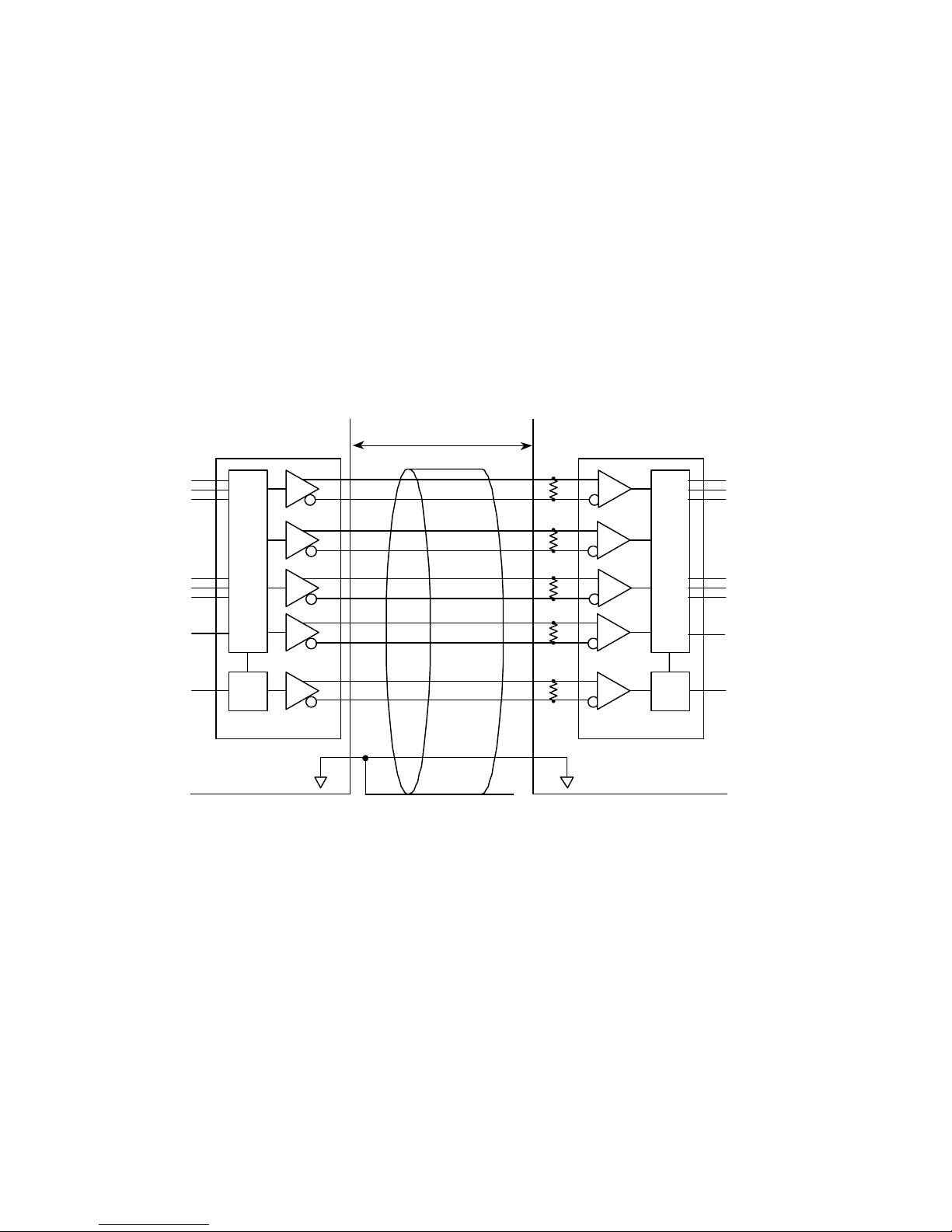
Channel Link Typical Application:
TxIN
LVCMOS/
LVTTL
25
26
27
/PD
TxCLK
TX
DS90CR287
0
1
2
PCB
LVDS Cable
(media dependent)
GND
SHIELD
RX
DS90CR288A
RxOUT
0
1
2
25
26
27
/PD
RxCLK
PCB
The diagram above illustrates the use of the Channel Link chipset (Tx/Rx). This
chipset is able to transmit 28 bits of LVTTL/LVCMOS data using four LVDS channels
for a total throughput of 2.38 Gbps (297.5 Mbytes/s).
Input clock rate is specified to be between 20 MHz to 85 MHz maximum. The
interconnect between the two devices may be a variety of media including: twisted
pair cables, twin-ax cables, and / or backplanes for example. Driving between the
two devices is a function of interconnect skew and clock rate. Distances up to ten
meters are possible at the lower clock rates and distances of 1 to 2 meters is
possible at the higher clock rates. Please refer to the chipset datasheet for more
information and parametric tables.
National Semiconductor Corporation
Interface Products
LIT# CLINK3V28BT-85-UM
Rev 2.1
Date: 10/12/2005
Page 4 of 28
Page 5

Channel Link Evaluation Kit User Manual
How to set up the Evaluation Kit:
The PCB routing for the Tx input pins (TxIN) have been laid out to accept incoming
data from a 60-pin IDC connector. The TxOUT/RxIN interface uses the 3M MDR
connector and Spectra Strip cable. This typical cable provides minimal skew
between LVDS channels and can typically support longer lengths than atwisted pair
cable. Please follow these steps to set up the evaluation kit for bench testing and
performance measurements:
1) Connect one end of the Spectra Strip cable to the transmitter board and the other
end to the receiver board. This is a standard pinout cable, longer lengths are
available for purchase from Alliance Technology – see www.alliancet.com
2) Jumpers have been configured at the factory, they should not require any
changes for operation of the chipset. See text on Jumper settings for more
details.
3) For the incoming data, connect a flat (ribbon) cable to the transmitter board to a
data source (signal generator, pattern generator, BERT tester, etc). Connect the
60-pin flat cable from the receiver board to the receiver load (BERT or other
equipment). Scope probes may also be connected directly to the pins if desired.
Mini-coax cable with headers on one end may also be used. This type of cable is
supplied with some test equipment. The 60-pin IDC equipment interface cable is
supplied with this kit which can be used to build custom cables.
4) Power for the Tx and Rx boards must be supplied externally through TP1 (Vcc).
Grounds for both boards are connected through TP2 (GND) (see section below).
5) Data applied to the inputs is now serialized, transmitted, deserialized and redriven at the receiver outputs.
This evaluation kit can also be used to evaluate the performance of other National
Semiconductor’s 28-bit and 21-bit Channel Link Serdes chipset. Simply replace the
existing DS90CR287/288A devices with a different 28-bit or 21-bit device chipset
and follow the above procedure. For evaluation of 21-bit device chipset, user needs
to pull TxIN[21:27] high or low.
Power Connection:
The Transmitter and Receiver boards must be powered by supplying power
externally through TP1 (Vcc) and TP2 (GND) on EACH board. Information on
maximum supply voltage can be found on device datasheet’s Absolute Maximum
Ratings section. The maximum voltage that should ever be applied to the Channel
Link Transmitter (DS90CR287) or Receiver (DS90CR288A) Vcc terminal is +4V
MAXIMUM.
National Semiconductor Corporation
Interface Products
LIT# CLINK3V28BT-85-UM
Rev 2.1
Date: 10/12/2005
Page 5 of 28
Page 6
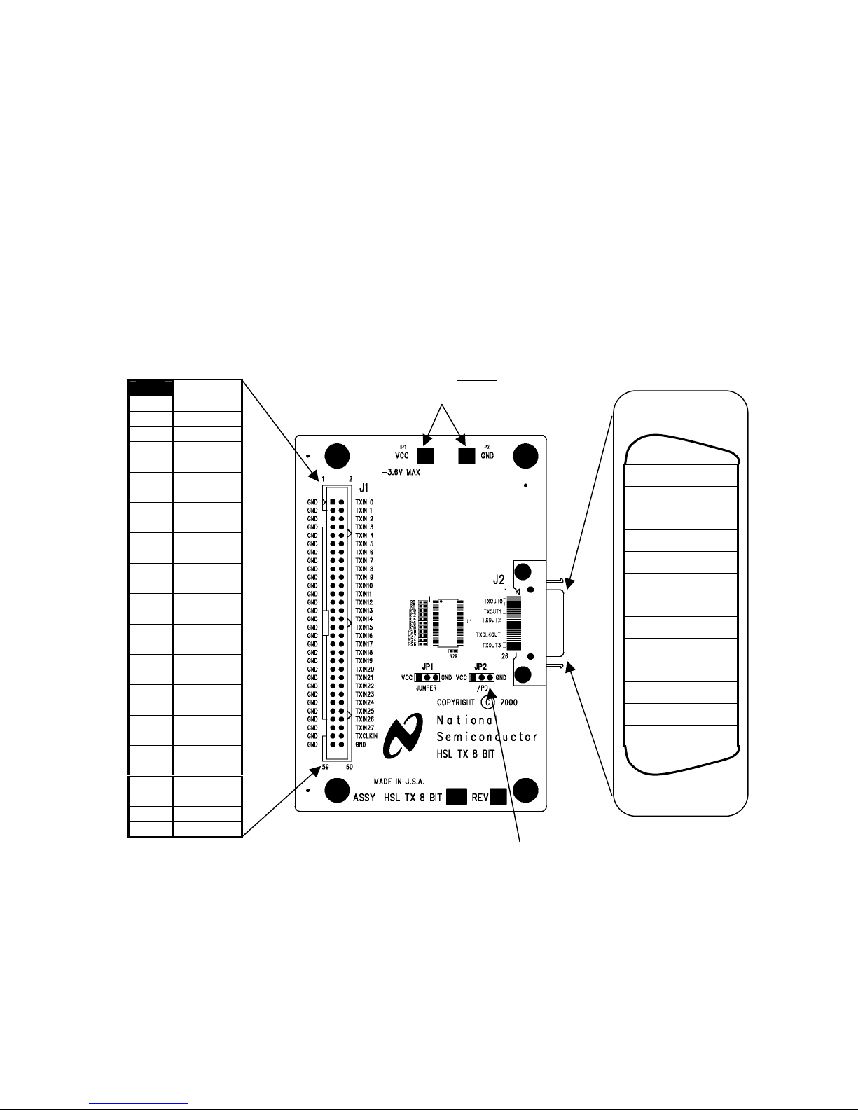
Channel Link Evaluation Kit User Manual
Channel Link Transmitter Board Description:
J1 (60 position) accepts 28 bit LVTTL/LVCMOS data, clock and also the PD* control
signal.
The Channel Link Transmitter board is powered externally. For the transmitter to be
operational, the Power Down pin must be set HIGH with a jumper.
The 3M MDR connector (J2) provides the interface for LVDS signals for the
Receiver board.
60-pin IDC Connector
1 2
GND
GND
GND
GND
GND
GND
GND
GND
GND
GND
GND
GND
GND
GND
GND
GND
GND
GND
GND
GND
GND
GND
GND
GND
GND
GND
GND
GND
GND
GND GND
TXIN0
TXIN1
TXIN2
TXIN3
TXIN4
TXIN5
TXIN6
TXIN7
TXIN8
TXIN9
TXIN10
TXIN11
TXIN12
TXIN13
TXIN14
TXIN15
TXIN16
TXIN17
TXIN18
TXIN19
TXIN20
TXIN21
TXIN22
TXIN23
TXIN24
TXIN25
TXIN26
TXIN27
TXCLKIN
59 60
J1
Vcc and Gnd MUST be
applied externally here
/PD
TxOUT LVDS signals
3M MDR connector
Pin 1
NC OUT0-
GND OUT0+
NC NC
OUT1- GND
OUT1+ NC
OUT2- GND
OUT2+ NC
NC NC
NC CLK-
GND CLK+
NC NC
OUT3- GND
OUT3+ NC
Pin 13
Pin 14
Pin 26
J2
Note: JP1 is not used
National Semiconductor Corporation
Interface Products
LIT# CLINK3V28BT-85-UM
Rev 2.1
Date: 10/12/2005
Page 6 of 28
Page 7

Channel Link Evaluation Kit User Manual
Jumper Settings for the Tx Board
Jumper Purpose Settings
/PD PowerDown = ON = OFF
(JP2) Vcc GND Vcc GND
(ON: Tx is operational; OFF: Tx powers down)
Default setting is JP2 set HIGH (to Vcc), operational mode.
National Semiconductor Corporation
Interface Products
LIT# CLINK3V28BT-85-UM
Rev 2.1
Date: 10/12/2005
Page 7 of 28
Page 8
Channel Link Evaluation Kit User Manual
0
0
3
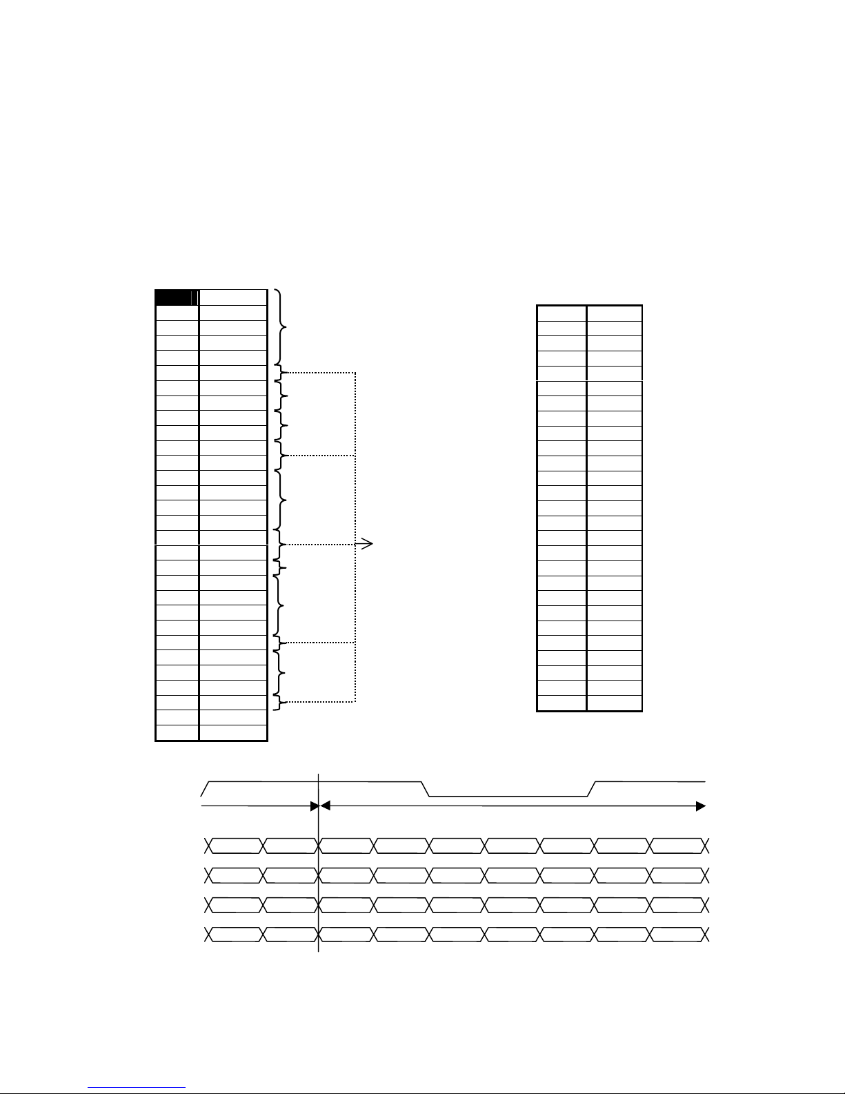
Tx LVDS Mapping by IDC Connector
The following two figures illustrate how the Tx inputs are mapped to the IDC
connector (J1) (Note – labels are also printed on the demo boards). The 26-pin
MDR connector pinout is also shown.
(Transmitter Board)
60-pin IDC Connector
Pin 1
GND
GND
GND
GND
GND
GND
GND
GND
GND
GND
GND
GND
GND
GND
GND
GND
GND
GND
GND
GND
GND
GND
GND
GND
GND
GND
GND
GND
GND
GND GND
TXIN0
TXIN1
TXIN2
TXIN3
TXIN4
TXIN5
TXIN6
TXIN7
TXIN8
TXIN9
TXIN10
TXIN11
TXIN12
TXIN13
TXIN14
TXIN15
TXIN16
TXIN17
TXIN18
TXIN19
TXIN20
TXIN21
TXIN22
TXIN23
TXIN24
TXIN25
TXIN26
TXIN27
TXCLKIN
J1
2
TXOUT
TXOUT
TXOUT1
TXOUT1
TXOUT1
TXOUT2
TXOUT2
60 59
TXOUT
TxOUT LVDS signals
3M MDR connector
PIN # NAME
1 NC
2
GND
3 NC
OUT1-
4
OUT1+
5
OUT2-
6
OUT2+
7
8 NC
9 NC
10
GND
11 NC
OUT3-
12
OUT3+
13
OUT0-
14
OUT0+
15
16 NC
17
GND
18 NC
19
GND
20 NC
21 NC
CLK-
22
CLK+
23
24 NC
25
GND
26 NC
J2
TXCLKOUT
Previous Cycle
TXOUT3
TXOUT2
TXOUT1
TXOUT0
Parallel LVTTL/LVCMOS Data Inputs Mapped to LVDS Outputs
TXIN23 TXIN17 TXIN16 TXIN11 TXIN10 TXIN5 TXIN27
TXIN26 TXIN25 TXIN24 TXIN22 TXIN21 TXIN20 TXIN19
TXIN18 TXIN15 TXIN14 TXIN13 TXIN12 TXIN9 TXIN8
TXIN7 TXIN6 TXIN4 TXIN3 TXIN2 TXIN1 TXIN0
Next Cycle
LIT# CLINK3V28BT-85-UM
National Semiconductor Corporation
Interface Products
Rev 2.1
Date: 10/12/2005
Page 8 of 28
Page 9
Channel Link Evaluation Kit User Manual
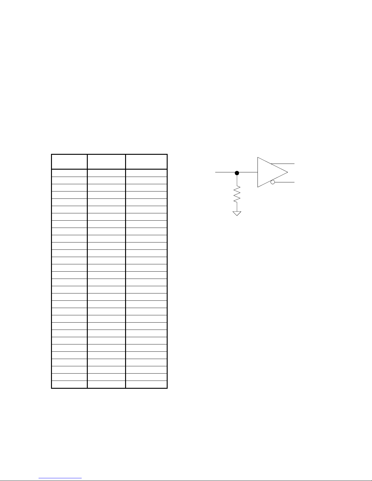
Tx Board Options: 50 Ohm Termination for TxIN
On the Tx demo board, the 29 inputs have an option for 50 Ohm terminations.
There are 0402 pads for this purpose. One side is connected to the signal line and
the other side is tied to ground. These pads are unpopulated from the factory but
are provided if the user needs to install a 50 Ohm termination. R1 TO R28 are
associated with the Tx data input lines. R29 is associated with CLKIN. Some test
equipment may require a 50 Ohm load.
Mapping of Transmitter Inputs for the Optional Termination Resistors is shown
below:
Tx Pin
Names
TxIN0 51 R1
TxIN1 52 R2
TxIN2 54 R3
TxIN3 55 R4
TxIN4 56 R5
TxIN5 2 R6
TxIN6 3 R7
TxIN7 4 R8
TxIN8 6 R9
TxIN9 7 R10
TxIN10 8 R11
TxIN11 10 R12
TxIN12 11 R13
TxIN13 12 R14
TxIN14 14 R15
TxIN15 15 R16
TxIN16 16 R17
TxIN17 18 R18
TxIN18 19 R19
TxIN19 20 R20
TxIN20 22 R21
TxIN21 23 R22
TxIN22 24 R23
TxIN23 25 R24
TxIN24 27 R25
TxIN25 28 R26
TxIN26 30 R27
TxIN27 50 R28
TxCLKIN 31 R29
Tx Pin
Number
Termination
Resistor
TX
50 Ohm Termination
(Optional)
National Semiconductor Corporation
Interface Products
LIT# CLINK3V28BT-85-UM
Rev 2.1
Date: 10/12/2005
Page 9 of 28
Page 10

Channel Link Evaluation Kit User Manual
BOM (Bill of Materials) Transmitter PCB:
HSL Demo Board Schematic REV1
HSL8TXR1 Revision: 1 Channel Link
Item Qty Reference Part Pkg Size
1 1 C1
10 µF
CASE D
2 4 C2,C6,C10,C14
3 4 C3,C7,C11,C15
4 3 C4,C8,C12
5 3 C5,C9,C13
6 2 JP2 3_PIN_HEADER 0.1" spacing
7 1 J1 IDC30X2 IDC60
8 1 J2 3M_MDR 26MDR
9 29 R1,R2,R3,R4,R5,R6,R7,R8, Optional 0402 PAD
R9,R10,R11,R12,R13,R14,
R15,R16,R17,R18,R19,R20,
R21,R22,R23,R24,R25,R26,
R27,R28,R29
10 8 R30,R32,R33,R34,R35, 0 Ohm 0402
R36,R37
11 2 TP1,TP2 N/A TP_.2"X.2"
12 1 U1 DS90CR287MTD 56-pin TSSOP
0.1 µF
22 µF
0.001 µF
0.01 µF
1206 (3216)
7343 (D)
0805 (2012)
0805 (2012)
National Semiconductor Corporation
Interface Products
LIT# CLINK3V28BT-85-UM
Rev 2.1
Date: 10/12/2005
Page 10 of 28
Page 11

Channel Link Evaluation Kit User Manual
Rx Channel Link Receiver Board:
J1 (60 position) provides access to the 28 bit LVTTL/LVCMOS, clock outputs.
The Channel Link Receiver board is powered from the pads show below. For the
receiver to be operational, the Power Down pin must be set HIGH with the jumper.
The 3M MDR connector (J2) provides the interface for LVDS signals for the
Receiver board.
RxIN LVDS signals
3M MDR26-7 connector
Pin 26
NC IN0-
GND IN0+
NC NC
IN1- GND
IN1+ NC
IN2- GND
IN2+ NC
NC NC
NC CLK-
GND CLK+
NC NC
IN3- GND
IN3+ NC
Pin 14
Pin 13
Pin 1
J2
Vcc and Gnd MUST be
applied externally here
/PD
60 59
RXOUT27
RXOUT26
RXOUT25
RXOUT24
RXOUT23
RXOUT22
RXOUT21
RXOUT20
RXOUT19
RXOUT18
RXOUT17
RXOUT16
RXOUT15
RXOUT14
RXOUT13
RXOUT12
RXOUT11
RXOUT10
RXOUT9
RXOUT8
RXOUT7
RXOUT6
RXOUT5
RXOUT4
RXOUT3
RXOUT2
RXOUT1
RXOUT0
RXCLKOUT
GND
GND
GND
GND
GND
GND
GND
GND
GND
GND
GND
GND
GND
GND
GND
GND
GND
GND
GND
GND
GND
GND
GND
GND
GND
GND
GND
GND
GND
GND
GND
2 1
National Semiconductor Corporation
Interface Products
LIT# CLINK3V28BT-85-UM
Rev 2.1
Date: 10/12/2005
Page 11 of 28
Page 12

Channel Link Evaluation Kit User Manual
Selectable Jumper Settings for the Rx Board
Jumper Purpose Settings
/PD PowerDown = ON = OFF
(JP1) Vcc GND Vcc GND
(ON: Rx is operational; OFF: Rx powers down)
Default setting is JP1 set HIGH (to Vcc), operational mode.
National Semiconductor Corporation
Interface Products
LIT# CLINK3V28BT-85-UM
Rev 2.1
Date: 10/12/2005
Page 12 of 28
Page 13

Channel Link Evaluation Kit User Manual
0
0
LVDS Mapping by IDC Connector
The following two figures illustrate how the Rx outputs are mapped to the IDC
connector (J1) (Note – labels are also printed on the demo boards). The 26-pin
MDR connector pinout is also shown.
(Receiver Board)
RXIN3
RXIN2
RXIN2
RXIN1
RXIN1
RXIN1
RXIN
RXIN
60-pin IDC Connector
60 59
2
RXOUT27
RXOUT26
RXOUT25
RXOUT24
RXOUT23
RXOUT22
RXOUT21
RXOUT20
RXOUT19
RXOUT18
RXOUT17
RXOUT16
RXOUT15
RXOUT14
RXOUT13
RXOUT12
RXOUT11
RXOUT10
RXOUT9
RXOUT8
RXOUT7
RXOUT6
RXOUT5
RXOUT4
RXOUT3
RXOUT2
RXOUT1
RXOUT0
RXCLKOUT
GND
GND
GND
GND
GND
GND
GND
GND
GND
GND
GND
GND
GND
GND
GND
GND
GND
GND
GND
GND
GND
GND
GND
GND
GND
GND
GND
GND
GND
GND
GND
J1
Pin 1
RxIN LVDS signals
3M MDR connector
PIN # NAME
1 NC
2
GND
3 NC
CLK+
4
CLK-
5
6 NC
7 NC
8
GND
9 NC
10
GND
11 NC
IN0+
12
IN0-
13
IN3+
14
IN3-
15
16 NC
17
GND
18 NC
19 NC
IN2+
20
IN2-
21
IN1+
22
IN1-
23
24 NC
25
GND
26 NC
J2
RXCLKIN
Previous Cycle Next Cycle
RXIN3
RXIN2
RXIN1
RXIN0
LVDS Data Inputs Mapped to LVTTL/LVCMOS Outputs
RXOUT23 RXOUT17 RXOUT16 RXOUT11 RXOUT10 RXOUT5 RXOUT27
RXOUT26 RXOUT25 RXOUT24 RXOUT22 RXOUT21 RXOUT20 RXOUT19
RXOUT18 RXOUT15 RXOUT14 RXOUT13 RXOUT12 RXOUT9 RXOUT8
RXOUT7 RXOUT6 RXOUT4 RXOUT3 RXOUT2 RXOUT1 RXOUT0
LIT# CLINK3V28BT-85-UM
National Semiconductor Corporation
Interface Products
Rev 2.1
Date: 10/12/2005
Page 13 of 28
Page 14

Channel Link Evaluation Kit User Manual
(Op
)
Rx Optional: Series Termination for RxOut
On the Rx demo board, there are 29 outputs that have an 0402 pad in series (which
are shorted out). These pads are unpopulated from the factory but are provided if
the user needs to install a 450 Ohm series resistors. This is required if directly
connecting to 50 Ohm inputs on a scope. To use this option the user must cut the
signal line between the pads before installing the 450 Ohm series resistors. R1 to
R28 are associated with the DATA output lines. R29 is associated with CLKOUT.
The total load presented to the receiver output is 500 Ohms (450 + 50). The
waveform on the scope is 1/10 of the signal due to the resulting voltage divider (50 /
(450 + 50)).
Optional Series Termination Resistor mapping is shown below:
Rx Pin Names Rx Pin
Number
RxOUT0 27 R28
RxOUT1 29 R27
RxOUT2 30 R26
RxOUT3 32 R25
RxOUT4 33 R24
RxOUT5 34 R23
RxOUT6 35 R22
RxOUT7 37 R21
RxOUT8 38 R20
RxOUT9 39 R19
RxOUT10 41 R18
RxOUT11 42 R17
RxOUT12 43 R16
RxOUT13 45 R15
RxOUT14 46 R14
RxOUT15 47 R13
RxOUT16 49 R12
RxOUT17 50 R11
RxOUT18 51 R10
RxOUT19 53 R9
RxOUT20 54 R8
RxOUT21 55 R7
RxOUT22 1 R6
RxOUT23 2 R5
RxOUT24 3 R4
RxOUT25 5 R3
RxOUT26 6 R2
RxOUT27 7 R1
RxCLKOUT 26 R29
Series
Termination
Resistor
RX
Series Termination
tional
National Semiconductor Corporation
Interface Products
LIT# CLINK3V28BT-85-UM
Rev 2.1
Date: 10/12/2005
Page 14 of 28
Page 15

Channel Link Evaluation Kit User Manual
BOM (Bill of Materials) Receiver PCB:
HSL Demo Board Schematic REV1
HSL8RXR1 Revision: 1 Channel Link
Item Qty Reference Part Pkg Size
1 1 C1
10 µF
CASE D
2 4 C2,C6,C10,C14
3 4 C3,C7,C11,C15
4 3 C4,C8,C12
5 3 C5,C9,C13
6 1 JP1 3_PIN_HEADER 0.1" spacing
7 1 J1 IDC30X2 IDC60
8 1 J2 3M_MDR 26MDR
9 29 R1,R2,R3,R4,R5,R6,R7,R8, Optional 0402 PAD
R9,R10,R11,R12,R13,R14, (See previous page)
R15,R16,R17,R18,R19,R20,
R21,R22,R23,R24,R25,R26,
R27,R28,R29
6 R35,R36,R37,R38,R39,R40 0 Ohm 0402
0.1 µF
22 µF
0.001 µF
0.01 µF
1206 (3216)
7343 (D)
0805 (2012)
0805 (2012)
10 5 R30,R31,R32,R33,R34 100 Ohm 0402
11 2 TP1,TP2 N/A TP_.2"X.2"
12 1 U1 DS90CR288AMTD 56-pin TSSOP
National Semiconductor Corporation
Interface Products
LIT# CLINK3V28BT-85-UM
Rev 2.1
Date: 10/12/2005
Page 15 of 28
Page 16

Channel Link Evaluation Kit User Manual
Typical Connection / Test Equipment
The following is a list of typical test equipment that may be used to generate signals
for the TX inputs:
1) TEK HFS9009 - This pattern generator along with 9DG2 Cards may be used to
generate input signals and also the clock signal.
2) TEK DG2020 - This generator may also be used to generate data and clock
signals.
3) TEK MB100 BERT - This bit error rate tester may be used for both signal source
and receiver.
4) Any other signal / pattern generator that generates the correct input levels as
specified in the datasheet.
The following is a list of typically test equipment that may be used to monitor the
output signals from the RX:
1) TEK MB100 BERT - Receiver.
2) Any SCOPE with 50 Ohm inputs or high impedance probes.
LVDS signals may be easily measured with high impedance / high bandwidth
differential probes such as the TEK P6247 or P6248 differential probes.
The picture below shows a typical test set up using a generator and scope.
Signal/Pattern Generator,
BERT Tester
50 ohm
Optional
Receiver
Board
Termination
450 ohm
50 ohm
50 ohm
Transmitter
Board
LVDS Interface
Cable
Optional
Termination
Typical Connection / Test Equipment Setup
National Semiconductor Corporation
Interface Products
50 ohm
Oscilloscope,
BERT Tester
LIT# CLINK3V28BT-85-UM
Rev 2.1
Date: 10/12/2005
Page 16 of 28
Page 17

Channel Link Evaluation Kit User Manual
Typical Waveshapes
LVDS
The plot above shows both the LVDS Data channel with PRBS data and also the
LVDS Clock over laid. Note that the clock pattern is 4 bit times HIGH and 3 bit times
LOW. The differential signal should be typically +/-300mV. These waveforms were
acquired using the TEK P6248 Probes. Clock rate is 85MHz.
National Semiconductor Corporation
Interface Products
LIT# CLINK3V28BT-85-UM
Rev 2.1
Date: 10/12/2005
Page 17 of 28
Page 18

RxOUT
Channel Link Evaluation Kit User Manual
The plot above shows both the recovered PRBS data and also the regenerated
Clock overlaid. Note that the clock transitions slightly before the data transition and
strobes the data on the rising edge of the clock. The data and clock signals are low
drive 3V CMOS outputs. The plot above is at 85MHz.
National Semiconductor Corporation
Interface Products
LIT# CLINK3V28BT-85-UM
Rev 2.1
Date: 10/12/2005
Page 18 of 28
Page 19

Channel Link Evaluation Kit User Manual
Troubleshooting
If the demo boards are not performing properly, use the following as a guide for
quick solutions to potential problems. If the problem persists, please contact the
Interface Applications hotline number (+1 408 721 8500) for assistance.
QUICK CHECKS:
1. Check that Power and Ground are connected to both Tx AND Rx boards.
2. Check the supply voltage (typical 3.3V) and also current draw with both Tx and
Rx boards (should be about 200mA with clock and one data bit at 66MHz).
3. Verify input clock and input data signals meet requirements (VIL, VIH, tset,
thold), Also verify that data is strobed on the rising edge of the clock.
4. Check that the Jumpers are set correctly.
5. Check that the 2 meter cable is properly connected.
TROUBLESHOOTING CHART
Problem…
There is only the output clock.
There is no output data.
Solution…
Make sure the data is applied to the correct input pin.
Make sure data is valid at the input.
No output data and clock. Make sure Power is on. Input data and clock are
active and connected correctly.
Make sure that the 2 meter cable is secured to both
demo boards.
Power, ground, input data and
input clock are connected
correctly, but no outputs.
The devices are pulling more
than 1A of current.
After powering up the demo
boards, the power supply
reads less than 3V when it is
Check the Power Down pins of both boards and
make sure that the devices are enabled (/PD=Vcc) for
operation.
Check for shorts in the cables connecting the TX and
RX boards.
Use a larger power supply that will provide enough
current for the demo boards, a 500mA power supply
is recommended.
set to 3.3V.
National Semiconductor Corporation
Interface Products
LIT# CLINK3V28BT-85-UM
Rev 2.1
Date: 10/12/2005
Page 19 of 28
Page 20

Channel Link Evaluation Kit User Manual
Additional Information
For more information on Channel Link Transmitters/Receivers, refer to the National’s
LVDS website at:
www.national.com/appinfo/lvds
Application Notes
• AN-1041 Channel Link Moving and Shaping Information in Point-to-Point
Applications
• AN-971 An Overview of LVDS technology
• AN-977 LVDS Signal Quality: Jitter Measurement Using Eye Pattern
• AN-1059 High Speed Transmission with LVDS Devices
• AN-1108 Channel-Link PCB and Interconnect Design-In Guidelines
Interface Applications Hotline:
The Interface Hotline number is: +1 408 721-8500
National Semiconductor Corporation
Interface Products
LIT# CLINK3V28BT-85-UM
Rev 2.1
Date: 10/12/2005
Page 20 of 28
Page 21

Channel Link Evaluation Kit User Manual
Appendix
Cable and connector
The next few pages provide a full description of the cable and connector.
For product request please contact 3M and Alliance Technology Enterprise.
3M Connector Data is available at: www.mmm.com/Interconnects
Spectra Strip Cable Data is available at: www.alliancet.com
Tx PCB Schematic
Transmitter Board: HSL Demo Board Schematic
Document Number: HSL8TX
Rev: 1.0
Rx PCB Schematic
Receiver Board: HSL Demo Board Schematic
Document Number: HSL8RX
Rev: 1.0
National Semiconductor Corporation
Interface Products
LIT# CLINK3V28BT-85-UM
Rev 2.1
Date: 10/12/2005
Page 21 of 28
Page 22

.050″ Mini D Ribbon (MDR) Connectors
Surface Mount Right Angle Receptacle — Shielded 102XX-1210VE Series
140
Physical
Shr
Insulation
Material: Glass
Flammability:
Color: Beige
Contact
Material:
Plating
Underplate:
W
iping Area:
oud and Latch Hook
Material: Steel
Plating: Nickel
Scr
ew Lock
Material:
Plating: Tin
Marking:
IMPORTANT
ALL STATEMENTS, TECHNICAL INFORMATION AND RECOMMENDATIONS
CONTAINED
THE ACCURACY OR COMPLETENESS THEREOF IS NOT GUARANTEED, AND
THE
PLIED:
SELLER’S
SUCH QUANTITY OF THE PRODUCT PROVED TO BE DEFECTIVE. NEITHER
SELLER
DAMAGE,
INABILITY TO USE THE PRODUCT
THE SUITABILITY OF THE PRODUCT FOR HIS INTENDED USE, AND USER ASSUMES
NO STATEMENT OR RECOMMENDATION NOT CONTAINED HEREIN SHALL
HAVE ANY FORCE OR EFFECT UNLESS IN AN AGREEMENT SIGNED BY OFFICERS OR SELLER AND MANUFACTURER.
Date Issued: February 5, 1998
HEREIN ARE BASED ON TESTS WE BELIEVE T
FOLLOWING IS
NOR MANUF
ALL RISK AND LIABILITY WHA
MADE IN LIEU OF ALL W
AND MANUF
DIRECT OR CONSEQUENTIAL, ARISING OUT OF THE USE OF OR THE
ACTURER SHALL
Reinforced Polyester (PCT)
UL 94V
-0
Copper Alloy (C521)
80 µ″ [2.0 µm] Nickel — QQ-N-290, Class 2
20 µ″ [0.50 µm] Min Gold — MIL-G-45204, T
Copper Alloy (C521)
3M Logo and Part Number
NOTICE T
ACTURER’S ONLY OBLIGA
. BEFORE USING, USER SHALL DETERMINE
O PURCHASER
ARRANTIES, EXPRESSED OR IM
BE LIABLE FOR ANY INJURY, LOSS OR
TSOEVER IN CONNECTION THEREWITH.
ype II, Grade C
O BE RELIABLE,
TION SHALL BE T
BUT
O REPLACE
TS-0755-05
1 of 3
Sheet
-
Electrical
Curr
ent Rating:
Insulation Resistance:
W
ithstanding V
oltage:
1 A
> 5 × 10⁸Ω at
500 V
Environmental
Temperatur
UL File No.: E68080
3M Electronic Products Division
6801 River Place Blvd.
Austin, TX 78726-9000
e Rating:
Process:
–55°
Surface mount compatible up to 240°C peak for short durations.
500 VDC
rms for 1 Minute
C to +105
°C
For
technical, sales or ordering information call
800-225-5373
Page 23

.050″ Mini D Ribbon (MDR) Connectors
Contact
3M Part
Surface Mount Right Angle Receptacle — Shielded 102XX-1210VE Series
Contact 3M Part
Quantity
20
26
40
2X M2.5 Thread
.394
[ 10.00 ]
.203
[ 5.15 ]
Number
10220-1210
10226-1210
10240-1210
[ 3.5 ]
VE
VE
VE
position above
last position
last position
.138
Dimensions
A.008 B.006 C.006 D.006 E.006
1.32 [ 33.4 ] 1.081 [ 27.45 ] .650 [ 16.51 ] .475 [ 12.07 ] .646 [ 16.4 ]
1.50 [ 38.2 ] 1.231 [ 31.26 ] .800 [ 20.32 ] .625 [ 15.88 ] .795 [ 20.2 ]
1.85 [ 47.1 ] 1.581 [ 40.15 ] 1.150 [ 29.21 ] .975 [ 24.77 ] 1.150 [ 29.2 ]
A
position
D
.025 [ 0.635 ]
position 2
.010 nom.
[ 0.25 ]
E
below pos. 1
position 1
.19
[ 4.8 ]
.368
[ 9.35 ]
.047
1.20 ]
[
[ 4.75 ]
.187
(see note in ordering info)
.248
[ 6.30 ]
last position
Ordering Information
2X M2.5 Thread
B
Position 1
C
102XX-1210VE
Contact Quantity
(See T
able)
.189 [ 4.80 ]
Position
Positioning Boss (2x)
Inch
[mm]
T
olerance Unless Noted
.0 .00 .000
±
.1± .01
Inch
[ ] Dimensions for
Reference only
±
.005
Note:
Use (M2.5x8mm) screws to mount to panel with max. thickness of 2.0 mm.
3M
Electronic Products Division
6801 River Place Blvd.
Austin, TX 78726-9000
TS-0755-05
Sheet
For
technical, sales or ordering information call
800-225-5373
2 of 3
Page 24

.050″ Mini D Ribbon (MDR) Connectors
Contact
Contact
Surface Mount Right Angle Receptacle — Shielded 102XX-1210VE Series
Contact
Quantity
20 1.081 [ 27.45 ] .650 [ 16.51 ] .475 [ 12.07 ]
26 1.230 [ 31.26 ] .800 [ 20.32 ] .625 [ 15.88 ]
40 1.581 [ 40.15 ] 1.150 [ 29.21 ] .975 [ 24.77 ]
Dimensions
A ± .002 B ± .002 C ± .002
.122 [ 3.1 ]
.138 [ 3.5 ]
.256 [ 6.5 ]
PCB Ref. Edge
center
spacing
.025 ±
.0008
.118 [ 3.0 ]
Recommended Board Layout
(viewed
from connector side)
center spacing
C
.088 [ 2.223 ]
B
A
.165 [ 4.2 ]
Solder Tail Layout Detail
(#’s Correspond to Connector Contact # Shown on Previous Page)
20 Pos.
Last
Pos.
10 9 8 7
20
19 18 17 16 15 14 13 12 11
654321
PCB Ref. Edge
Connector Position
(T
op Row)
Position
(Bottom Row)
.187 max.
[ 4.75 ]
Solder Pads for
Solder T
below for more detail)
.016 ±
.0004
.093 ±
.0004
Positioning
ail (See
.110±
.004 (2X)
Screw Lock
(see notes below)
Lockstand Solder
Pad Outline
.079 + .004 (2X)
– .000
Hole
13 12 11
10987
26 Pos.
Last
Pos.
26 25 24
19 18 17 16 15 14 13 12
23
40 Pos.
402039 38 37 36 35 34 33 32 31
Last
Pos.
Contact
Quantity
20 .94 [ 23.8 ] 1.081 [ 27.45 ]
26 1.09 [ 27.6 ] 1.231 [ 31.26 ]
40 1.44 [ 36.5 ] 1.581 [ 40.15 ]
**Notes:
1.
Plated through holes for .062″ board thickness.
2. Use mounting screws ( M2.5 ) to fasten to board.
Dimensions
D E
654321
22 21 20 19 18 17 16 15 14
PCB
Ref. Edge
10 9 8 7
11
30
29 28 27 26 25 24 23 22 21
PCB Ref. Edge
Recommended
Note: Panel thickness .079 [ 2.00 ] Max.
R .060
[ 1.50 ]
Connector
(T
Position
(Bottom
654321
Position (Bottom Row)
Position
op Row)
Row)
Connector Position
Panel Cut-out
D ± .004
E ± .004
.319 ± .004
8.1 ]
[
TS-0755-05
Sheet 3 of 3
3M
Electronic Products Division
6801 River Place Blvd.
Austin, TX 78726-9000
For
technical, sales or ordering information call
800-225-5373
Page 25

Cable Assembly Part number MDR26-5-6.5
MDR26-5-6.5
3M mdr 10126-6000 3Mmdr 10126-6000
Part number
2 meters
Spectra Strip cable
Skew Clear twin ax
Cable length
Connector type 6.5 Ft 2 meter
Number of twin-Ax pairs
Connector number of positions
26
Cable assemby ordering information.
Alliance Technology Enterprise
521 Central Ave Suite B
Menlo Park CA 94025
650 329 8554
info@allianceT.com
www.AllianceT.com
5
Page 26

National Semiconductor Channel Link Cable Assembley Pinout
MDR26-5-6.5C
Alliance Technology part number
Pin Assignment Pin Assignment
Side A Side B
3M Mdr Part 3M Mdr Part
10126-6000 10126-6000
1 No Connect 26 No Connect
2 TxOut0Gnd+ 25 TxOutGnd3 No Connect 24 No Connect
4 TxOut1- 23 RxIn1 5 TxOut1+ 22 RxIn1 +
6 TxOut2- 21 RxIn2 7 TxOut2+ 20 RxIn2 +
8 Reserved 19 Reserved
9 No Connect 18 No Connect
10 TxClkoutGnd 17 RxInClkGnd
11 No Connect 16 No Connect
12 TxOut3- 15 RxIn3 13 Txout3+ 14 Rxin3 +
14 TxOut0- 13 RxIn0 15 TxOut0+ 12 Rxin0 +
16 No Connect 11 No Connect
17 TxOut1Gnd 10 RxIn1Gnd
18 No Connect 9 No Connect
19 TxOut2gnd 8 Rxin2Gnd
20 Reserved 7 Reserved
21 Reserved 6 Reserved
22 TxClkOut- 5 RxClkIn 23 TxClkOut+ 4 RxClkIn +
24 No Connect 3 No Connect
25 TxOut3Gnd 2 RxIn3Gnd
26 No Connect 1 No Connect
Pin 1 Pin 13
Pin 14 Pin 26
Cable assembly
Page 27

/PD
+3.6V MAX
+3.6V MAX
HSL8TX
HSL Demo Board Schematic
1 1Monday, August 21, 2000
1
Title
Size Document Number Rev
Date: Sheet
of
VCC1
LVDS_VCC
LVDS_GND
VCC1
PLL_VCC
PLL_GND
TXIN12
TXIN23
TXIN8
TXIN6
TXIN14
TXIN24
TXIN19
TXIN5
TXIN10
TXIN21
TXIN11
TXIN22
TXIN9
TXIN15
TXIN13
TXIN7
TXIN18
TXIN25
TXOUT3+
PLL_GND
TXOUT3-
PLL_VCC
TXOUT2+
PLL_VCC
TXCLKOUT-
TXOUT1+
PLL_GND
LVDS_GND
TXOUT0TXOUT0+
TXCLKOUT+
LVDS_VCC
LVDS_VCC
TXOUT2-
TXOUT1-
LVDS_GND
GND1
GND1
TXIN22
TXIN12
TXIN3
TXIN21
TXIN4
GND
TXIN10
TXIN18
TXIN17
TXIN16
TXIN6
TXIN0
TXIN1
TXIN0
TXIN4
TXIN20
TXIN3
TXIN25
TXIN8
TXIN27
TXIN26
TXIN26
TXIN1
TXIN19
TXIN11
TXIN24
TXIN7
GND
TXIN15
TXIN14
TXIN9
TXCLKIN
TXIN27
TXIN23
TXIN2
TXIN5
TXIN13
TXIN2
TXIN16
TXIN17
TXCLKIN
TXIN20
VCC
VCC
VCC
VCC
VCC
+
C1
10uF
TP1
TP_.2"X.2"
TP2
TP_.2"X.2"
C12
0.001uF
C9
0.01uF
C15
22uF
C4
0.001uF
C6
0.1uF
C14
0.1uF
C8
0.001uF
C10
0.1uF
C5
0.01uF
C13
0.01uF
C11
22uF
C7
22uF
C3
22uF
+
C2
0.1uF
R32
R36
R33
R37
R35
R34
R23
R12
R17
J2
3M_MDR_EZ8B
1
14
2
15
3
16
4
17
5
18
6
19
7
20
8
21
9
22
10
23
11
24
12
25
13
26
27
28
NC
TXOUT0TXOUT0GND
TXOUT0+
NC
NC
TXOUT1TXOUT1GND
TXOUT1+
NC
TXOUT2TXOUT2GND
TXOUT2+
NC
NC
NC
NC
TXCLKOUTTXCLKOUTGND
TXCLKOUT+
NC
NC
TXOUT3TXOUT3GND
TXOUT3+
NC
MOUNTING
MOUNTING
R18
R7
R16
R5
R21
R2
R13
R27
R11
R1
R24
R3
R28
R6
R14
R4
R19
R20
R25
R9
R15
R22
R29
R10
R8
R26
J1
IDC30X2
1 2
3 4
5 6
7 8
9 10
11 12
13 14
15 16
17 18
19 20
21 22
23 24
25 26
27 28
29 30
31 32
33 34
35 36
37 38
39 40
41 42
43 44
45 46
47 48
49 50
51 52
53 54
55 56
57 58
59 60
U1
DS90CR287
17
18
19
20
21
22
23
24
25
26
27
28 29
30
31
32
33
34
35
36
37
38
39
40
41
42
43
44
45
46
47
48
2
13
14
15
16
3
4
5
6
7
8
9
10
11
12
1
49
50
51
52
53
54
55
56
VCC
TXIN17
TXIN18
TXIN19
GND
TXIN20
TXIN21
TXIN22
TXIN23
VCC
TXIN24
TXIN25 GND
TXIN26
TXCLK IN
/PWR DWN
PLL GND
PLL VCC
PLL GND
LVDS GND
TXOUT3+
TXOUT3-
TXCLK OUT+
TXCLK OUT-
TXOUT2+
TXOUT2-
LVDS GND
LVDS VCC
TXOUT1+
TXOUT1-
TXOUT0+
TXOUT0-
TXIN5
GND
TXIN14
TXIN15
TXIN16
TXIN6
TXIN7
GND
TXIN8
TXIN9
TXIN10
VCC
TXIN11
TXIN12
TXIN13
VCC
LVDS GND
TXIN27
TXIN0
TXIN1
GND
TXIN2
TXIN3
TXIN4
R30
JP2
3_PIN_HEADER
Page 28

/PD
+3.6V MAX
+3.6V MAX
HSL8RX
HSL Demo Board Schematic
1 1Monday, August 21, 2000
1
Title
Size Document Number Rev
Date: Sheet
of
LVDS_VCC
PLL_VCC
VCC1
LVDS_GND
VCC1
PLL_GND
LVDS_VCC
PLL_VCC
PLL_GND
PLL_VCC
PLL_GND
LVDS_VCC
RXIN3+
GND1
RXIN1+
RXCLKIN-
RXIN1-
RXIN0-
LVDS_GND
RXIN0+
RXIN3-
GND1
RXCLKIN+
RXIN2+
RXIN2-
RXOUT11
RXOUT9
RXOUT20
RXOUT6
RXOUT24
RXOUT23
RXOUT1
RXOUT2
RXOUT8
RXOUT0
RXOUT7
RXOUT21
RXOUT5
RXCLKOUT
RXOUT13
RXOUT19
RXOUT0
RXOUT10
RXCLKOUT
RXOUT18
RXOUT17
RXOUT16
RXOUT25
RXOUT22
RXOUT3
RXOUT4
RXOUT12
RXOUT27
RXOUT26
RXOUT15
RXOUT14
RXOUT2
RXOUT3
RXOUT1
RXOUT19
RXOUT6
RXOUT17
RXOUT20
RXOUT15
RXOUT11
RXOUT9
RXOUT14
RXOUT5
RXOUT26
RXOUT10
RXOUT23
RXOUT18
RXOUT27
RXOUT21
RXOUT12
RXOUT24
RXOUT16
RXOUT13
RXOUT4
RXOUT8
RXOUT25
RXOUT7
RXOUT22
GND
GND
LVDS_GND
VCC
VCC
VCC
VCC
VCC
TP1
TP_.2"X.2"
R36
R37
R13
C12
0.001uF
C8
0.001uF
R17
R27
R20
R24
C3
22uF
R35
R22
C4
0.001uF
C6
0.1uF
R25
C10
0.1uF
C14
0.1uF
C9
0.01uF
R19
R21
R7
C15
22uF
C11
22uF
C7
22uF
C5
0.01uF
R15
C13
0.01uF
R32
100
R40
R39
R33
100
TP2
TP_.2"X.2"
+
C1
10uF
R30
100
R31
100
R38
+
C2
0.1uF
R34
100
J2
3M_MDR_EZ8B
26
13
25
12
24
11
23
10
22
9
21
8
20
7
19
6
18
5
17
4
16
3
15
2
14
1
27
28
NC
RXIN0-
RXIN0GND
RXIN0+
NC
NC
RXIN1-
RXIN1GND
RXIN1+
NC
RXIN2-
RXIN2GND
RXIN2+
NC
NC
NC
NC
RXCLKIN-
RXCLKINGND
RXCLKIN+
NC
NC
RXIN3-
RXIN3GND
RXIN3+
NC
MOUNTING
MOUNTING
R5
R6
R18
R4
R8
R23
R26
U1
DS90CR288
17
18
19
20
21
22
23
24
25
26
27
28 29
30
31
32
33
34
35
36
37
38
39
40
41
42
43
44
45
46
47
48
2
13
14
15
16
3
4
5
6
7
8
9
10
11
12
1
49
50
51
52
53
54
55
56
RXCLK INRXCLK IN+
RXIN3RXIN3+
LVDS GND
PLL GND
PLL VCC
PLL GND
/PWR DWN
RXCLK OUT
RXOUT0
GND RXOUT1
RXOUT2
VCC
RXOUT3
RXOUT4
RXOUT5
RXOUT6
GND
RXOUT7
RXOUT8
RXOUT9
VCC
RXOUT10
RXOUT11
RXOUT12
GND
RXOUT13
RXOUT14
RXOUT15
VCC
RXOUT23
LVDS VCC
LVDS GND
RXIN2RXIN2+
RXOUT24
GND
RXOUT25
RXOUT26
RXOUT27
LVDS GND
RXIN0RXIN0+
RXIN1RXIN1+
RXOUT22
RXOUT16
RXOUT17
RXOUT18
GND
RXOUT19
RXOUT20
RXOUT21
VCC
R28
R29
R3
R1
R2
R9
R14
R10
R12
R11
R16
J1
IDC30X2
12
34
56
78
910
1112
1314
1516
1718
1920
2122
2324
2526
2728
2930
3132
3334
3536
3738
3940
4142
4344
4546
4748
4950
5152
5354
5556
5758
5960
JP1
3_PIN_HEADER
 Loading...