

Page 1
CD4017BM/CD4017BC Decade Counter/Divider
with 10 Decoded Outputs
CD4022BM/CD4022BC Divide-by-8 Counter/Divider
with 8 Decoded Outputs
March 1988
CD4017BM/CD4017BC Decade Counter/Divider with 10 Decoded Outputs
CD4022BM/CD4022BC Divide-by-8 Counter/Divider with 8 Decoded Outputs
General Description
The CD4017BM/CD4017BC is a 5-stage divide-by-10 Johnson counter with 10 decoded outputs and a carry out bit.
The CD4022BM/CD4022BC is a 4-stage divide-by-8 Johnson counter with 8 decoded outputs and a carry-out bit.
These counters are cleared to their zero count by a logical
‘‘1’’ on their reset line. These counters are advanced on the
positive edge of the clock signal when the clock enable signal is in the logical ‘‘0’’ state.
The configuration of the CD4017BM/CD4017BC and
CD4022BM/CD4022BC permits medium speed operation
and assures a hazard free counting sequence. The 10/8
decoded outputs are normally in the logical ‘‘0’’ state and go
to the logical ‘‘1’’ state only at their respective time slot.
Each decoded output remains high for 1 full clock cycle.
The carry-out signal completes a full cycle for every 10/8
clock input cycles and is used as a ripple carry signal to any
succeeding stages.
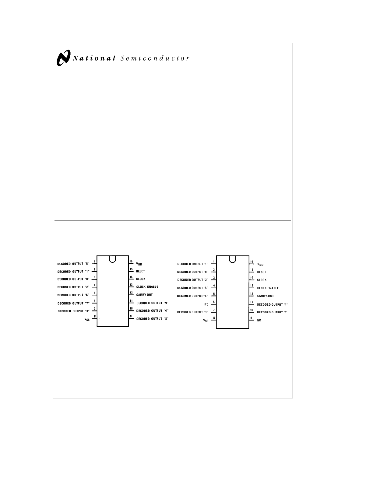
Connection Diagrams
CD4017B
Dual-In-Line Package
Features
Y
Wide supply voltage range 3.0V to 15V
Y
High noise immunity 0.45 VDD(typ.)
Y
Low power Fan out of 2 driving 74L
TTL compatibility or 1 driving 74LS
Y
Medium speed operation 5.0 MHz (typ.)
Y
Low power 10 mW (typ.)
Y
Fully static operation
with 10V V
Applications
Y
Automotive
Y
Instrumentation
Y
Medical electronics
Y
Alarm systems
Y
Industrial electronics
Y
Remote metering
CD4022B
Dual-In-Line Package
DD
Top View
C
1995 National Semiconductor Corporation RRD-B30M105/Printed in U. S. A.
TL/F/5950
TL/F/5950– 1
Top View
Order Number CD4017B or CD4022B
TL/F/5950– 2
Page 2
Absolute Maximum Ratings (Notes1&2)
If Military/Aerospace specified devices are required,
please contact the National Semiconductor Sales
Office/Distributors for availability and specifications.
DC Supply Voltage (V
DD
)
Input Voltage (VIN)
Storage Temperature (TS)
Power Dissipation (P
Dual-In-Line 700 mW
)
D
b
0.5 VDCtoa18 V
b
0.5 VDCto V
a
0.5 V
DD
b
65§Ctoa150§C
DC
DC
Recommended Operating
Conditions
DC Supply Voltage (VDD)
Input Voltage (VIN) 0 to VDDV
Operating Temperature Range (TA)
CD4017BM, CD4022BM
CD4017BC, CD4022BC
(Note 2)
a
3VDCtoa15 V
b
55§Ctoa125§C
b
40§Ctoa85§C
Small Outline 500 mW
Lead Temperature (T
(Soldering, 10 seconds) 260
)
L
C
§
DC Electrical Characteristics CD4017BM, CD4022BM (Note 2)
Symbol Parameter Conditions
I
DD
V
V
V
V
I
OL
I
OH
I
IN
Quiescent Device V
Current V
Low Level
OL
Output Voltage V
High Level
OH
Output Voltage V
Low Level
IL
Input Voltage V
High Level
IH
Input Voltage V
Low Level Output V
Current (Note 3) V
High Level Output V
Current (Note 3) V
Input Current V
e
DD
e
DD
e
V
DD
k
I
l
l
O
e
DD
e
V
DD
e
V
DD
k
I
l
l
O
e
DD
e
V
DD
e
V
DD
k
I
l
l
O
e
DD
e
V
DD
e
V
DD
k
I
l
l
O
e
DD
e
V
DD
e
V
DD
e
DD
e
DD
e
V
DD
e
DD
e
DD
e
V
DD
e
DD
e
V
DD
e
5V, V
10V, V
15V, V
1.0 mA
5V 0.05 0 0.05 0.05 V
10V 0.05 0 0.05 0.05 V
15V 0.05 0 0.05 0.05 V
1.0 mA
5V 4.95 4.95 5 4.95 V
10V 9.95 9.95 10 9.95 V
15V 14.95 14.95 15 14.95 V
1.0 mA
5V, V
10V, V
15V, V
1.0 mA
5V, V
10V, V
15V, V
5V, V
10V, V
15V, V
5V, V
10V, V
15V, V
15V, V
15V, V
VDDor V
IN
e
IN
e
IN
e
0.5V or 4.5V 1.5 1.5 1.5 V
O
e
1.0V or 9.0V 3.0 3.0 3.0 V
O
e
1.5V or 13.5V 4.0 4.0 4.0 V
O
e
0.5V or 4.5V 3.5 3.5 3.5 V
O
e
1.0V or 9.0V 7.0 7.0 7.0 V
O
e
1.5V or 13.5V 11.0 11.0 11.0 V
O
e
0.4V 0.64 0.51 0.88 0.36 mA
O
e
0.5V 1.6 1.3 2.25 0.9 mA
O
e
1.5V 4.2 3.4 8.8 2.4 mA
O
e
4.6V
O
e
9.5V
O
e
13.5V
O
e
IN
e
IN
b
55§C
Min Max Min Typ Max Min Max
SS
VDDor V
SS
VDDor V
SS
b
b
b
0V
15V 0.1 10
5 0.3 5 150 m A
10 0.5 10 300 m A
20 1.0 20 600 m A
0.25
0.62
1.8
b
0.1
b
0.2b0.36
b
0.5b0.9
b
1.5b3.5
a
25
§
b
5
b
b
10
b
5
0.1 1.0 mA
b
0.14 mA
b
0.35 mA
b
1.1 mA
0.1
a
125§C
b
1.0 mA
DC Electrical Characteristics CD4017BC, CD4022BC (Note 2)
b
Symbol Parameter Conditions
I
DD
V
OL
V
OH
Note 1: ‘‘Absolute Maximum Ratings’’ are those values beyond which the safety of the device cannot be guaranteed, they are not meant to imply that the devices
should be operated at these limits. The table of ‘‘Recommended Operating Conditions’’ and ‘‘Electrical Characteristics’’ provides conditions for actual device
operation.
Note 2: V
Note 3: I
Quiescent Device V
Current V
Low Level
Output Voltage V
High Level
Output Voltage V
e
0V unless otherwise specified.
SS
and IOHare tested one output at a time.
OL
e
5V 20 0.5 20 150 mA
DD
e
10V 40 1.0 40 300 mA
DD
e
15V 80 5.0 80 600 mA
V
DD
k
I
1.0 mA
l
l
O
e
5V 0.05 0 0.05 0.05 V
DD
e
V
10V 0.05 0 0.05 0.05 V
DD
e
15V 0.05 0 0.05 0.05 V
V
DD
k
I
1.0 mA
l
l
O
e
5V 4.95 4.95 5 4.95 V
DD
e
10V 9.95 9.95 10 9.95 V
V
DD
e
15V 14.95 14.95 15 14.95 V
V
DD
40§C
Min Max Min Typ Max Min Max
2
a
25
§
a
85§C
DC
DC
Units
Units
Page 3
DC Electrical Characteristics CD4017BC, CD4022BC (Note 2) (Continued)
b
Symbol Parameter Conditions
V
V
I
OL
I
OH
I
IN
Low Level
IL
Input Voltage V
High Level
IH
Input Voltage V
Low Level Output V
Current (Note 3) V
High Level Output V
Current (Note 3) V
Input Current V
Note 1: ‘‘Absolute Maximum Ratings’’ are those values beyond which the safety of the device cannot be guaranteed, they are not meant to imply that the devices
should be operated at these limits. The table of ‘‘Recommended Operating Conditions’’ and ‘‘Electrical Characteristics’’ provides condtions for actual device
operation.
Note 2: V
Note 3: I
e
0V unless otherwise specified.
SS
and IOHare tested one output at a time.
OL
k
I
1.0 mA
l
l
O
e
DD
e
V
DD
e
V
DD
k
I
l
l
O
e
DD
e
V
DD
e
V
DD
e
DD
e
DD
e
V
DD
e
DD
e
DD
e
V
DD
e
DD
e
V
DD
5V, V
10V, V
15V, V
1.0 mA
5V, V
10V, V
15V, V
5V, V
10V, V
15V, V
5V, V
10V, V
15V, V
15V, V
15V, V
e
0.5V or 4.5V 1.5 1.5 1.5 V
O
e
1.0V or 9.0V 3.0 3.0 3.0 V
O
e
1.5V or 13.5V 4.0 4.0 4.0 V
O
e
0.5V or 4.5V 3.5 3.5 3.5 V
O
e
1.0V or 9.0V 7.0 7.0 7.0 V
O
e
1.5V or 13.5V 11.0 11.0 11.0 V
O
e
0.4V 0.52 0.44 0.88 0.36 mA
O
e
0.5V 1.3 1.1 2.25 0.9 mA
O
e
1.5V 3.6 3.0 8.8 2.4 mA
O
e
4.6V
O
e
9.5V
O
e
13.5V
O
e
0V
IN
e
15V 0.3 10
IN
40§C
Min Max Min Typ Max Min Max
b
0.2
b
0.5
b
1.4
b
0.3
b
0.16b0.36
b
0.4b0.9
b
1.2b3.5
b
a
25
§
b
5
b
10
b
5
0.3 1.0 mA
b
0.12 mA
b
0.3 mA
b
1.0 mA
0.3
a
85§C
b
1.0 mA
AC Electrical Characteristics*
e
T
25§C, C
A
Symbol Parameter Conditions Min Typ Max Units
CLOCK OPERATION
t
PHL,tPLH
t
TLH,tTHL
f
CL
tWL,t
WH
t
rCL,tfCL
t
SU
C
IN
e
50 pF, R
L
Propagation Delay Time
Carry Out Line V
Carry Out Line V
Decode Out Lines V
Transition Time Carry Out
and Decode Out Lines
t
TLH
t
THL
Maximum Clock Frequency V
Minimum Clock V
Pulse Width V
Clock Rise and V
Fall Time V
Minimum Clock Inhibit V
Data Setup Time V
e
200k, t
L
rCL
and t
e
20 ns, unless otherwise specified
fCL
e
5V 415 800 ns
DD
e
10V 160 320 ns
V
DD
e
15V 130 250 ns
V
DD
e
5V 240 480 ns
DD
e
10V C
V
DD
e
15V ( 70 140 ns
V
DD
e
5V 500 1000 ns
DD
e
V
10V 200 400 ns
DD
e
15V 160 320 ns
V
DD
e
V
5V 200 360 ns
DD
e
10V 100 180 ns
V
DD
e
15V 80 130 ns
V
DD
e
V
5V 100 200 ns
DD
e
V
10V 50 100 ns
DD
e
15V 40 80 ns
V
DD
e
5V Measured with 1.0 2 MHz
DD
e
10V Respect to Carry 2.5 5 MHz
V
DD
e
15V (Output Line 3.0 6 MHz
V
DD
e
5V 125 250 ns
DD
e
10V 45 90 ns
DD
e
15V 35 70 ns
V
DD
e
5V 20 ms
DD
e
10V 15 ms
DD
e
15V 5 ms
V
DD
e
5V 120 240 ns
DD
e
10V 40 80 ns
DD
e
15V 32 65 ns
V
DD
e
15 pF 85 170 ns
L
Average Input Capacitance 5 7.5 pF
Units
3
Page 4

AC Electrical Characteristics*
e
T
A
Symbol Parameter Conditions Min Typ Max Units
RESET OPERATION
t
PHL, tPLH
t
W
t
REM
*AC Parameters are guaranteed by DC correlated testing.
25§C, C
e
50 pF, R
L
Propagation Delay Time
Carry Out Line V
e
200k, t
L
rCL
Carry Out Line V
Decode Out Lines V
Minimum Reset V
Pulse Width V
Minimum Reset V
Removal Time V
and t
e
20 ns, unless otherwise specified
fCL
e
5V 415 800 ns
DD
e
10V 160 320 ns
V
DD
e
15V 130 250 ns
V
DD
e
5V 240 480 ns
DD
e
10V C
V
DD
e
15V ( 70 140 ns
V
DD
e
5V 500 1000 ns
DD
e
V
10V 200 400 ns
DD
e
15V 160 320 ns
V
DD
e
5V 200 400 ns
DD
e
10V 70 140 ns
DD
e
15V 55 110 ns
V
DD
e
5V 75 150 ns
DD
e
10V 30 60 ns
DD
e
15V 25 50 ns
V
DD
e
15 pF 85 170 ns
L
Timing Diagrams
CD4017B
TL/F/5950– 3
4
Page 5

Timing Diagrams (Continued)
CD4022B
TL/F/5950– 4
5
Page 6

Logic Diagrams
CD4017B
Terminal No. 8eGND
Terminal No. 16eV
Terminal No. 16eV
Terminal No. 8eGND
DD
TL/F/5950– 5
CD4022B
DD
TL/F/5950– 6
6
Page 7

Physical Dimensions inches (millimeters)
Order Number CD4017BMJ, CD4017BCJ, CD4022BMJ, CD4022BCJ
Ceramic Dual-In-Line Package (J)
NS Package Number J16A
7
Page 8

Physical Dimensions inches (millimeters) (Continued)
Order Number CD4017BMN, CD4017BCN, CD4022BMN, CD4022BCN
Molded Dual-In-Line Package (N)
NS Package Number N16E
LIFE SUPPORT POLICY
NATIONAL’S PRODUCTS ARE NOT AUTHORIZED FOR USE AS CRITICAL COMPONENTS IN LIFE SUPPORT
DEVICES OR SYSTEMS WITHOUT THE EXPRESS WRITTEN APPROVAL OF THE PRESIDENT OF NATIONAL
CD4017BM/CD4017BC Decade Counter/Divider with 10 Decoded Outputs
SEMICONDUCTOR CORPORATION. As used herein:
CD4022BM/CD4022BC Divide-by-8 Counter/Divider with 8 Decoded Outputs
1. Life support devices or systems are devices or 2. A critical component is any component of a life
systems which, (a) are intended for surgical implant support device or system whose failure to perform can
into the body, or (b) support or sustain life, and whose be reasonably expected to cause the failure of the life
failure to perform, when properly used in accordance support device or system, or to affect its safety or
with instructions for use provided in the labeling, can effectiveness.
be reasonably expected to result in a significant injury
to the user.
National Semiconductor National Semiconductor National Semiconductor National Semiconductor
Corporation Europe Hong Kong Ltd. Japan Ltd.
1111 West Bardin Road Fax: (
Arlington, TX 76017 Email: cnjwge@tevm2.nsc.com Ocean Centre, 5 Canton Rd. Fax: 81-043-299-2408
Tel: 1(800) 272-9959 Deutsch Tel: (
Fax: 1(800) 737-7018 English Tel: (
National does not assume any responsibility for use of any circuitry described, no circuit patent licenses are implied and National reserves the right at any time without notice to change said circuitry and specifications.
Fran3ais Tel: (
Italiano Tel: (
a
49) 0-180-530 85 86 13th Floor, Straight Block, Tel: 81-043-299-2309
a
49) 0-180-530 85 85 Tsimshatsui, Kowloon
a
49) 0-180-532 78 32 Hong Kong
a
49) 0-180-532 93 58 Tel: (852) 2737-1600
a
49) 0-180-534 16 80 Fax: (852) 2736-9960
 Loading...