

Page 1
CD4016BM/CD4016BC Quad Bilateral Switch
CD4016BM/CD4016BC Quad Bilateral Switch
August 1989
General Description
The CD4016BM/CD4016BC is a quad bilateral switch intended for the transmission or multiplexing of analog or digital signals. It is pin-for-pin compatible with CD4066BM/
CD4066BC.
Features
Y
Wide supply voltage range 3V to 15V
Y
Wide range of digital and analog switchingg7.5 V
Y
‘‘ON’’ resistance for 15V operation 400X (typ.)
Y
Matched ‘‘ON’’ resistance over 15V
signal input DR
Y
High degree of linearity 0.4% distortion (typ.)
Y
Extremely low ‘‘OFF’’ switch leakage 0.1 nA (typ.)
@
V
DD
ON
e
f
1 kHz, V
IS
b
e
V
10V, R
SS
@
V
DD
e
10X (typ.)
e
IS
e
L
b
V
SS
T
A
PEAK
5V
10 kX
e
e
25§C
p-p
10V
,
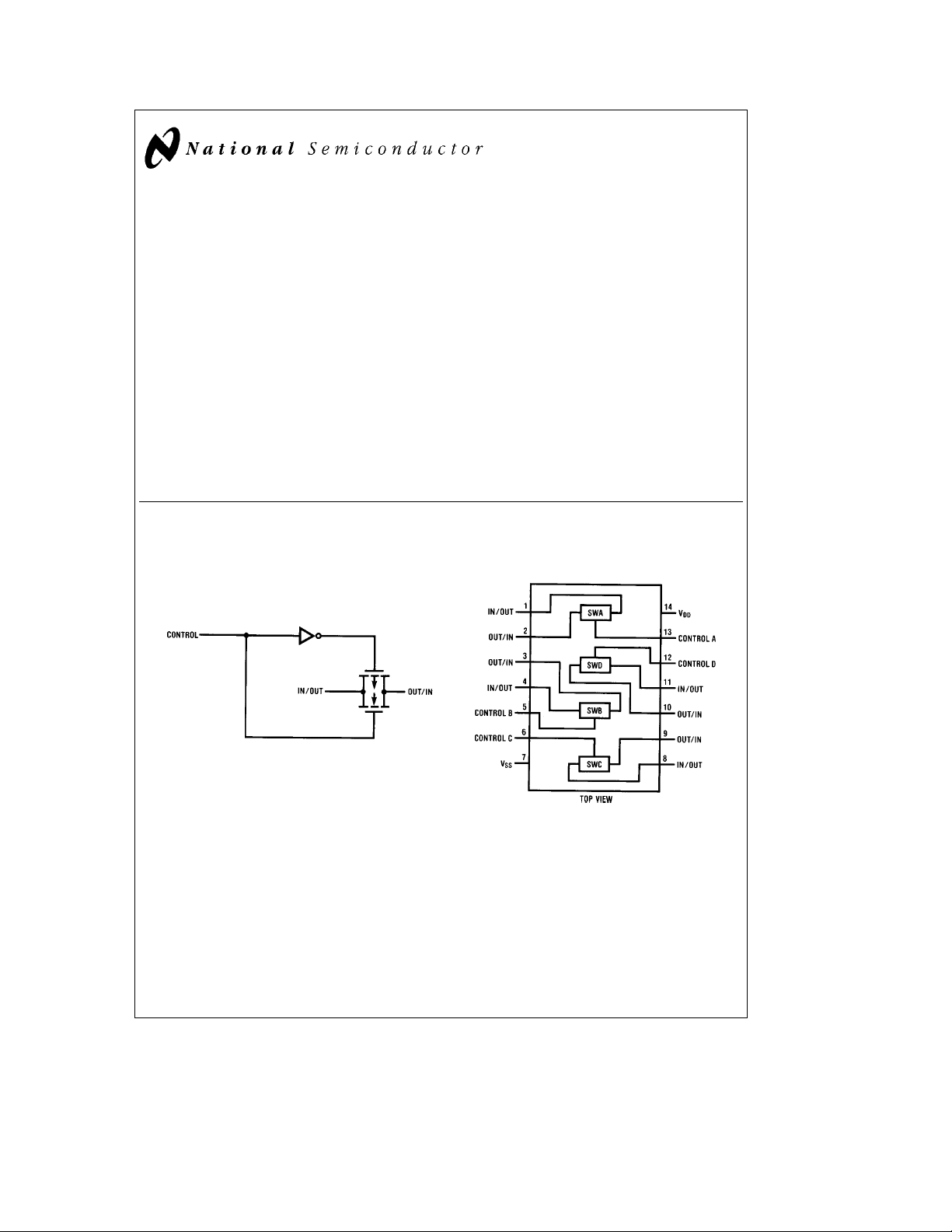
Schematic and Connection Diagrams
Y
Extremely high control input impedance 1012X (typ.)
Y
Low crosstalk between switches
Y
Frequency response, switch ‘‘ON’’ 40 MHz (typ.)
@
f
IS
e
0.9 MHz, R
b
50 dB (typ.)
L
Applications
Y
Analog signal switching/multiplexing
Signal gating
#
Squelch control
#
Chopper
#
Modulator/Demodulator
#
Commutating switch
#
Y
Digital signal switching/multiplexing
Y
CMOS logic implementation
Y
Analog-to-digital/digital-to-analog conversion
Y
Digital control of frequency, impedance, phase, and analog-signal gain
Dual-In-Line Package
e
1kX
Order Number CD4016B
TL/F/5661– 1
C
1995 National Semiconductor Corporation RRD-B30M105/Printed in U. S. A.
TL/F/5661
Page 2
Absolute Maximum Ratings
If Military/Aerospace specified devices are required,
please contact the National Semiconductor Sales
Office/Distributors for availability and specifications.
(Notes 1 and 2)
V
Supply Voltage
DD
Input Voltage
V
IN
TSStorage Temperature Range
b
0.5V toa18V
b
0.5V to V
b
65§Ctoa150§C
DD
a
0.5V
Power Dissipation (PD)
Dual-In-Line 700 mW
Small Outline 500 mW
Lead Temperature (Soldering, 10 seconds) 260
C
§
DC Electrical Characteristics CD4016BM (Note 2)
Symbol Parameter Conditions
I
DD
Quiescent Device Current V
Signal Inputs and Outputs
R
DR
‘‘ON’’ Resistance R
ON
D‘‘ON’’ Resistance R
ON
Between any 2 of
4 Switches
(In Same Package)
I
IS
Input or Output Leakage V
Switch ‘‘OFF’’ V
Control Inputs
V
V
I
IN
Low Level Input Voltage V
ILC
High Level Input Voltage V
IHC
Input Current V
e
DD
e
V
DD
e
V
DD
e
L
e
V
C
e
V
DD
e
V
DD
e
R
L
e
V
C
e
V
DD
e
V
DD
e
L
e
V
C
e
V
DD
e
V
DD
e
C
e
IS
e
V
OS
e
IS
e
V
OS
e
I
IS
e
V
DD
e
V
DD
e
V
DD
e
DD
e
V
DD
e
V
DD
b
DD
t
V
DD
t
V
DD
e
5V, V
VDDor V
IN
e
10V, V
IN
e
15V, V
IN
V
10 kX to
e
VDD,V
IS
10V 600 250 660 960 X
15V 360 200 400 600 X
V
10 kX to
V
DD
e
10V, V
IS
e
15V, V
IS
V
10 kX to
e
VDD,V
IS
10V 15 X
SS
VDDor V
SS
VDDor V
SS
b
V
DD
SS
2
VSSor V
DD
b
V
DD
SS
2
4.75 to 5.25V 1870 850 2000 2600 X
7.25 to 7.75V 775 400 850 1230 X
b
V
DD
SS
2
VSSto V
DD
15V 10 X
e
0, V
15V
DD
15V and 0V,
0V and 15V
VSSand V
g
VDDand V
10 mA
DD
SS
5V 0.9 0.7 0.5 V
10V 0.9 0.7 0.5 V
15V 0.9 0.7 0.5 V
5V 3.5 3.5 3.5 V
10V (see Note 6 and 7.0 7.0 7.0 V
15V
Figure 8
) 11.0 11.0 11.0 V
e
V
15V
SS
t
V
V
IS
SS
t
V
V
C
SS
Recommended Operating
Conditions
VDDSupply Voltage 3V to 15V
VINInput Voltage 0V to V
TAOperating Temperature Range
CD4016BM
CD4016BC
b
55§C25
Min Max Min Typ Max Min Max
g
(Note 2)
DD
b
55§Ctoa125§C
b
40§Ctoa85§C
C 125§C
§
Units
0.25 0.01 0.25 7.5 mA
0.5 0.01 0.5 15 mA
1.0 0.01 1.0 30 mA
g
50
0.1
g
0.1g50
b
g
10
g
500 nA
5
g
0.1
g
1.0 mA
2
Page 3
DC Electrical Characteristics CD4016BC (Note 2) (Continued)
b
Symbol Parameter Conditions
I
DD
Quiescent Device Current V
Signal Inputs and Outputs
R
DR
‘‘ON’’ Resistance R
ON
D‘‘ON’’ Resistance R
ON
Between any 2 of
4 Switches
(In Same Package) V
I
IS
Input or Output Leakage V
Switch ‘‘OFF’’ V
e
DD
e
V
DD
e
V
DD
e
L
e
V
C
e
V
DD
e
V
DD
e
R
L
e
V
C
e
V
DD
e
V
DD
e
L
e
V
C
e
V
DD
e
DD
e
C
e
IS
e
V
OS
e
5V, V
VDDor V
IN
e
10V, V
15V, V
10 kX to
VDD,V
10V 610 275 660 840 X
15V 370 200 400 520 X
10 kX to
V
DD
10V, V
15V, V
10 kX to
VDD,V
10V 15 X
VDDor V
IN
e
VDDor V
IN
b
V
DD
e
VSSor V
IS
b
V
DD
e
4.75 to 5.25V 1900 850 2000 2380 X
IS
e
7.25 to 7.75V 790 400 850 1080 X
IS
b
V
DD
e
VSSto V
IS
15V 10 X
e
0, V
15V
DD
0V or 15V,
15V or 0V
Control Inputs
V
V
I
IN
Low Level Input Voltage V
ILC
High Level Input Voltage V
IHC
Input Current V
e
VSSand V
IS
e
V
OS
e
g
I
IS
e
V
DD
e
V
DD
e
V
DD
e
DD
e
V
DD
e
V
DD
b
V
CC
t
V
V
DD
t
V
V
DD
DD
VDDand V
10 mA
SS
5V 0.9 0.7 0.4 V
10V 0.9 0.7 0.4 V
15V 0.9 0.7 0.4 V
5V 3.5 3.5 3.5 V
10V (see Note 6 and 7.0 7.0 7.0 V
15V
e
15V
SS
t
V
IS
SS
t
V
C
SS
V
SS
2
V
SS
2
V
SS
2
Figure 8
SS
SS
SS
DD
DD
40§C25
Min Max Min Typ Max Min Max
) 11.0 11.0 11.0 V
C85
§
C
§
1.0 0.01 1.0 7.5 mA
2.0 0.01 2.0 15 mA
4.0 0.01 4.0 30 mA
g
50
g
0.3
g
0.1g50
b
g
10
g
200 nA
5
g
0.3
g
1.0 mA
Units
AC Electrical Characteristics* T
A
25§C, t
r
e
t
20 ns and V
f
e
0V unless otherwise specified
SS
e
e
Symbol Parameter Conditions Min Typ Max Units
t
PHL,tPLH
t
PZH,tPZL
t
PHZ,tPLZ
Propagation Delay Time V
Signal Input to Signal Output R
Propagation Delay Time R
Control Input to Signal and3)
Output High Impedance to V
Logical Level V
Propagation Delay Time R
Control Input to Signal
Output Logical Level to V
High Impedance V
Sine Wave Distortion V
e
C
e
L
V
DD
V
DD
V
DD
e
L
DD
DD
V
DD
e
L
and3)
DD
DD
V
DD
e
C
e
R
L
e
VDD,C
200k
e
e
e
1.0 kX,C
e
e
e
1.0 kX,C
e
e
e
V
10 kX,V
(
Figure 4
50 pF, (
Figure 1
L
)
5V 58 100 ns
10V 27 50 ns
15V 20 40 ns
e
50 pF, (
L
Figures 2
5V 20 50 ns
10V 18 40 ns
15V 17 35 ns
e
50 pF, (
L
Figures 2
5V 15 40 ns
10V 11 25 ns
15V 10 22 ns
DD
e
5V, V
IS
)
eb
5 0.4 %
SS
e
5V
,fe1 kHz,
P-P
3
Page 4

AC Electrical Characteristics* (Continued)
e
T
A
Symbol Parameter Conditions Min Typ Max Units
C
IS
C
OS
C
IOS
C
IN
*AC Paramters are guaranteed by DC correlated testing.
Note 1: ‘‘Absolute Maximum Ratings’’ are those values beyond which the safety of the device cannot be guaranteed. They are not meant to imply that the devices
should be operated at these limits. The tables of ‘‘Recommended Operating Conditions’’ and ‘‘Electrical Characteristics’’ provide conditions for actual device
operation.
Note 2: V
Note 3: These devices should not be connected to circuits with the power ‘‘ON’’.
Note 4: In all cases, there is approximately 5 pF of probe and jig capacitance on the output; however, this capacitance is included in C
Note 5: V
Note 6: If the switch input is held at V
If the analog switch input is connected to V
maintain a V
e
25§C, t
t
r
e
20 ns and V
f
Frequency Response Ð Switch V
‘‘ON’’ (Frequency at
Feedthrough Ð Switch ‘‘OFF’’ V
(Frequency at
Crosstalk Between Any Two V
Switches (Frequency at
Crosstalk; Control Input to V
Signal Output R
Maximum Control Input R
e
0V unless otherwise specified
SS
b
3 dB) R
b
50 dB) R
b
50 dB) R
e
e
V
C
DD
e
1kX,V
L
20 Log
10VOS/VOS
Figure 4
)
(
e
5V, V
DD
e
1kX,V
L
20 Log10(VOS/VIS)eb50 dB,
Figure 4
)
(
e
V
DD
C(A)
e
1kXV
L
20 Log
10(VOS(B)/VOS(A)
Figure 5
)
(
e
10V, R
DD
e
1kX,V
IN
e
C
50 pF (
L
e
1kX,C
L
e
(/2 VOS(1 kHz)
V
OS(f)
e
5V 6.5 MHz
V
DD
e
10V 8.0 MHz
V
DD
e
15V 9.0 MHz
V
DD
eb
5V, V
e
IS
e
C
e
IS
e
5V; V
IS(A)
L
CC
Figure 6
e
L
5V, 40 MHz
SS
5V
,
P-P
(1 kHz)bdB,
eb
V
5V, 1.25 MHz
SS
5V
,
P-P
e
eb
V
SS
e
5V
,
P-P
e
10 kX 150 mV
e
10V Square Wave,
5V, 0.9 MHz
C(B)
)eb50 dB,
)
50 pF, (
Figure 7
)
Signal Input Capacitance 4 pF
Signal Output Capacitance V
Feedthrough Capacitance V
e
10V 4 pF
DD
e
0V 0.2 pF
C
Control Input Capacitance 5 7.5 pF
e
0V unless otherwise specified.
SS
is the voltage at the in/out pin and VOSis the voltage at the out/in pin. VCis the voltage at the control input.
IS
s
‘‘B’’ series. These currents are shown in
OL
is the control input level that will cause the switch output to meet the standard ‘‘B’’ series VOHand IOHoutput levels.
DD,VIHC
is the control input level Ð which allows the switch to
SS,VIHC
Figure 8
.
sink
standard ‘‘B’’ serieslI
L
, high level current, and still
l
OH
P-P
wherever it is specified.
AC Test Circuits and Switching Time Waveforms
Figure 1. t
FIGURE 2. t
PLH,tPLH
Propagation Delay Time Signal Input to Signal Output
PZH,tPHZ
Propagation Delay Time Control to Signal Output
4
TL/F/5661– 2
Page 5

AC Test Circuits and Switching Time Waveforms (Continued)
FIGURE 3. t
PZH,tPHZ
Propagation Delay Time Control to Signal Output
e
V
VDDfor distortion and frequency response tests
C
e
V
VSSfor feedthrough test
C
FIGURE 4. Sine Wave Distortion, Frequency Response and Feedthrough
FIGURE 5. Crosstalk Between Any Two Switches
FIGURE 6. Crosstalk Ð Control to Input Signal Output
5
TL/F/5661– 3
Page 6

AC Test Circuits and Switching Time Waveforms (Continued)
FIGURE 7. Maximum Control Input Frequency
Temperature Switch Input Switch Output
Range
V
DD
V
IS
T
LOW
IIS(mA)
25§CT
HIGH
V
OS
Min Max
5 0 0.25 0.2 0.14 0.4
MILITARY
55
b
0.25
10 0 0.62 0.5 0.35 0.5
10 10
b
0.62
b
0.2
b
0.5
b
0.14 4.6
b
0.35 9.5
15 0 1.8 1.5 1.1 1.5
15 15
b
1.8
b
1.5
b
1.1 13.5
5 0 0.2 0.16 0.12 0.4
COMMERCIAL
55
b
0.2
10 0 0.5 0.4 0.3 0.5
b
10 10
0.5
b
0.16
b
0.4
b
0.12 4.6
b
0.3 9.5
15 0 1.4 1.2 1.0 1.5
15 15
b
1.4
FIGURE 8. CD4016B Switch Test Conditions for V
b
1.2
b
1.0 13.5
IHC
Typical Performance Characteristics
‘ON’ Resistance vs. Signal
Voltage T
e
25§C
A
‘ON’ Resistance Temperature
Variation for V
DD
b
e
V
10V
SS
‘ON’ Resistance Temperature
Variation for V
DD
b
V
TL/F/5661– 4
(V)
e
15V
SS
TL/F/5661– 5
6
Page 7

Typical Applications
4 Input Multiplexer
Sample/Hold Amplifier
Special Considerations
The CD4016B is composed of 4, two-transistor analog
switches. These switches do not have any linearization or
compensation circuitry for ‘‘R
cause of this, the special operating considerations for
’’ as do the CD4066B’s. Be-
ON
the CD4066B do not apply to the CD4016B, but at low
TL/F/5661– 6
supply voltages,
s
5V, the CD4016B’s on resistance becomes non-linear. It is recommended that at 5V, voltages
on the in/out pins be maintained within about 1V of either
V
or VSS; and that at 3V the voltages on the in/out pins
DD
should be at V
or VSSfor reliable operation.
DD
7
Page 8

Physical Dimensions inches (millimeters)
Order Number CD4016CJ or CD4016MJ
CD4016BM/CD4016BC Quad Bilateral Switch
Dual-In-Line Package
NS Package J14A
Dual-In-Line Package
LIFE SUPPORT POLICY
Order Number CD4016CN
NS Package N14A
NATIONAL’S PRODUCTS ARE NOT AUTHORIZED FOR USE AS CRITICAL COMPONENTS IN LIFE SUPPORT
DEVICES OR SYSTEMS WITHOUT THE EXPRESS WRITTEN APPROVAL OF THE PRESIDENT OF NATIONAL
SEMICONDUCTOR CORPORATION. As used herein:
1. Life support devices or systems are devices or 2. A critical component is any component of a life
systems which, (a) are intended for surgical implant support device or system whose failure to perform can
into the body, or (b) support or sustain life, and whose be reasonably expected to cause the failure of the life
failure to perform, when properly used in accordance support device or system, or to affect its safety or
with instructions for use provided in the labeling, can effectiveness.
be reasonably expected to result in a significant injury
to the user.
National Semiconductor National Semiconductor National Semiconductor National Semiconductor
Corporation Europe Hong Kong Ltd. Japan Ltd.
1111 West Bardin Road Fax: (
Arlington, TX 76017 Email: cnjwge@tevm2.nsc.com Ocean Centre, 5 Canton Rd. Fax: 81-043-299-2408
Tel: 1(800) 272-9959 Deutsch Tel: (
Fax: 1(800) 737-7018 English Tel: (
National does not assume any responsibility for use of any circuitry described, no circuit patent licenses are implied and National reserves the right at any time without notice to change said circuitry and specifications.
Fran3ais Tel: (
Italiano Tel: (
a
49) 0-180-530 85 86 13th Floor, Straight Block, Tel: 81-043-299-2309
a
49) 0-180-530 85 85 Tsimshatsui, Kowloon
a
49) 0-180-532 78 32 Hong Kong
a
49) 0-180-532 93 58 Tel: (852) 2737-1600
a
49) 0-180-534 16 80 Fax: (852) 2736-9960
 Loading...