

Page 1
CD4002M/CD4002C Dual 4-Input NOR Gate
CD4012M/CD4012C Dual 4-Input NAND Gate
March 1988
CD4002M/CD4002C Dual 4-Input NOR Gate
CD4012M/CD4012C Dual 4-Input NAND Gate
General Description
These NOR and NAND gates are monolithic complementary MOS (CMOS) integrated circuits. The N- and P-channel
enhancement mode transistors provide a symmetrical circuit with output swings essentially equal to the supply voltage. This results in high noise immunity over a wide supply
voltage range. No DC power other than that caused by leakage current is consumed during static conditions. All inputs
are protected against static discharge and latching conditions.
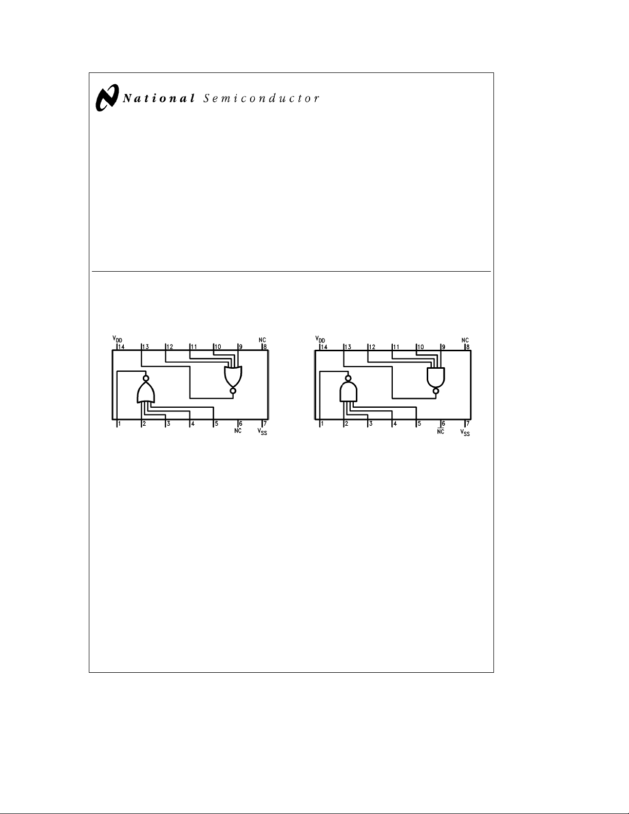
Connection Diagrams
CD4002
Dual-In-Line Package
TL/F/5940– 1
Top View
Order Number CD4002 or CD4012
Features
Y
Wide supply voltage range 3.0V to 15V
Y
Low power 10 nW (typ.)
Y
High noise immunity 0.45 VDD(typ.)
Applications
Y
Automotive
Y
Data terminals
Y
Instrumentation
Y
Medical Electronics
Dual-In-Line Package
Y
Y
Y
Y
CD4012
Top View
Alarm system
Industrial controls
Remote metering
Computers
TL/F/5940– 2
C
1995 National Semiconductor Corporation RRD-B30M105/Printed in U. S. A.
TL/F/5940
Page 2
Absolute Maximum Ratings (Note 1)
If Military/Aerospace specified devices are required,
please contact the National Semiconductor Sales
Office/Distributors for availability and specifications.
Voltage at Any Pin V
Operating Temperature Range
CD4002M, CD4012M
CD4002C, CD4012C
SS
b
0.3V to V
DD
b
55§Ctoa125§C
b
40§Ctoa85§C
a
0.3V
Storage Temperature Range (T
S
Power Dissipation (PD)
Dual-In-Line 700 mW
Small Outline 500 mW
Operating Range (V
)V
DD
Lead Temperature (TL)
(Soldering, 10 seconds) 260
b
)
SS
a
3.0V to V
65§Ctoa150§C
SS
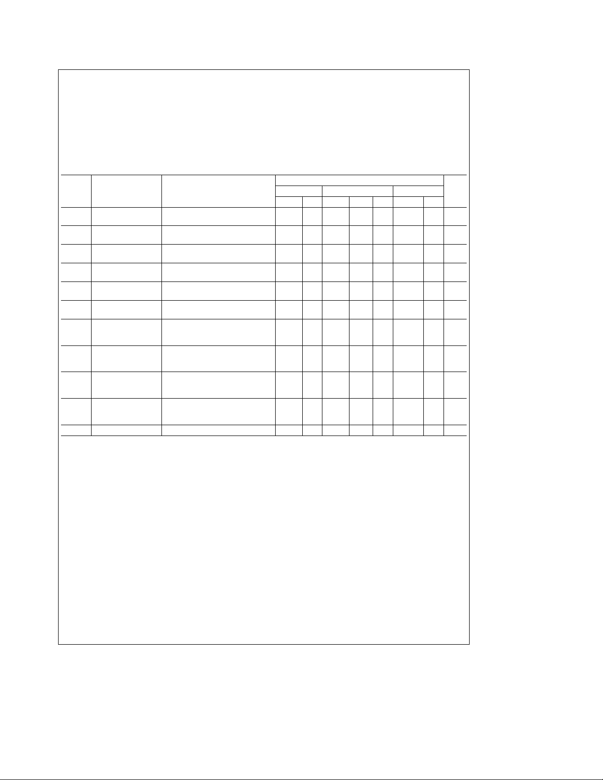
DC Electrical Characteristics CD4002M, CD4012M
Limits
Symbol Parameter Conditions
b
55§C
Min Max Min Typ Max Min Max
I
P
V
V
V
V
IDN Output Drive Current V
IDP Output Drive Current V
IDN Output Drive Current V
IDP Output Drive Current V
I
Quiescent V
DD
Device Current V
Quiescent Device V
D
Dissipation/Package V
Output Voltage V
OL
Low Level V
Output Voltage V
OH
High Level V
Noise Immunity V
NL
(All Inputs) V
Noise Immunity V
NH
(All Inputs) V
N-Channel (4002) V
(Note 2)
P-Channel (4002) V
(Note 2)
N-Channel (4012) V
(Note 2)
P-Channel (4012) V
(Note 2)
Input Current 10 pA
I
Note 1: ‘‘Absolute Maximum Ratings’’ are those values beyond which the safety of the device cannot be guaranteed. Except for ‘‘Operating Temperature Range’’
they are not meant to imply that the devices should be operated at these limits. The table of ‘‘Electrical Characteristics’’ provides conditions for actual device
operation.
Note 2: I
N and IDP are tested one output at a time.
D
e
5.0V 0.05 0.001 0.05 3.0 mA
DD
e
10V 0.1 0.001 0.1 6 mA
DD
e
5.0V 0.25 0.005 0.25 15 mW
DD
e
10V 1.0 0.01 1.0 60 mW
DD
DD
DD
DD
DD
DD
DD
DD
DD
DD
DD
DD
DD
DD
DD
DD
DD
e
e
e
e
e
e
e
e
e
e
e
e
e
e
e
e
5.0V, V
10V, V
5.0V, V
10V, V
5.0V, V
10V, V
5.0V, V
10V, V
5.0V, V
10V, V
5.0V, V
10V, V
5.0V, V
10V, V
5.0V, V
10V, V
e
I
e
I
e
I
e
I
e
O
e
O
e
O
e
O
e
O
e
O
e
O
e
O
e
O
e
O
e
O
e
O
VDD,I
VDD,I
VSS,I
VSS,I
3.6V, I
7.2V, I
0.95V, I
2.9V, I
0.4V, V
0.5V, V
2.5V, V
9.5V, V
0.4V, V
0.5V, V
2.5V, V
9.5V, V
e
0A 0.05 0 0.05 0.05 V
O
e
0A 0.05 0 0.05 0.05 V
O
e
0A 4.95 4.95 5.0 4.95 V
O
e
0A 9.95 9.95 10 9.95 V
O
e
0A 1.5 1.5 2.25 1.4 V
O
e
0A 3.0 3.0 4.5 2.9 V
O
e
0A 1.4 1.5 2.25 1.5 V
O
e
0A 2.9 3.0 4.5 3.0 V
O
e
V
I
e
I
e
I
e
I
e
I
e
I
e
I
e
I
0.5 0.40 1.0 0.28 mA
DD
V
1.1 0.9 2.5 0.65 mA
DD
b
V
0.62
SS
b
V
0.62
SS
VDD0.31 0.25 0.5 0.175 mA
V
0.63 0.5 0.6 0.35 mA
DD
b
V
0.31
SS
b
V
0.75
SS
a
b
0.5b2.0
b
0.5b1.0
b
0.25b0.5
b
0.6b1.2
25§C
a
125§C Units
b
0.35 mA
b
0.35 mA
b
0.175 mA
b
0.4 mA
a
15V
C
§
2
Page 3

DC Electrical Characteristics CD4002C, CD4012C
Limits
Symbol Parameter Conditions
b
55§C
Min Max Min Typ Max Min Max
I
P
V
V
V
V
IDN Output Drive Current V
IDN Output Drive Current V
IDP Output Drive Current V
IDP Output Drive Current V
I
Quiescent V
DD
Device Current V
Quiescent Device V
D
Dissipation/Package V
Output Voltage V
OL
Low Level V
Output Voltage V
OH
High Level V
Noise Immunity V
NL
(All Inputs) V
Noise Immunity V
NH
(All Inputs) V
N-Channel (4002) V
(Note 2)
N-Channel (4012) V
(Note 2)
P-Channel (4002) V
(Note 2)
P-Channel (4012) V
(Note 2)
Input Current 10 pA
I
Note 1: ‘‘Absolute Maximum Ratings’’ are those values beyond which the safety of the device cannot be guaranteed. Except for ‘‘Operating Temperature Range’’
they are not meant to imply that the devices should be operated at these limits. The table of ‘‘Electrical Characteristics’’ provides conditions for actual device
operation.
Note 2: I
N and IDP are tested one output at a time.
D
e
5.0V 0.5 0.005 0.5 15 mA
DD
e
10V 5.0 0.005 5.0 30 mA
DD
e
5.0V 2.5 0.025 2.5 75 mW
DD
e
10V 50 0.05 50 300 mW
DD
DD
DD
DD
DD
DD
DD
DD
DD
DD
DD
DD
DD
DD
DD
DD
DD
e
e
e
e
e
e
e
e
e
e
e
e
e
e
e
e
5.0V, V
10V, V
5.0V, V
10V, V
5.0V, V
10V, V
5.0V, V
10V, V
5.0V, V
10V, V
5.0V, V
10V, V
5.0V, V
10V, V
5.0V, V
10V, V
e
I
e
I
e
I
e
I
t
O
t
O
s
O
s
O
e
O
e
O
e
O
e
O
e
O
e
O
e
O
e
O
VDD,I
VDD,I
VSS,I
VSS,I
3.6V, I
7.2V, I
0.95V, I
2.9V, I
0.4V, V
0.5V, V
0.4V, V
0.5V, V
2.5V, V
9.5V, V
2.5V, V
9.5V, V
e
0A 0.05 0 0.05 0.05 V
O
e
0A 0.05 0 0.05 0.05 V
O
e
0A 4.95 4.95 5.0 4.95 V
O
e
0A 9.95 9.95 10 9.95 V
O
e
0A 1.5 1.5 2.25 1.4 V
O
e
0A 3.0 3.0 4.5 2.9 V
O
e
0A 1.4 1.5 2.25 1.5 V
O
e
0A 2.9 3.0 4.5 3.0 V
O
e
V
I
e
I
e
I
e
I
e
I
e
I
e
I
e
I
0.35 0.3 1.0 0.24 mA
DD
V
0.72 0.6 2.5 0.48 mA
DD
VDD0.145 0.12 0.5 0.095 mA
V
0.3 0.25 0.6 0.2 mA
DD
b
V
0.35
SS
b
V
V
V
0.3
SS
b
0.145
SS
b
0.35
SS
a
b
0.3b2.0
b
0.25b1.0
b
0.12b0.5
b
0.3b1.2
25§C
a
85§C Units
b
0.24 mA
b
0.2 mA
b
0.095 mA
b
0.24 mA
3
Page 4

AC Electrical Characteristics* T
temperature coefficient for all values of V
DD
e
0.3%/§C.
e
A
25§C, C
e
15 pF, and input rise and fall timese20 ns. Typical
L
Symbol Parameter Conditions Min Typ Max Units
CD4002M
t
t
t
t
C
PHL
PLH
THL
TLH
IN
Propagation Delay Time V
High to Low Level V
Propagation Delay Time V
Low to High Level V
Transition Time High V
to Low Level V
Transition Time Low V
to High Level V
Input Capacitance Any Input 5.0 pF
e
5.0V 35 50 ns
DD
e
10V 25 40 ns
DD
e
5.0V 35 50 ns
DD
e
10V 25 40 ns
DD
e
5.0V 65 175 ns
DD
e
10V 35 75 ns
DD
e
5.0V 65 125 ns
DD
e
10V 35 70 ns
DD
CD4002C
t
PHL
T
PLH
t
THL
t
TLH
C
IN
*AC Parameters are guaranteed by DC correlated testing.
Propagation Delay Time V
High to Low Level V
Propagation Delay Time V
Low to High Level V
Transition Time High V
to Low Level V
Transition Time Low V
to High Level V
Input Capacitance Any Input 5.0 pF
e
5.0V 35 120 ns
DD
e
10V 25 65 ns
DD
e
5.0V 35 80 ns
DD
e
10V 25 55 ns
DD
e
5.0V 65 300 ns
DD
e
10V 35 125 ns
DD
e
5.0V 65 200 ns
DD
e
10V 35 115 ns
DD
AC Electrical Characteristics* T
temperature coefficient for all values of V
DD
e
0.3%/§C.
e
A
25§C, C
e
15 pF, and input rise and fall timese20 ns. Typical
L
Symbol Parameter Conditions Min Typ Max Units
CD4012M
t
t
t
t
C
PHL
PLH
THL
TLH
IN
Propagation Delay Time V
High to Low Level V
Propagation Delay Time V
Low to High Level V
Transition Time High V
to Low Level V
Transition Time Low V
to High Level V
Input Capacitance Any Input 5.0 pF
e
5.0V 50 75 ns
DD
e
10V 25 40 ns
DD
e
5.0V 50 75 ns
DD
e
10V 25 40 ns
DD
e
5.0V 75 125 ns
DD
e
10V 50 75 ns
DD
e
5.0V 75 100 ns
DD
e
10V 40 60 ns
DD
CD4012C
t
PHL
T
PLH
t
THL
t
TLH
C
IN
*AC Parameters are guaranteed by DC correlated testing.
Note 1: ‘‘Absolute Maximum Ratings’’ are those values beyond which the safety of the device cannot be guaranteed. Except for ‘‘Operating Temperature
Range’’ they are not meant to imply that the devices should be operated at these limits. The table of ‘‘Electrical Characteristics’’ provides conditions for actual
device operation.
Propagation Delay Time V
High to Low Level V
Propagation Delay Time V
Low to High Level V
Transition Time High V
to Low Level V
Transition Time Low V
to High Level V
Input Capacitance Any Input 5.0 pF
e
5.0V 50 100 ns
DD
e
10V 25 50 ns
DD
e
5.0V 50 100 ns
DD
e
10V 25 50 ns
DD
e
5.0V 75 150 ns
DD
e
10V 50 100 ns
DD
e
5.0V 75 125 ns
DD
e
10V 40 75 ns
DD
4
Page 5

Physical Dimensions inches (millimeters)
Order Number CD4002MJ, CD4002CJ, CD4012MJ or CD4012CJ
Ceramic Dual-In-Line Package (J)
NS Package Number J14A
5
Page 6

Physical Dimensions inches (millimeters) (Continued)
Order Number CD4002MN, CD4002CN, CD4012MN or CD4012CN
Molded Dual-In-Line Package (N)
NS Package Number N14A
CD4002M/CD4002C Dual 4-Input NOR Gate
CD4012M/CD4012C Dual 4-Input NAND Gate
LIFE SUPPORT POLICY
NATIONAL’S PRODUCTS ARE NOT AUTHORIZED FOR USE AS CRITICAL COMPONENTS IN LIFE SUPPORT
DEVICES OR SYSTEMS WITHOUT THE EXPRESS WRITTEN APPROVAL OF THE PRESIDENT OF NATIONAL
SEMICONDUCTOR CORPORATION. As used herein:
1. Life support devices or systems are devices or 2. A critical component is any component of a life
systems which, (a) are intended for surgical implant support device or system whose failure to perform can
into the body, or (b) support or sustain life, and whose be reasonably expected to cause the failure of the life
failure to perform, when properly used in accordance support device or system, or to affect its safety or
with instructions for use provided in the labeling, can effectiveness.
be reasonably expected to result in a significant injury
to the user.
National Semiconductor National Semiconductor National Semiconductor National Semiconductor
Corporation Europe Hong Kong Ltd. Japan Ltd.
1111 West Bardin Road Fax: (
Arlington, TX 76017 Email: cnjwge@tevm2.nsc.com Ocean Centre, 5 Canton Rd. Fax: 81-043-299-2408
Tel: 1(800) 272-9959 Deutsch Tel: (
Fax: 1(800) 737-7018 English Tel: (
National does not assume any responsibility for use of any circuitry described, no circuit patent licenses are implied and National reserves the right at any time without notice to change said circuitry and specifications.
Fran3ais Tel: (
Italiano Tel: (
a
49) 0-180-530 85 86 13th Floor, Straight Block, Tel: 81-043-299-2309
a
49) 0-180-530 85 85 Tsimshatsui, Kowloon
a
49) 0-180-532 78 32 Hong Kong
a
49) 0-180-532 93 58 Tel: (852) 2737-1600
a
49) 0-180-534 16 80 Fax: (852) 2736-9960
 Loading...