

Page 1
National Semiconductor
July 25, 2006
Rev - 2.1/CS
RoHS Compliant
Evaluation Board User's Guide
ADC121S625 12-Bit, 50 kSPS to 200 kSPS, Differential
Input, Micro-Power Sampling A/D Converter
1 http://www.national.com
Page 2

Table of Contents
1.0 Introduction 3
2.0 Board Assembly 3
3.0 Quick Start 4
3.1 Stand Alone Mode 4
3.2 Computer Mode 4
4.0 Functional Description 5
4.1 The Signal Input 5
4.2 ADC Reference Circuitry 5
4.3 ADC Clock Circuit 5
4.4 Digital Data Output 5
4.5 Power Supply Connections 5
5.0 Software Operation and Settin gs 6
6.0 Hardware Schematic 7
7.0 Evaluation Board Specifications 8
8.0 ADC121S625B Evaluat ion Bo ard Bi ll of Materials 8
9.0 Tables of Test Points, Jumpers and Connectors 9
2 http://www.national.com
Page 3
1.0 Introduction
The ADC121S625EVAL/RoHS Design Kit
(consisting of the ADC121S625B Evaluation
Board and this User's G uide) is designed to ease
evaluation and design-in of the National
Semiconductor ADC121S625 12-bit Analog-toDigital Converter, whic h ca n operate at speeds up
to 200 kSPS.
The evaluation boar d can be used in either of t wo
modes. In the Stand-Alone or Manual mode,
suitable test eq uipment, such as a logic analyzer ,
can be used with the board to evaluate the
ADC121S625’s performance.
In the Computer or Automatic mode, data capture
and evaluation is simplified by connecting this
board to National Semiconductor's Data Capture
Board (order number WAVEVSN BRD 4.0) with a
ribbon cable (order number WV4ADCIFCABLE),
which is connected to a personal computer
through a USB port and running WaveVision4
software. The WaveVision4 program can be
downloaded from the web at
http://www.national.com/adc
.
VREF
select
The WaveVision4 software operates under
Microsoft Windows. The signal at the Ana lo g In put
is digitized, captured, and displayed on a PC
monitor in the time and frequency domain.
The software will perform an FFT on the captured
data upon command. This FFT plot shows
dynamic perform ance in the form of SNR, SIN AD,
THD, SFDR and ENOB. A histogram of the
captured data is also available.
The differential si gnal at analog inp uts J2 or J3 is
digitized by U1, the ADC121S625.
The ADC121S625 uses an external oscillator that
is provided on this board by Y2 or J6.
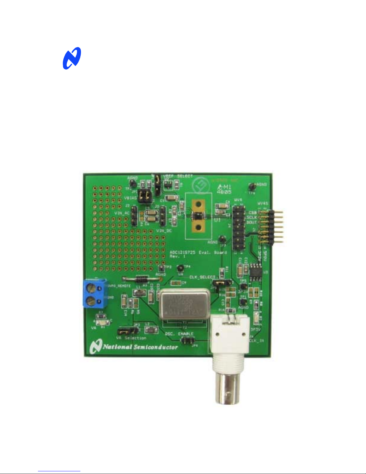
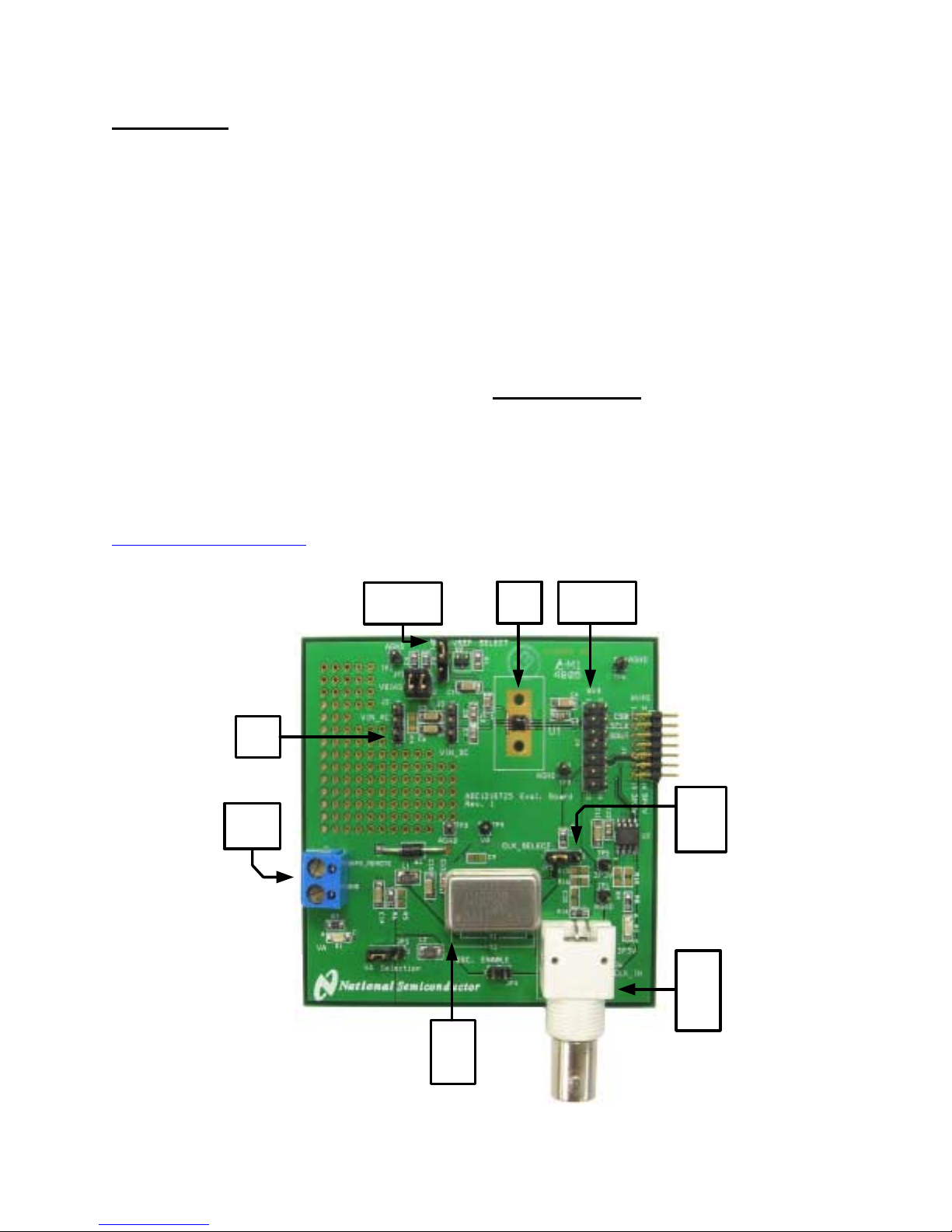
2.0 Board Assembly
The ADC121S625B e valuation board comes fully
assembled and read y for use. Refer to the Bill of
Materials for a description of components, to
Figure 1 for major component placement and to
Figure 2 for the Evaluation Board schematic.
U1
DUT
WV4
connector
J2
VIN
JP5
5V
remote
CLK
select
J6
EXT
CLK
input
Y2
CLK
OSC
3 http://www.national.com
Page 4

Figure 1 Component and Test Point Locations
3.0 Quick Start
The ADC121S625B evaluation board may be
used in the Stand-Alone mode to capture data
with a logic analyzer or third par ty equipm ent, or it
may be used in the Computer Mode with a
WaveVision4 Data C apture (WV4) Board. In both
cases, the data may be analyzed with the
WaveVision4 software.
3.1 Stand Alone Mode
Refer to Figure 1 for locations of test points and
major components.
1. Install an appropriate crystal oscillator into
socket Y2 and short pins 1 & 2 of JP5 (See
Table 1). Alternatively, connect a signal
generator with TTL logic levels to BNC
connector J6 and short pins 2 & 3 of JP5. I n
either case, short pins 4 & 10 of J4 to pro vide
the clock signal to the AD C121S625. If using
an external source, rem ove the os cillator f rom
Y2. If using an oscillator at Y2, remove the
signal source from J6. The presence of a
second clock source could add noise to the
conversion process.
2. Connect a clean analog (non-switching) +5V
power source to Power Connector J5.
3. Short pins 1 & 2 of JP3 an d turn on the power
supply.
4. Dynamic differential signal sources centered
around ground should be connected across
pins 1 & 3 of J2. Pin 2 of J2 is gr ound. If the
source has a 50Ω output im pedance, install a
51 ohm resistor at R4. Otherwise, the signal
level will be twice as large as expected. To
accurately evaluate the performance of the
ADC121S625, the sourc e must be better than
90dB THD.
5. Short pins 1 & 2 and pins 3 & 4 of JP2 to
provide the bias volta ge of VREF for the in put
to the ADC when driving the ADC from J2.
6. Differential DC sources or dynam ic diff erential
signal sources centered at a DC bias point
should be connected acr oss pins 1 & 3 of J3.
Pin 2 of J3 is ground.
7. Remove the shorts ac ros s pins 1 & 2 and pi ns
3 & 4 of JP2 wh en driving the ADC input from
J3.
8. Select the 2.5V shunt voltage reference as
VREF by shorting pins 2 & 3 of JP1 or select
VA as VREF by shorting pins 1 & 2 of JP1. If it
is desirable to provide an external reference
voltage, the jumper must be removed from
JP1 and pin 2 may be driven directly.
9. The digital inp uts and out p uts are av ai la ble f or
probing at J4.
3.2 Computer Mode
Refer to Figure 1 for locations of test points and
major components.
1. Run the WaveVision4 program. Version 4.2
or higher is required to interface the WV4
board with the ADC121S625B evaluation
board. While the program is loading, c ontinu e
below.
2. Install an appropriate crystal oscillator into
socket Y2 and short pins 1 & 2 of JP5 (See
Table 1). Alternatively, connect a signal
generator with TTL logic levels to BNC
connector J6 and short pins 2 & 3 of JP5.
3. Connect a USB cable between the
WaveVision4 Data Capture Board a nd the P C
running the WaveVision4 program.
4. Connect a ribbon cable (order number
WV4ADCIFCABLE) between J4 of the
ADC121S625B evaluation boar d and J3 of the
WV4 board.
5. Connect a clean analog (non-switching) +5V
power source to Power Connector J5.
6. Short pins 1 & 2 of JP3 an d turn on the power
supply. See Section 4.5 for detailed Power
Supply Information
7. Connect a separate an alog +5V p ower sour ce
to power connector J1 on the W V4 board and
turn on the power.
8. Connect a jumper cable between TP10
(+3.3V) of the W V4 board and TP5 (3P3V) of
the ADC121S625B board.
9. Perform steps 4 & 5 or 6 & 7 of section 3.1 t o
drive the analog inputs.
10. Perform step 8 of section 3.1 to select the
reference voltage.
11. Refer to section 5.0 on Software Operation
and Settings.
4 http://www.national.com
Page 5

4.0 Functional Description
Table 1 describes the function of the various
jumpers on the ADC121S625B evaluation board.
The Evaluation Board schematic is shown in
Figure 2.
Jumper Pins 1 & 2 Pins 2 & 3
JP1
JP2
JP3
Select VA as the
VREF
Short pins 1 & 2 and pins 3 & 4 to
bias input pins at VREF
Select
5P0V_REMOTE
from J5
Select 2.5V reg.
as the VREF
Select 5P0V from
J1 (WV4S)
JP4 Enable OSC (not required)
JP5
Select on-board
clock OSC Y2
Select clock OSC
at BNC J6
Table 1 Jumper Functions
4.1 The Signal Input
The input signal t o be digitized sh ould be applied
across pins 1 & 3 of J2 or J3.
For input signals centered around ground, J2
should be utilized. Pin 2 of J 2 is ground. Resistor
R4 is a terminating resistor for the input source.
Since all sources do not have the same output
impedance, R4 is not stuffed. However, it is
recommended that it is stuffed by the end user
with the appropriate value that matches the
source.
The DC biasing for inpu ts a ppl ied to J 2 is s up pl ied
through JP2. Short pins 1 & 2 and 3 & 4 of JP2 to
properly bias the input to VREF.
If it is desired to digitize a differential DC voltage
or a dynamic signa l th at is alrea d y pr op erl y bias ed
for the ADC121S625, apply the signal to be
digitized across pins 1 & 3 of J3. Pin 2 of J3 is
ground. When applying the inp ut at J3, all shorts
on JP2 need to be removed.
Dynamic input s ignals should be applied through
a bandpass filter to eliminate the noise and
harmonics commonly associated with signal
sources. To accur ately evaluate the perfor mance
of the ADC121S625, the source must be better
than 90dB THD
4.2 ADC Reference Circuitry
This evaluation board includes the option of
selecting a fixed 2.5 V shunt voltage reference or
VA as the reference voltage. Select the 2.5V
reference as VREF b y shorting pins 2 & 3 of JP1
or select VA as VREF by shorting pins 1 & 2 of
JP1. If it is desirable to provide an external
reference voltage, the jumper must be removed
from JP1 and pin 2 may be driven directly.
If it is desirable t o cha nge t he LM40 40DIM3- 2.5 to
an LM4040 with a different voltage, carefully
remove it and adjust the value of R3 to limit the
current through the LM4040.
4.3 ADC Clock Circuit
The crystal-based oscillator provided on the
evaluation board is selected by shorting pins 1 & 2
of JP5. It is best to remove any external signal
generator from J6 when using this oscillator to
reduce any unnecessar y noise.
This board will als o accept a clock s ignal from an
external source by connec ting that source to BNC
J6 and shorting pins 2 & 3 of JP5. The input
applied at J6 is 50 ohm terminated by R14. The
external clock signal must meet TTL input
requirements. It is best to remove the oscillator at
Y2 when using an externa l clock sourc e to reduce
any unnecessary noise.
Regardless of the clock source selected by JP5,
the clock signal is designed to be routed off the
ADC121S625B evaluation board to National’s
WV4 board. This assumes a “computer mode”
operation of the e va luatio n board. F or a ppl ic at ions
utilizing the evaluation board in manual mode,
short pins 4 & 10 of J 4 with a short j umper wire to
provide the clock signal to the ADC121S625.
4.4 Digital Data Output
The serial data output from this board may be
monitored at J1 or J4.
4.5 Power Supply Connections
When operating in “com puter m ode” with t he W V4
Board, voltage 5P0V for VA and 3P3V for U3
must be supplied to the AD C121 S6 25B e va lua tio n
board. For best performance from the
ADC121S625, the 5P 0V voltag e for VA should be
supplied by a separate power supply to J5. The
3P3V voltage may be pulled off the WV4 Board
with a jumper wire at TP10 (W V4) and applied to
TP5.
When operating in “manual mode”, only voltage
5P0V needs to be applied to J5.
The 5P0V voltage nee ds to be s et between +4.5V
and +5.5V and a shorting j umper must be placed
across pins 1 & 2 of JP3.
5.0 Software Operation and Settings
5 http://www.national.com
Page 6

The WaveVision4 software is included with the
WV4 board and the latest version can be
downloaded for free from National's web site at
http://www.national.com/adc
. To install this
software, follow the proced ure in the WaveVision4
Board User's Guide. Once the software is
installed, run it and set it up as follows:
1. Connect the WV4 board to the host computer
with a USB cable.
2. From the WaveVision main menu, go to
Settings, then Board Settings and do the
following:
Select the following from the WaveVision4
main menu:
• WaveVision 4.0 (USB)
• # of Samples: 2K to 32K, as desired
3. Apply power as specif ied in Section 4.5, click
on the "Test" button and await the firmware
to download.
4. Click on the "Accept" button.
5. After the steps outlined in Section 3.2 are
completed, click on ‘A
cquire’ then ‘Samples’
from the Main Menu (you can als o press the
F1 shortcut key). If a di alog box ope ns, select
‘D
iscard’ or press the Escape key to start
collecting new updated samples.
A plot of the selected num ber of samples will be
displayed. Make s ure there is no clipping of data
samples. The samples may be further analyzed
by clicking on the magnifying glass icon, then
clicking and draggi ng ac ross a specif ic ar ea of the
plot for better data inspection. See the
WaveVision4 Board User's Guide for details.
To view an FFT of the data captured, click on the
‘FFT’ tab. This plot may be zoomed in on lik e the
data plot. A display of dynamic performance
parameters in the form of SINAD, SNR, THD,
SFDR and ENOB will be di spla yed at the top right
hand corner of the FFT plot.
Acquired data m ay be saved to a fil e. Plots may
also be exported as graphics. See the Data
Capture Board User's Guide for details.
6 http://www.national.com
Page 7

6.0 Hardware Schematic
3P3V
3P3V
1
TP5
3P3V
U3
24C02
5
SCL
6
WP
SCL
WV4S
2468101214
J1
WV4S
13579
CSB
SCLK
1.0uF
0.1uF
U1
ADC121S625C IMT
0.1uF
0.1uF
1.0uF
3
1
JP2
DOUT
SCLK
DOUT
CSB
7
6
8
VA
SCLK
VREF1+IN2-IN3GND
4
2
HEADER 2X2
C5 1.0uF
R4
NS
123
J2
VIN_AC
DOUT
AGND
1
TP1
AGND
VA
C4
C3
R1 2K
U2
LM4040/SOT23
3
2
1
JP1
VREF SELECT
VA
2 1
C2A
C2B
C1
R2
5.1K
R3
5.1K
VREF
TP2
AGND
VBIAS
AGND
1
5P0V
11
13
3P3V
SDA
CLKSEND
5
AGND
CSB
1
TP3
AGND
4
C8
470pF
C7
470pF
3
2
1
J3
VIN_DC
VIN_DC
C6 1.0uF
VIN_AC
5P0V
3P3V
WV4
13579
J4
WV4
246
CSB
SCLK
Perforated Board A r ea
SCL
1112
1314
8
10
DOUT
SDA
CLKSEND
CLKSEND
L1
100uH
100 mil inch spacing
37 mil inch drills with 57 mil inch pads
7
VCC
8
C12
0.1uF
3P3V
C11
1.0uF
5P5V
R6
0
R5
C10
C9
TP4
VA
VA
NS
3P3V
3P3V
1.0uF
Y1
4.0MHz OSC
1
OE
VDD4GND
2
OUT
3
NS
C13
L2
100uH
5P0V
VA
C14
1.0uF
R7
1
VA
510
VA
3P3V
R8
200
D2
RED LED
GND4SDA
A2
3
A1
A0
0.1uF
5P0V_REMOTE
3P3V
2
1
R10
R9
JP4
OSC ENABLE
1
2
Y2
socket
1
OE
VDD14GND
OUT
8
3
2
1
JP3
VA
D1
RED LED
3P3V
0
NS
AGND
1
TP6
AGND
OSC ENABLE
CLKSEND
R11 51
CLK SELECT
JP5
CLK SELECT
7
2
VA SELECTION
VA SELECTION
R13 5.1K
3
1
C15
R12 5.1K
VA
AGND
1
TP7
AGND
5P0V_REMOTE
D3
1N4001
1
J5
5P0V_REMOTE
2
R14 51
1
0.1uF
J6
CLK
CLK_IN
2
Figure 2 ADC121S625B Evalu ati on Board Sch ematic
7 http://www.national.com
AGND
5P0V_REMOTE
Page 8

7.0 Evaluation Board Specifications
Board Size: 3.0" x 3.0" (7.6 cm x 7.6 cm)
Power Requirements
Clock Frequency Range: 800 kHz to 4.0 MHz
Analog Input 0V to 2VREF
Min: +4.5V ,
100mA
Max: +5.5V,
100 mA
8.0 ADC121S625B Evaluation Board Bill of Materials
Item Qty Reference
PCB
Footprint
Source Source Part # Value
1 7 C1,C4,C5,C6,C10,C11,C14 sm/c_1206 Digikey 445-1423-2-ND 1.0uF
2 4 C2,C3,C12,C13 sm/c_0805 Digikey PCC1840TR-ND 0.1uF
3 2 C8,C7 sm/c_0805 Digikey 399-1142-1-ND 470pF
4 2 C15,C9 sm/c_0805 NS
5 2 D2,D1 sm/led_21 Digikey 516-1440-1-ND RED LED
6 1 D3 DAX2/DO41 Digikey 1N4003-TPMSTR-ND IN4003
7 1 JP1 header Digikey S1011E-36-ND VREF SELECT
8 1 JP2 header Digikey S2041E-30-ND HEADER 2X2
9 1 JP3 header Digikey S1011E-36-ND VA SELECTION
10 1 JP4 header Digikey S1011E-36-ND OSC ENABLE
11 1 JP5 header Digikey S1011E-36-ND CLK SELECT
12 1 J1 rt angle
Digikey S5803-21-ND WV4S
header
13 1 J2 header Digikey S1011E-36-ND VIN_AC
14 1 J3 header Digikey S1011E-36-ND VIN_DC
15 1 J4 header Digikey S2041E-30-ND WV4
16 1 J5 term_block Digikey ED1609-ND 5P0V_REMOTE
17 1 J6 BNC Digikey ARF1177-ND CLK
18 2 L1,L2 sm/l_1210 Digikey 445-15435-1-ND 100uH
19 1 R1 sm/r_0805 P2.0KATR-ND 2K
20 2 R3,R2 sm/r_0805 311-5.10KCRTR-ND 5.1K
21 6 R4,R5,R9,R10,R15,R16 sm/r_0805 NS
22 1 R6 sm/r_0805 RHM0.0ATR-ND 0
23 1 R7 sm/r_0805 RHM510CTR-ND 510
24 1 R8 sm/r_0805 P200CTR-ND 200
25 2 R14,R11 sm/r_0805 P51ACT-ND 51
26 5 TP1,TP2,TP3,TP6,TP7 header Digikey S1011E-36-ND AGND
27 1 TP4 header Digikey S1011E-36-ND VA
28 1 TP5 header Digikey S1011E-36-ND 3P3V
29 1 U1 MSOP8 National ADC121S625CIMT ADC121S625
30 1 U2 sm/SOT23 Digikey LM4040DIM3-2.5TR 2.5V REF
31 1 U3 EEPROM Digikey AT24C02BN-10SU-
24C02
1.8-ND
32 1 Y2B OSC Allied EC1145-4.000M 4.0MHz OSC
33 1 Y2B OSC_socket Digikey A462-ND SOCKET
34 1 PCB Eval Board
Adv Cir 121S725_r1 ADC121S725
rev 1
35 5 2-pin jumpers Jumper Digikey S9001-ND SHUNT
36 4 Rubber Feet Digikey SJ5003-0-ND BUMP
8 http://www.national.com
Page 9

9.0 Test Points, Connectors, and Jumpers
Test Points on the ADC121S625B Evaluation Board
TP1: AGND Ground. Located at the bottom right area of the board.
TP2: AGND Ground. Located at the center of the board.
TP3: AGND Ground. Located at the top left area of the board.
TP4: VA VA test point. Located at the center of the board.
TP5: 3P3V 3.3V test point. Located at the middle right area of the board.
TP6: AGND Ground. Located at the top right corner of the board.
TP7: AGND Ground. Located in the middle right area of the board.
Connectors on the ADC121S625B Evaluation Board
J1: WV4S 14 pin dual row right angle male header: Connects to WV4S board.
J2: VIN_AC Three pin m ale header: Differential AC input.
J3: VIN_DC Three pin male header: Differential DC input.
J4: WV4 14 pin dual row male header: Connects to WV4 board.
J5: 5P0V_REMOTE Terminal Block: Power connector for 5P0V.
J6: CLK_IN BNC Connector: External clock input.
Selection Jumpers on the ADC121S625B Evaluation Board (Refer to Table 1 in Section 4.0 for configuration details)
JP1: VREF SELECT Selects reference source for VREF.
JP2: VBIAS P rovides DC bias for analog inputs.
JP3: VA Selection Selects source of voltage for VA.
JP4: OSC ENABLE Not required for OSC provided with evaluation board.
JP5: CLK_SELECT Selects clock source (on-board oscillator or external source).
9 http://www.national.com
Page 10

BY USING THIS PRODUCT, YOU ARE AGREEING TO BE BOUND BY THE TERMS AND CONDITIONS OF NATIONAL
SEMICONDUCTOR'S END USER LICENSE AGREEMENT. DO NOT USE THIS PRODUCT UNTIL YOU HAVE READ AND
AGREED TO THE TERMS AND CONDITIONS OF THAT AGREEMENT. IF YOU DO NOT AGREE WITH THEM, CONTACT THE
VENDOR WITHIN TEN (10) DAYS OF RECEIPT FOR INSTRUCTIONS ON RETURN OF THE UNUSED PRODUCT FOR A
REFUND OF THE PURCHASE PRICE PAID, IF ANY.
The ADC121S625B Evaluation Board is intended for product evaluation purposes only and is not intended for resale to end
consumers, is not authorized for such use and is not designed for compliance with European E MC Directive 89/336/EEC, or for
compliance with any other electromagnetic compatibility requirements.
National Semiconductor Corporation does not assume any responsibility f or use of any circuitry or software supplied or described.
No circuit patent licenses are implied.
LIFE SUPPORT POL IC Y
NATIONAL'S PRODUCTS ARE NOT AUTHORIZED F OR USE AS CRITICAL COMPONENTS IN LIFE S UPPORT DEVICES OR
SYSTEMS WITHOUT THE EXPRESS WRITTEN APPROVAL OF THE PRESIDENT OF NATIONAL SEMICONDUCTOR
CORPORATION. As used herein:
1. Life support devices or systems are devices or systems
which, (a) are intended for surgical implant into the body,
or (b) support or sustain life, and whose failure to
perform, when properly used in accordance with
instructions for use provided in the labeling, can be
2. A c ritical component is any component in a life support
device or system whose failure to perform can be
reasonably expected to cause the failure of the life
support device or system, or to affect its safety or
effectiveness.
reasonably expected to result in a significant injury to the
user.
National Semiconductor Corporation
Americas
Tel: 1-800-272-9959
Fax: 1-800-737-7018
Email: support@nsc.com
www.national.com
National does not assume any responsibility for any circuitry described, no circuit patent licenses are implied and National reser ves th e right at any
time without notice to change said circuitry and specifications.
National Semiconductor Europe
Fax: +49 (0) 1 80-530 85 86
Email: europe.support@nsc.com
Deutsch Tel: +49 (0) 699508 6208
English Tel: +49 (0) 870 24 0 2171
French Tel: +49 (0) 141 91 8790
National Semiconductor
Asia Pacific Customer
Response Group
Tel: 65-2544466
Fax: 65-2504466
Email:sea.support@nsc.com
National
Semiconductor
Japan Ltd.
Tel: 81-3-5639-7560
Fax: 81-3-5639-7507
10 http://www.national.com
 Loading...