

ADC102S021
2 Channel, 200 KSPS, 10-Bit A/D Converter
ADC102S021 2 Channel, 200 KSPS, 10-Bit A/D Converter
May 2005
General Description
The ADC102S021 is a low-power, two-channel CMOS 10-bit
analog-to-digital converter with a high-speed serial interface.
Unlike the conventional practice of specifying performance
at a single sample rate only, the ADC102S021 is fully specified over a sample rate range of 50 kSPS to 200 kSPS. The
converter is based on a successive-approximation register
architecture with an internal track-and-hold circuit. It can be
configured to accept one or two input signals at inputs IN1
and IN2.
The output serial data is straight binary, and is compatible
with several standards, such as SPI
IRE, and many common DSP serial interfaces.
The ADC102S021 operates with a single supply that can
range from +2.7V to +5.25V. Normal power consumption
using a +3V or +5V supply is 1.94 mW and 6.9 mW, respectively. The power-down feature reduces the power consumption to just 0.12 µW using a +3V supply, or 0.47 µW using a
+5V supply.
The ADC102S021 is packaged in an 8-lead MSOP package.
Operation over the industrial temperature range of −40˚C to
+85˚C is guaranteed.
™
, QSPI™, MICROW-
Features
n Specified over a range of sample rates.
n Two input channels
n Variable power management
n Single power supply with 2.7V - 5.25V range
Key Specifications
n DNL
n INL
n SNR 61.8 dB (typ)
n Power Consumption
— 3V Supply 1.94 mW (typ)
— 5V Supply 6.9 mW (typ)
Applications
n Portable Systems
n Remote Data Aquisitions
n Instrumentation and Control Systems
Pin-Compatible Alternatives by Resolution and Speed
All devices are fully pin and function compatible.
Resolution Specified for Sample Rates of:
50 to 200 kSPS 200 to 500 kSPS 500 kSPS to 1MSPS
12-bit ADC122S021 ADC122S051 ADC122S101
10-bit ADC102S021 ADC102S051 ADC102S101
8-bit ADC082S021 ADC082S051 ADC082S101
±
0.13 LSB (typ)
±
0.13 LSB (typ)
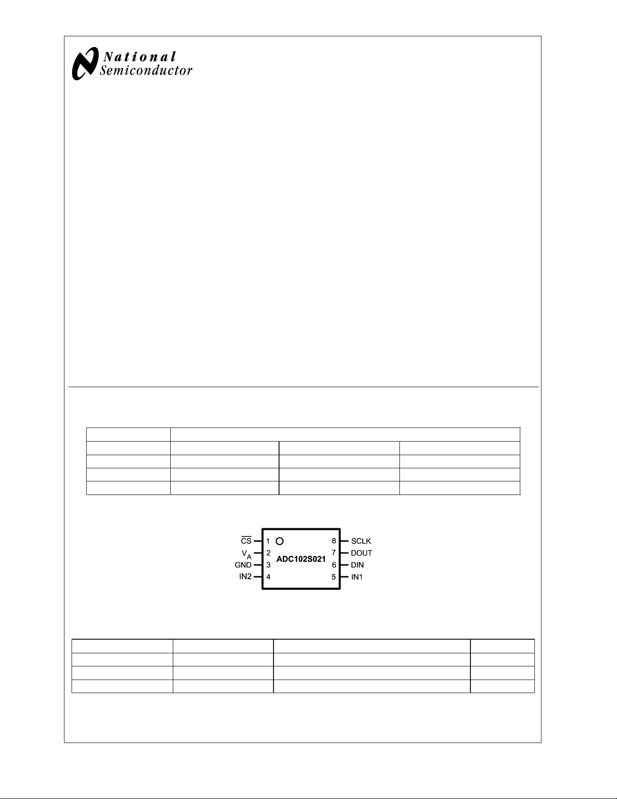
Connection Diagram
20124705
Ordering Information
Order Code Temperature Range Description Top Mark
ADC102S021CIMM −40˚C to +85˚C 8-Lead MSOP Package X17C
ADC102S021CIMMX −40˚C to +85˚C 8-Lead MSOP Package, Tape & Reel X17C
ADC102S021EVAL Evaluation Board
TRI-STATE®is a trademark of National Semiconductor Corporation
™
QSPI
and SPI™are trademarks of Motorola, Inc.
© 2005 National Semiconductor Corporation DS201247 www.national.com
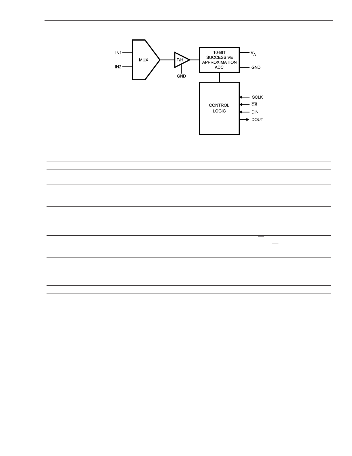
Block Diagram
ADC102S021
Pin Descriptions and Equivalent Circuits
Pin No. Symbol Description
ANALOG I/O
5,4 IN1 and IN2 Analog inputs. These signals can range from 0V to V
DIGITAL I/O
8 SCLK
7 DOUT
6 DIN
1CS
POWER SUPPLY
2V
3 GND The ground return for the analog supply and signals.
A
20124707
.
A
Digital clock input. This clock directly controls the conversion
and readout processes.
Digital data output. The output samples are clocked out of this
pin on falling edges of the SCLK pin.
Digital data input. The ADC102S021’s Control Register is
loaded through this pin on rising edges of the SCLK pin.
Chip select. On the falling edge of CS, a conversion process
begins. Conversions continue as long as CS is held low.
Positive supply pin. This pin should be connected to a quiet
+2.7V to +5.25V source and bypassed to GND witha1µF
capacitor and a 0.1 µF monolithic capacitor located within 1
cm of the power pin.
www.national.com 2
ADC102S021
Absolute Maximum Ratings (Notes 1, 2)
If Military/Aerospace specified devices are required,
please contact the National Semiconductor Sales Office/
Distributors for availability and specifications.
Analog Supply Voltage V
A
Voltage on Any Pin to GND −0.3V to V
Input Current at Any Pin (Note 3)
Package Input Current (Note 3)
Power Consumption at T
= 25˚C See (Note 4)
A
ESD Susceptibility (Note 5)
Human Body Model
Machine Model
Junction Temperature +150˚C
Storage Temperature −65˚C to +150˚C
−0.3V to 6.5V
+0.3V
A
±
10 mA
±
20 mA
2500V
250V
Operating Ratings (Notes 1, 2)
Operating Temperature Range −40˚C ≤ T
V
Supply Voltage +2.7V to +5.25V
A
Digital Input Pins Voltage Range −0.3V to V
Clock Frequency 0.8 to 3.2 MHz
Analog Input Voltage 0V to V
Package Thermal Resistance
Package θ
8-lead MSOP 250˚C / W
Soldering process must comply with National Semiconductor’s Reflow Temperature Profile specifications. Refer to
www.national.com/packaging. (Note 6)
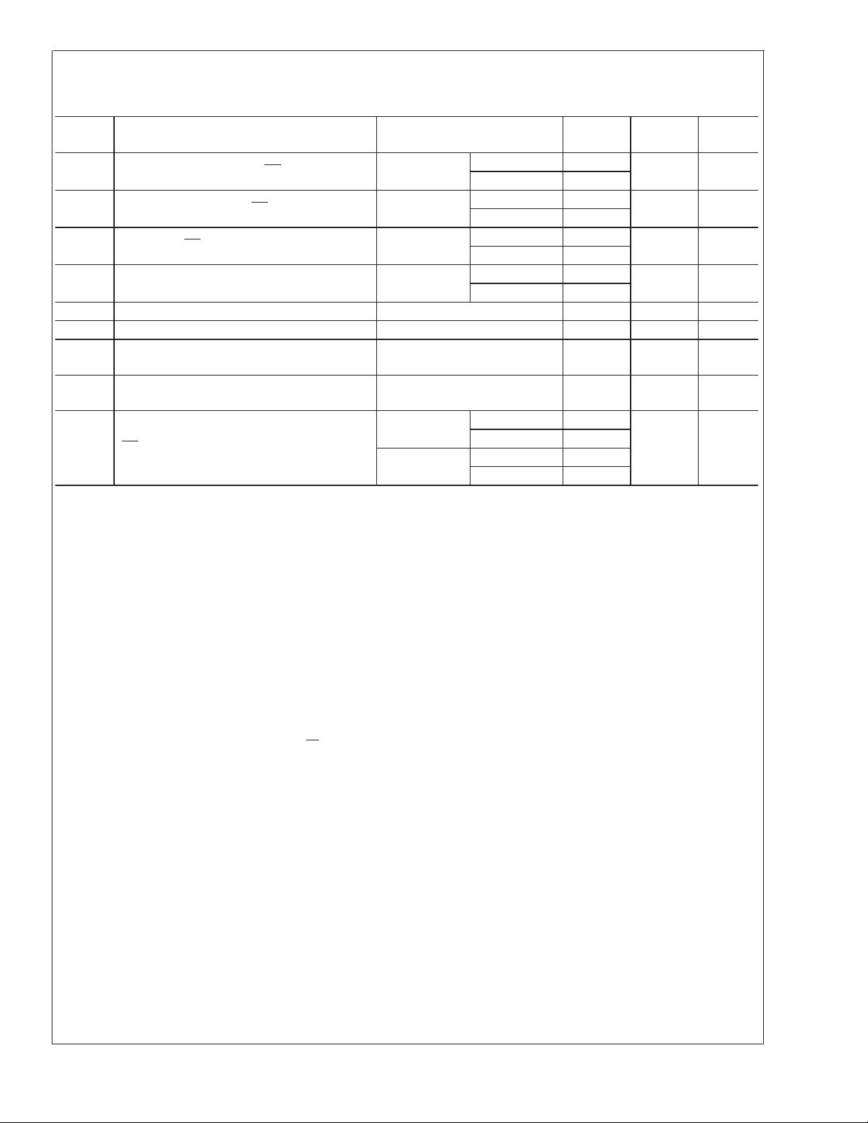
ADC102S021 Converter Electrical Characteristics (Note 9)
The following specifications apply for VA= +2.7V to 5.25V, GND = 0V, CL= 50 pF, f
f
= 50 kSPS to 200 kSPS, unless otherwise noted. Boldface limits apply for TA=T
SAMPLE
25˚C.
Symbol Parameter Conditions Typical
STATIC CONVERTER CHARACTERISTICS
Resolution with No Missing Codes 10 Bits
INL Integral Non-Linearity
DNL Differential Non-Linearity
V
OFF
OEM
Offset Error +0.1
Channel to Channel Offset Error
Match
FSE Full-Scale Error −0.11
FSEM
Channel to Channel Full-Scale Error
Match
DYNAMIC CONVERTER CHARACTERISTICS
V
= +2.7 to 5.25V
SINAD Signal-to-Noise Plus Distortion Ratio
SNR Signal-to-Noise Ratio
THD Total Harmonic Distortion
SFDR Spurious-Free Dynamic Range
ENOB Effective Number of Bits
Channel-to-Channel Crosstalk
Intermodulation Distortion, Second
IMD
Order Terms
Intermodulation Distortion, Third
Order Terms
FPBW -3 dB Full Power Bandwidth
A
= 39.9 kHz, −0.02 dBFS
f
IN
V
= +2.7 to 5.25V
A
= 39.9 kHz, −0.02 dBFS
f
IN
V
= +2.7 to 5.25V
A
= 39.9 kHz, −0.02 dBFS
f
IN
V
= +2.7 to 5.25V
A
= 39.9 kHz, −0.02 dBFS
f
IN
V
= +2.7 to 5.25V
A
= 39.9 kHz, −0.02 dBFS
f
IN
V
= +5.25V
A
= 39.9 kHz
f
IN
V
= +5.25V
A
= 40.161 kHz, fb= 41.015 kHz
f
a
V
= +5.25V
A
= 40.161 kHz, fb= 41.015 kHz
f
a
V
= +5V 11 MHz
A
V
= +3V 8 MHz
A
= 0.8 MHz to 3.2 MHz,
SCLK
MIN
±
0.13
±
0.13
±
0.02
+0.02
61.8 61 dB (min)
61.8 61.3 dB (min)
−86 −72 dB (max)
82 75 dB (min)
9.9 9.8 Bits (min)
−87 dB
−82 dB
−81 dB
JA
to T
: all other limits TA=
MAX
Limits
(Note 9)
+0.3 LSB (max)
−0.4 LSB (min)
±
0.4 LSB (max)
±
0.4 LSB (max)
±
0.5 LSB (max)
±
0.7 LSB (max)
±
0.5 LSB (max)
≤ +85˚C
A
Units
A
A
www.national.com3
ADC102S021 Converter Electrical Characteristics (Note 9) (Continued)
The following specifications apply for VA= +2.7V to 5.25V, GND = 0V, CL= 50 pF, f
f
= 50 kSPS to 200 kSPS, unless otherwise noted. Boldface limits apply for TA=T
SAMPLE
25˚C.
ADC102S021
Symbol Parameter Conditions Typical
ANALOG INPUT CHARACTERISTICS
V
IN
I
DCL
C
INA
DIGITAL INPUT CHARACTERISTICS
V
IH
V
IL
I
IN
C
IND
DIGITAL OUTPUT CHARACTERISTICS
V
OH
V
OL
I
OZH
I
OZL
C
OUT
POWER SUPPLY CHARACTERISTICS (C
V
A
I
A
P
D
AC ELECTRICAL CHARACTERISTICS
f
SCLK
f
S
t
CONV
DC SCLK Duty Cycle f
t
ACQ
Input Range 0 to V
DC Leakage Current
Input Capacitance
Input High Voltage
Track Mode 33 pF
Hold Mode 3 pF
= +5.25V 2.4 V (min)
V
A
V
= +3.6V 2.1 V (min)
A
Input Low Voltage 0.8 V (max)
Input Current VIN=0VorV
A
Digital Input Capacitance 2 4 pF (max)
Output High Voltage
Output Low Voltage
,
TRI-STATE®Leakage Current
I
SOURCE
I
SOURCE
I
SINK
I
SINK
= 200 µA VA− 0.03 VA− 0.5 V (min)
=1mA VA− 0.1 V
= 200 µA 0.03 0.4 V (max)
= 1 mA 0.1 V
TRI-STATE®Output Capacitance 2 4 pF (max)
Output Coding Straight (Natural) Binary
=10pF)
L
Supply Voltage
VA= +5.25V,
Supply Current, Normal Mode
(Operational, CS low)
f
V
f
= 200 kSPS, fIN=40kHz
SAMPLE
= +3.6V,
A
= 200 kSPS, fIN=40kHz
SAMPLE
VA= +5.25V,
Supply Current, Shutdown (CS high)
Power Consumption, Normal Mode
(Operational, CS low)
Power Consumption, Shutdown (CS
high)
f
V
f
VA= +5.25V 6.9 9.5 mW (max)
V
V
V
= 0 kSPS
SAMPLE
= +3.6V,
A
= 0 kSPS
SAMPLE
= +3.6V 1.94 2.5 mW (max)
A
= +5.25V 0.47 µW
A
= +3.6V 0.12 µW
A
Clock Frequency (Note 8)
Sample Rate (Note 8)
Conversion Time 13 SCLK cycles
= 3.2 MHz 50
CLK
Track/Hold Acquisition Time Full-Scale Step Input 3 SCLK cycles
Throughput Time Acquisition Time + Conversion Time 16 SCLK cycles
= 0.8 MHz to 3.2 MHz,
SCLK
±
±
0.01
1.3 1.8 mA (max)
0.55 0.7 mA (max)
MIN
0.1
to T
A
: all other limits TA=
MAX
Limits
(Note 9)
±
1 µA (max)
±
10 µA (max)
±
1 µA (max)
Units
2.7 V (min)
5.25 V (max)
90 nA
32 nA
0.8 MHz (min)
3.2 MHz (max)
50 kSPS (min)
200 kSPS (max)
30 % (min)
70 % (max)
V
www.national.com 4
ADC102S021 Timing Specifications
The following specifications apply for VA= +2.7V to 5.25V, GND = 0V, CL= 50 pF, f
f
SAMPLE
= 50 kSPS to 200 kSPS, Boldface limits apply for TA=T
MIN
to T
: all other limits TA= 25˚C.
MAX
Symbol Parameter Conditions Typical
= +3.0V −3.5
V
t
t
t
CSU
CLH
t
ACC
t
t
t
Setup Time SCLK High to CS Falling Edge (Note 10)
Hold time SCLK Low to CS Falling Edge (Note 10)
Delay from CS Until DOUT active
EN
Data Access Time after SCLK Falling Edge
Data Setup Time Prior to SCLK Rising Edge +3 10 ns (min)
SU
t
Data Valid SCLK Hold Time +3 10 ns (min)
H
SCLK High Pulse Width
CH
SCLK Low Pulse Width
CL
Output Falling
t
DIS
CS Rising Edge to DOUT High-Impedance
Output Rising
Note 1: Absolute Maximum Ratings indicate limits beyond which damage to the device may occur. Operating Ratings indicate conditions for which the device is
functional, but do not guarantee specific performance limits. For guaranteed specifications and test conditions, see the Electrical Characteristics. The guaranteed
specifications apply only for the test conditions listed. Some performance characteristics may degrade when the device is not operated under the listed test
conditions.
Note 2: All voltages are measured with respect to GND = 0V, unless otherwise specified.
Note 3: When the input voltage at any pin exceeds the power supply (that is, V
mA maximum package input current rating limits the number of pins that can safely exceed the power supplies with an input current of 10 mA to two. The Absolute
Maximum Rating specification does not apply to the V
Note 4: The absolute maximum junction temperature (T
junction-to-ambient thermal resistance (θ
for maximum power dissipation listed above will be reached only when the device is operated in a severe fault condition (e.g. when input or output pins are driven
beyond the power supply voltages, or the power supply polarity is reversed). Obviously, such conditions should always be avoided.
Note 5: Human body model is 100 pF capacitor discharged through a 1.5 kΩ resistor. Machine model is 220 pF discharged through zero ohms
Note 6: Reflow temperature profiles are different for lead-free and non-lead-free packages.
Note 7: Tested limits are guaranteed to National’s AOQL (Average Outgoing Quality Level).
Note 8: This is the frequency range over which the electrical performance is guaranteed. The device is functional over a wider range which is specified under
Operating Ratings.
Note 9: Datasheet min/max specification limits are guaranteed by design, test, or statistical analysis.
Note 10: Clock may be in any state (high or low) when CS is asserted, with the restrictions on setup and hold time given by t
), and the ambient temperature (TA), and can be calculated using the formula PDMAX=(TJmax − TA)/θJA. The values
JA
pin. The current into the VApin is limited by the Analog Supply Voltage specification.
A
max) for this device is 150˚C. The maximum allowable power dissipation is dictated by TJmax, the
J
IN
<
GND or V
A
V
= +5.0V −0.5
A
= +3.0V +4.5
V
A
V
= +5.0V +1.5
A
VA= +3.0V +4
V
= +5.0V +2
A
= +3.0V +16.5
V
A
V
= +5.0V +15
A
= +3.0V 1.7
V
A
V
= +5.0V 1.2
A
V
= +3.0V 1.0
A
V
= +5.0V 1.0
A
>
VA), the current at that pin should be limited to 10 mA. The 20
IN
= 0.8 MHz to 3.2 MHz,
SCLK
0.5 x
t
SCLK
0.5 x
t
SCLK
CSU
and t
Limits
(Note 7)
0.3 x
t
SCLK
0.3 x
t
SCLK
.
CLH
Units
10 ns (min)
10 ns (min)
30
30
(max)
(max)
ns (min)
ns (min)
20
(max)
ADC102S021
ns
ns
ns
www.national.com5
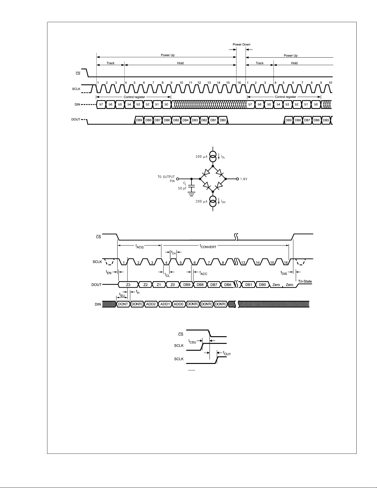
Timing Diagrams
ADC102S021
ADC102S021 Operational Timing Diagram
20124708
Timing Test Circuit
20124751
ADC102S021 Serial Timing Diagram
SCLK and CS Timing Parameters
www.national.com 6
20124706
20124750

Specification Definitions
ACQUISITION TIME is the time required to acquire the input
voltage. That is, it is time required for the hold capacitor to
charge up to the input voltage.
APERTURE DELAY is the time between the fourth falling
SCLK edge of a conversion and the time when the input
signal is acquired or held for conversion.
CONVERSION TIME is the time required, after the input
voltage is acquired, for the ADC to convert the input voltage
to a digital word.
CROSSTALK is the coupling of energy from one channel
into the other channel, or the amount of signal energy from
one analog input that appears at the measured analog input.
DIFFERENTIAL NON-LINEARITY (DNL) is the measure of
the maximum deviation from the ideal step size of 1 LSB.
DUTY CYCLE is the ratio of the time that a repetitive digital
waveform is high to the total time of one period. The specification here refers to the SCLK.
EFFECTIVE NUMBER OF BITS (ENOB, or EFFECTIVE
BITS) is another method of specifying Signal-to-Noise and
Distortion or SINAD. ENOB is defined as
(SINAD − 1.76) / 6.02 and says that the converter is equivalent to a perfect ADC of this (ENOB) number of bits.
FULL POWER BANDWIDTH is a measure of the frequency
at which the reconstructed output fundamental drops 3 dB
below its low frequency value for a full scale input.
GAIN ERROR is the deviation of the last code transition
(111...110) to (111...111) from the ideal (V
after adjusting for offset error.
INTEGRAL NON-LINEARITY (INL) is a measure of the
deviation of each individual code from a line drawn from
negative full scale (
through positive full scale (
1
⁄2LSB below the first code transition)
1
⁄2LSB above the last code
transition). The deviation of any given code from this straight
line is measured from the center of that code value.
INTERMODULATION DISTORTION (IMD) is the creation of
additional spectral components as a result of two sinusoidal
frequencies being applied to the ADC input at the same time.
It is defined as the ratio of the power in the second and third
order intermodulation products to the sum of the power in
both of the original frequencies. IMD is usually expressed in
dB.
− 1.5 LSB),
REF
MISSING CODES are those output codes that will never
appear at the ADC outputs. The ADC102S021 is guaranteed
not to have any missing codes.
OFFSET ERROR is the deviation of the first code transition
(000...000) to (000...001) from the ideal (i.e. GND + 0.5
LSB).
SIGNAL TO NOISE RATIO (SNR) is the ratio, expressed in
dB, of the rms value of the input signal to the rms value of the
sum of all other spectral components below one-half the
sampling frequency, not including harmonics or d.c.
SIGNAL TO NOISE PLUS DISTORTION (S/N+D or SINAD)
Is the ratio, expressed in dB, of the rms value of the input
signal to the rms value of all of the other spectral components below half the clock frequency, including harmonics
but excluding d.c.
SPURIOUS FREE DYNAMIC RANGE (SFDR) is the difference, expressed in dB, between the rms values of the input
signal and the peak spurious signal where a spurious signal
is any signal present in the output spectrum that is not
present at the input, excluding d.c.
TOTAL HARMONIC DISTORTION (THD) is the ratio, expressed in dB or dBc, of the rms total of the first five
harmonic components at the output to the rms level of the
input signal frequency as seen at the output. THD is calculated as
where Af1is the RMS power of the input frequency at the
output and Af
through Af6are the RMS power in the first 5
2
harmonic frequencies.
THROUGHPUT TIME is the minimum time required between
the start of two successive conversion. It is the acquisition
time plus the conversion time. In the case of the
ADC102S021, this is 16 SCLK periods.
ADC102S021
www.national.com7

Typical Performance Characteristics T
= 0.8 MHz to 3.2 MHz, fIN= 39.9 kHz unless otherwise stated.
f
SCLK
DNL-V
ADC102S021
DNL-VA= 5.0V INL - VA= 5.0V
= 3.0V INL - VA= 3.0V
A
20124720 20124721
= +25˚C, f
A
SAMPLE
= 50 kSPS to 200 kSPS,
20124762 20124763
DNL vs. Supply INL vs. Supply
20124722 20124723
www.national.com 8

ADC102S021
Typical Performance Characteristics T
= 0.8 MHz to 3.2 MHz, fIN= 39.9 kHz unless otherwise stated. (Continued)
f
SCLK
= +25˚C, f
A
DNL vs. Clock Frequency INL vs. Clock Frequency
20124724 20124725
DNL vs. Clock Duty Cycle INL vs. Clock Duty Cycle
= 50 kSPS to 200 kSPS,
SAMPLE
20124726 20124727
DNL vs. Temperature INL vs. Temperature
20124728 20124729
www.national.com9

Typical Performance Characteristics T
= 0.8 MHz to 3.2 MHz, fIN= 39.9 kHz unless otherwise stated. (Continued)
f
SCLK
= +25˚C, f
A
= 50 kSPS to 200 kSPS,
SAMPLE
ADC102S021
SNR vs. Supply THD vs. Supply
20124730 20124735
SNR vs. Clock Frequency THD vs. Clock Frequency
20124731 20124736
SNR vs. Clock Duty Cycle THD vs. Clock Duty Cycle
20124732 20124737
www.national.com 10

ADC102S021
Typical Performance Characteristics T
= 0.8 MHz to 3.2 MHz, fIN= 39.9 kHz unless otherwise stated. (Continued)
f
SCLK
= +25˚C, f
A
SNR vs. Input Frequency THD vs. Input Frequency
20124733 20124738
SNR vs. Temperature THD vs. Temperature
= 50 kSPS to 200 kSPS,
SAMPLE
20124734 20124739
SFDR vs. Supply SINAD vs. Supply
20124740 20124745
www.national.com11

Typical Performance Characteristics T
= 0.8 MHz to 3.2 MHz, fIN= 39.9 kHz unless otherwise stated. (Continued)
f
SCLK
= +25˚C, f
A
= 50 kSPS to 200 kSPS,
SAMPLE
ADC102S021
SFDR vs. Clock Frequency SINAD vs. Clock Frequency
20124741 20124746
SFDR vs. Clock Duty Cycle SINAD vs. Clock Duty Cycle
20124742 20124747
SFDR vs. Input Frequency SINAD vs. Input Frequency
20124743 20124748
www.national.com 12

ADC102S021
Typical Performance Characteristics T
= 0.8 MHz to 3.2 MHz, fIN= 39.9 kHz unless otherwise stated. (Continued)
f
SCLK
= +25˚C, f
A
SFDR vs. Temperature SINAD vs. Temperature
20124744 20124749
ENOB vs. Supply ENOB vs. Clock Frequency
= 50 kSPS to 200 kSPS,
SAMPLE
20124752 20124753
ENOB vs. Clock Duty Cycle ENOB vs. Input Frequency
20124754 20124755
www.national.com13

Typical Performance Characteristics T
= 0.8 MHz to 3.2 MHz, fIN= 39.9 kHz unless otherwise stated. (Continued)
f
SCLK
= +25˚C, f
A
= 50 kSPS to 200 kSPS,
SAMPLE
ADC102S021
ENOB vs. Temperature Spectral Response - 3V, 200 ksps
20124756 20124759
Spectral Response - 5V, 200 ksps Power Consumption vs. Throughput
20124760 20124761
www.national.com 14

Applications Information
1.0 ADC102S021 OPERATION
The ADC102S021 is a successive-approximation analog-todigital converter designed around a charge-redistribution
digital-to-analog converter. Simplified schematics of the
ADC102S021 in both track and hold modes are shown in
Figures 1, 2, respectively. In Figure 1, the ADC102S021 is in
track mode: switch SW1 connects the sampling capacitor to
one of two analog input channels through the multiplexer,
and SW2 balances the comparator inputs. The
ADC102S021 is in this state for the first three SCLK cycles
after CS is brought low.
Figure 2 shows the ADC102S021 in hold mode: switch SW1
connects the sampling capacitor to ground, maintaining the
ADC102S021
sampled voltage, and switch SW2 unbalances the comparator. The control logic then instructs the charge-redistribution
DAC to add fixed amounts of charge to the sampling capacitor until the comparator is balanced. When the comparator is
balanced, the digital word supplied to the DAC is the digital
representation of the analog input voltage. The
ADC102S021 is in this state for the fourth through sixteenth
SCLK cycles after CS is brought low.
The time when CS is low is considered a serial frame. Each
of these frames should contain an integer multiple of 16
SCLK cycles, during which time a conversion is performed
and clocked out at the DOUT pin and data is clocked into the
DIN pin to indicate the multiplexer address for the next
conversion.
FIGURE 1. ADC102S021 in Track Mode
FIGURE 2. ADC102S021 in Hold Mode
2.0 USING THE ADC102S021
An ADC102S021 timing diagram and a serial interface timing
diagram for the ADC102S021 are shown in the Timing Diagrams section. CS is chip select, which initiates conversions
and frames the serial data transfers. SCLK (serial clock)
controls both the conversion process and the timing of serial
data. DOUT is the serial data output pin, where a conversion
result is sent as a serial data stream, MSB first. Data to be
written to the ADC102S021’s Control Register is placed on
DIN, the serial data input pin. New data is written to DIN with
each conversion.
A serial frame is initiated on the falling edge of CS and ends
on the rising edge of CS. Each frame must contain an integer
multiple of 16 rising SCLK edges. The ADC output data
(DOUT) is in a high impedance state when CS is high and is
active when CS is low. Thus, CS acts as an output enable.
Additionally, the device goes into a power down state when
CS is high and also between continuous conversion cycles.
20124709
20124710
During the first 3 cycles of SCLK, the ADC is in the track
mode, acquiring the input voltage. For the next 13 SCLK
cycles the conversion is accomplished and the data is
clocked out, MSB first, starting at the 5th clock. If there is
more than one conversion in a frame, the ADC will re-enter
the track mode on the falling edge of SCLK after the N*16th
rising edge of SCLK, and re-enter the hold/convert mode on
the N*16+4th falling edge of SCLK, where "N" is an integer.
When CS is brought high, SCLK is internally gated off. If
SCLK is stopped in the low state while CS is high, the
subsequent fall of CS will generate a falling edge of the
internal version of SCLK, putting the ADC into the track
mode. This is seen by the ADC as the first falling edge of
SCLK. If SCLK is stopped with SCLK high, the ADC enters
the track mode on the first falling edge of SCLK after the
falling edge of CS.
During each conversion, data is clocked into the DIN pin on
the first 8 rising edges of SCLK after the fall of CS. For each
www.national.com15

Applications Information (Continued)
conversion, it is necessary to clock in the data indicating the
input that is selected for the conversion after the current one.
See Tables 1, 2 and Table 3.
ADC102S021
If CS and SCLK go low simultaneously, it is the following
rising edge of SCLK that is considered the first rising edge
for clocking data into DIN.
Bit 7 (MSB) Bit 6 Bit 5 Bit 4 Bit 3 Bit 2 Bit 1 Bit 0
DONTC DONTC ADD2 ADD1 ADD0 DONTC DONTC DONTC
TABLE 2. Control Register Bit Descriptions
Bit #: Symbol: Description
7-6,2-0 DONTC Don’t care. The value of these bits do not affect the device.
3 ADD0 These bits determine which input channel will be sampled and converted in
4 ADD1
5 ADD2
ADD2 ADD1 ADD0 Input Channel
x 0 0 IN1 (Default)
x 0 1 IN2
x 1 x Not allowed. The output signal at the D
the next track/hold cycle. The mapping between codes and channels is
shown in Table 3.
TABLE 3. Input Channel Selection
There are no power-up delays or dummy conversions required with the ADC102S021. The ADC is able to sample
and convert an input to full conversion immediately following
power up. The first conversion result after power-up will be
that of IN1.
TABLE 1. Control Register Bits
OUT
pin is indeterminate if ADD1 is high.
www.national.com 16

Applications Information (Continued)
3.0 ADC102S021 TRANSFER FUNCTION
The output format of the ADC102S021 is straight binary. Code transitions occur midway between successive integer LSB values.
The LSB width for the ADC102S021 is V
output code of 00 0000 0000 to a code of 00 0000 0001 is at 1/2 LSB, or a voltage of V
steps of one LSB.
/1024. The ideal transfer characteristic is shown in Figure 3. The transition from an
A
/2048. Other code transitions occur at
A
20124711
ADC102S021
FIGURE 3. Ideal Transfer Characteristic
4.0 TYPICAL APPLICATION CIRCUIT
A typical application of the ADC102S021 is shown in Figure
4. Power is provided in this example by the National Semi-
conductor LP2950 low-dropout voltage regulator, available in
a variety of fixed and adjustable output voltages. The power
supply pin is bypassed with a capacitor network located
close to the ADC102S021. Because the reference for the
ADC102S021 is the supply voltage, any noise on the supply
will degrade device noise performance. To keep noise off the
supply, use a dedicated linear regulator for this device, or
provide sufficient decoupling from other circuitry to keep
noise off the ADC102S021 supply pin. Because of the
ADC102S021’s low power requirements, it is also possible to
use a precision reference as a power supply to maximize
performance. The four-wire interface is also shown connected to a microprocessor or DSP.
20124713
FIGURE 4. Typical Application Circuit
www.national.com17

Applications Information (Continued)
5.0 ANALOG INPUTS
An equivalent circuit for one of the ADC102S021’s input
channels is shown in Figure 5. Diodes D1 and D2 provide
ADC102S021
ESD protection for the analog inputs. At no time should any
input go beyond (V
ESD diodes will begin conducting, which could result in
erratic operation.
The capacitor C1 in Figure 5 has a typical value of 3 pF, and
is mainly the package pin capacitance. Resistor R1 is the on
resistance of the multiplexer and track / hold switch, and is
typically 500 ohms. Capacitor C2 is the ADC102S021 sampling capacitor and is typically 30 pF. The ADC102S021 will
deliver best performance when driven by a low-impedance
source to eliminate distortion caused by the charging of the
sampling capacitance. This is especially important when
using the ADC102S021 to sample AC signals. Also important
when sampling dynamic signals is a band-pass or low-pass
filter to reduce harmonics and noise, improving dynamic
performance.
+ 300 mV) or (GND − 300 mV), as these
A
The user may trade off throughput for power consumption by
simply performing fewer conversions per unit time. The
Power Consumption vs. Sample Rate curve in the Typical
Performance Curves section shows the typical power consumption of the ADC102S021 versus throughput. To calculate the power consumption, simply multiply the fraction of
time spent in the normal mode by the normal mode power
consumption , and add the fraction of time spent in shutdown
mode multiplied by the shutdown mode power dissipation.
7.1 Power Management
When the ADC102S021 is operated continuously in normal
mode, the maximum throughput is f
may be traded for power consumption by running f
/16. Throughput
SCLK
SCLK
at its
maximum 3.2 MHz and performing fewer conversions per
unit time, putting the ADC102S021 into shutdown mode
between conversions. A plot of typical power consumption
versus throughput is shown in the Typical Performance
Curves section. To calculate the power consumption for a
given throughput, multiply the fraction of time spent in the
normal mode by the normal mode power consumption and
add the fraction of time spent in shutdown mode multiplied
by the shutdown mode power consumption. Generally, the
user will put the part into normal mode and then put the part
back into shutdown mode. Note that the curve of power
consumption vs. throughput is nearly linear. This is because
the power consumption in the shutdown mode is so small
that it can be ignored for all practical purposes.
20124714
FIGURE 5. Equivalent Input Circuit
6.0 DIGITAL INPUTS AND OUTPUTS
The ADC102S021’s digital output DOUT is limited by, and
cannot exceed, the supply voltage, V
. The digital input pins
A
are not prone to latch-up and, and although not recommended, SCLK, CS and DIN may be asserted before V
without any latchup risk.
7.0 POWER SUPPLY CONSIDERATIONS
The ADC102S021 is fully powered-up whenever CS is low,
and fully powered-down whenever CS is high, with one
exception: the ADC102S021 automatically enters powerdown mode between the 16th falling edge of a conversion
and the 1st falling edge of the subsequent conversion (see
Timing Diagrams).
The ADC102S021 can perform multiple conversions back to
back; each conversion requires 16 SCLK cycles. The
ADC102S021 will perform conversions continuously as long
as CS is held low.
7.2 Power Supply Noise Considerations
The charging of any output load capacitance requires current from the power supply, V
. The current pulses required
A
from the supply to charge the output capacitance will cause
voltage variations on the supply. If these variations are large
enough, they could degrade SNR and SINAD performance
of the ADC. Furthermore, discharging the output capacitance when the digital output goes from a logic high to a logic
low will dump current into the die substrate, which is resistive. Load discharge currents will cause "ground bounce"
noise in the substrate that will degrade noise performance if
that current is large enough. The larger is the output capaci-
A
tance, the more current flows through the die substrate and
the greater is the noise coupled into the analog channel,
degrading noise performance.
To keep noise out of the power supply, keep the output load
capacitance as small as practical. If the load capacitance is
greater than 50 pF, use a 100 Ω series resistor at the ADC
output, located as close to the ADC output pin as practical.
This will limit the charge and discharge current of the output
capacitance and improve noise performance.
www.national.com 18

Physical Dimensions inches (millimeters) unless otherwise noted
ADC102S021 2 Channel, 200 KSPS, 10-Bit A/D Converter
8-Lead MSOP
Order Number ADC102S021CIMM, ADC102S021CIMMX
NS Package Number P0MUA08A
National does not assume any responsibility for use of any circuitry described, no circuit patent licenses are implied and National reserves
the right at any time without notice to change said circuitry and specifications.
For the most current product information visit us at www.national.com.
LIFE SUPPORT POLICY
NATIONAL’S PRODUCTS ARE NOT AUTHORIZED FOR USE AS CRITICAL COMPONENTS IN LIFE SUPPORT DEVICES OR SYSTEMS
WITHOUT THE EXPRESS WRITTEN APPROVAL OF THE PRESIDENT AND GENERAL COUNSEL OF NATIONAL SEMICONDUCTOR
CORPORATION. As used herein:
1. Life support devices or systems are devices or systems
which, (a) are intended for surgical implant into the body, or
(b) support or sustain life, and whose failure to perform when
properly used in accordance with instructions for use
2. A critical component is any component of a life support
device or system whose failure to perform can be reasonably
expected to cause the failure of the life support device or
system, or to affect its safety or effectiveness.
provided in the labeling, can be reasonably expected to result
in a significant injury to the user.
BANNED SUBSTANCE COMPLIANCE
National Semiconductor manufactures products and uses packing materials that meet the provisions of the Customer Products
Stewardship Specification (CSP-9-111C2) and the Banned Substances and Materials of Interest Specification (CSP-9-111S2) and contain
no ‘‘Banned Substances’’ as defined in CSP-9-111S2.
National Semiconductor
Americas Customer
Support Center
Email: new.feedback@nsc.com
Tel: 1-800-272-9959
www.national.com
National Semiconductor
Europe Customer Support Center
Fax: +49 (0) 180-530 85 86
Email: europe.support@nsc.com
Deutsch Tel: +49 (0) 69 9508 6208
English Tel: +44 (0) 870 24 0 2171
Français Tel: +33 (0) 1 41 91 8790
National Semiconductor
Asia Pacific Customer
Support Center
Email: ap.support@nsc.com
National Semiconductor
Japan Customer Support Center
Fax: 81-3-5639-7507
Email: jpn.feedback@nsc.com
Tel: 81-3-5639-7560
 Loading...