November 1999
ADC10154/ADC10158
10-Bit Plus Sign 4 µs ADCs with 4- or 8-Channel MUX,
Track/Hold and Reference
ADC10154/ADC10158 10-Bit Plus Sign 4 µs ADCs with 4- or 8-Channel MUX, Track/Hold and
Reference
General Description
The ADC10154 and ADC10158 are CMOS 10-bit plus sign
successive approximationA/D converters with versatile analog input multiplexers, track/hold function and a 2.5V
band-gap reference. The 4-channel or 8-channel multiplexers can be software configured for single-ended, differential
or pseudo-differential modes of operation.
The input track/hold is implemented using a capacitive array
and sampled-data comparator.
Resolution can be programmed to be 8-bit, 8-bit plus sign,
10-bit or 10-bit plus sign. Lower-resolution conversions can
be performed faster.
The variable resolution output data word is read in two bytes,
and can be formatted left justified or right justified, high byte
first.
Applications
n Process control
n Instrumentation
n Test equipment
Features
n 4- or 8- channel configurable multiplexer
n Analog input track/hold function
n 0V to 5V analog input range with single +5V power
supply
n −5V to +5V analog input voltage range with
supplies
n Fully tested in unipolar (single +5V supply) and bipolar
n Programmable resolution/speed and output data format
n Ratiometric or Absolute voltage reference operation
n No zero or full scale adjustment required
n No missing codes over temperature
n Easy microprocessor interface
±
(dual
5V supplies) operation
±
5V
Key Specifications
n Resolution 10-bit plus sign
n Integral linearity error
n Unipolar power dissipation 33 mW (max)
n Conversion time (10-bit + sign) 4.4 µs (max)
n Conversion time (8-bit) 3.2 µs (max)
n Sampling rate (10-bit + sign) 166 kHz
n Sampling rate (8-bit) 207 kHz
n Band-gap reference 2.5V
±
1 LSB (max)
±
2.0% (max)
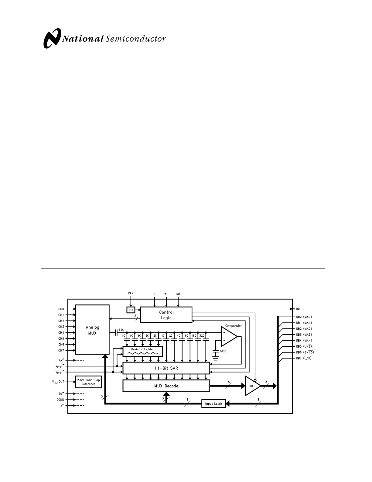
ADC10158 Simplified Block Diagram
DS011225-1
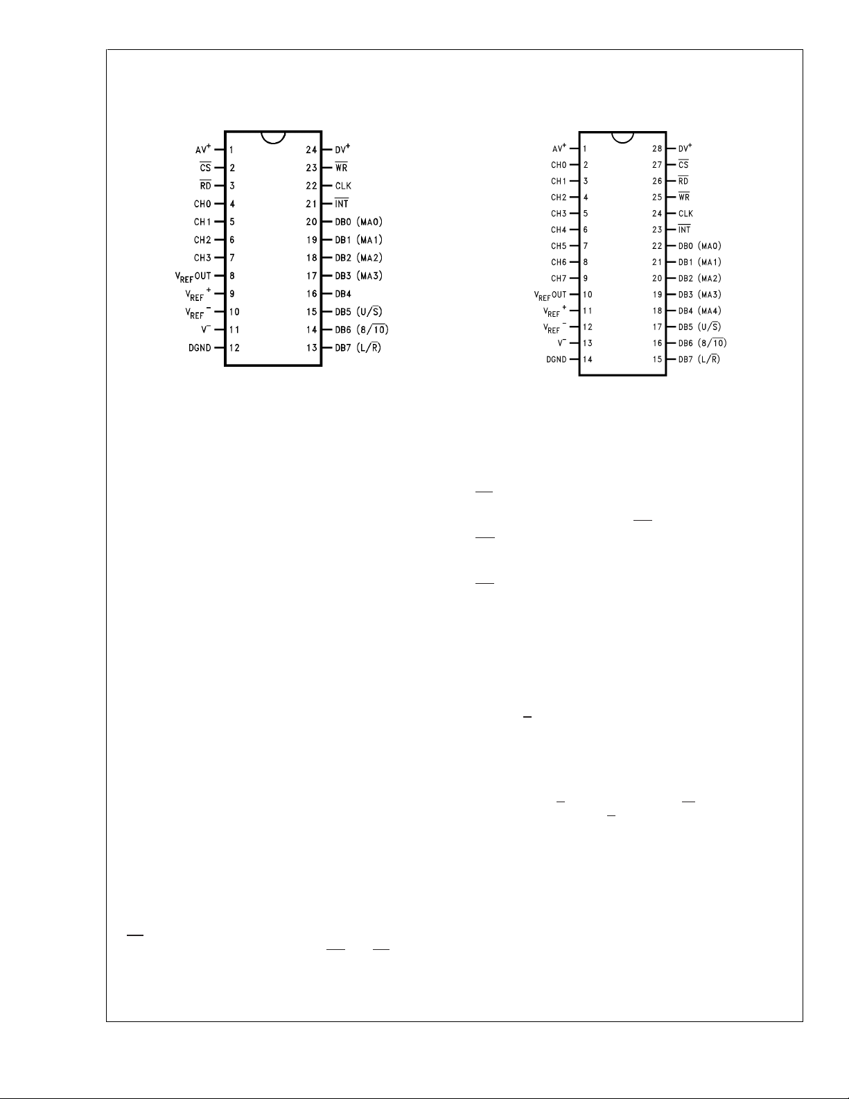
Connection Diagrams
Dual-in-Line and SO Packages
ADC10154/ADC10158
DS011225-2
Top View
Order Number ADC10154
NS Package Number M24B
Pin Descriptions
+
AV
+
DV
DGND This is the digital ground. All logic levels are
−
V
+
V
REF
−
V
REF
V
Out This is the internal band-gap voltage reference
REF
CS
This is the positive analog supply. This pin
should be bypassed with a 0.1 µF ceramic capacitor and a 10 µF tantalum capacitor to the
system analog ground.
This is the positive digital supply. This supply
pin also needs to be bypassed with 0.1 µF
ceramic and 10 µF tantalum capacitors to the
system digital ground. AV
+
and DV+should be
bypassed separately and tied to same power
supply.
referred to this ground.
This is the negative analogsupply.For unipolar
operation this pin may be tied to the system
analog ground or to a negative supply source.
It should not go above DGND by more than
50 mV. When bipolar operation is required, the
voltage on this pin will limit the analog input’s
negative voltage level. In bipolar operation this
supply pin needs to be bypassed with 0.1 µF
ceramic and 10 µF tantalum capacitors to the
system analog ground.
,
These are the positive and negative reference
inputs. The voltage difference between V
and V
−
will set the analog input voltage
REF
span.
output. For proper operation of the voltage reference, this pin needs to be bypassed with a
330 µF tantalum or electrolytic capacitor.
This is the chip select input. When a logic low
is applied to this pin the WR and RD pins are
enabled.
REF
Dual-in-Line and SO Packages
DS011225-3
Top View
Order Number ADC10158
NS Package Numbers
M28B or N28B
RD
This is the read control input. When a logic low
is applied to this pin the digital outputs are
enabled and the INT output is reset high.
WR This is the write control input. The rising edge
of the signal applied to this pin selects the
multiplexer channel and initiates a conversion.
INT
This is the interrupt output. A logic low at this
output indicates the completion of a conversion.
CLK This is the clock input. The clock frequency
directly controls the duration of the conversion
time (for example, in the 10-bit bipolar mode
t
DB0(MA0)
–DB7 (L/R)
= 22/f
C
6/f
CLK
These are the digital data inputs/outputs. DB0
is the least significant bit of the digital output
) and the acquisition time (tA=
CLK
).
word; DB7 is the most significant bit in the
digital output word (see the Output Data Configuration table). MA0 through MA4 are the
digital inputs for the multiplexer channel selection (see the Multiplexer Addressing tables).
U/S (Unsigned/Signed), 8/10, (8/10-bit resolu-
+
tion) and L/R (Left/Right justification) are the
digital input bits that set the A/D’s output word
format and resolution (see the Output Data
Configuration table). The conversion time is
modified by the chosen resolution (see Electrical AC Characteristics table). The lower the
resolution, the faster the conversion will be.
CH0–CH7 These are the analog input multiplexer chan-
nels. They can be configured as single-ended
inputs, differential input pairs, or
pseudo-differential inputs (see the Multiplexer
Addressing tables for the input polarity
assignments).
www.national.com 2
ADC10154/ADC10158
Absolute Maximum Ratings (Notes 1, 3)
If Military/Aerospace specified devices are required,
please contact the National Semiconductor Sales Office/
Distributors for availability and specifications.
Positive Supply Voltage
+
(V
=AV+=DV+) 6.5V
Negative Supply Voltage (V
Total Supply Voltage (V
Total Reference Voltage
(V
REF
+
−V
−
) 6.6V
REF
Voltage at Inputs and
Outputs V
Input Current at Any Pin (Note 4)
Package Input Current (Note 4)
Package Dissipation at
= 25˚C (Note 5) 500 mW
T
A
ESD Susceptibility (Note 6) 2000V
Soldering Information
N Packages (10 Sec) 260˚C
J Packages (10 Sec) 300˚C
SO Package (Note 7):
Vapor Phase (60 Sec) 215˚C
Infrared (15 Sec) 220˚C
−
) −6.5V
+−V−
) 13V
−
− 0.3V to V++ 0.3V
±
5mA
±
20 mA
Storage Temperature
Ceramic DIP Packages
Plastic DIP and SO Packages
−65˚C to +150˚C
−40˚C to +150˚C
Operating Ratings (Notes 2, 3)
Temperature Range T
ADC10154CIWM,
ADC10158CIN,
ADC10158CIWM −40˚C ≤ T
Positive Supply
Voltage
+
=AV+=DV+) 4.5 VDCto 5.5 V
(V
Unipolar Negative
Supply Voltage
−
) DGND
(V
Bipolar Negative
Supply Voltage
−
) −4.5V to −5.5V
(V
+−V−
V
+
V
REF
−
V
REF
V
REF
(V
REF
+
−V
−
) 0.5 VDCto V
REF
AV++ 0.05 VDCto V−− 0.05 V
AV++ 0.05 VDCto V−− 0.05 V
MIN
≤ TA≤ T
≤ +85˚C
A
MAX
DC
11V
DC
DC
+
Electrical Characteristics
The following specifications apply for V+=AV+=DV+= + 5.0 VDC,V
operation or V
=TJ=T
−
= −5.0 VDCfor bipolar operation, and f
MIN
to T
; all other limits TA=TJ= 25˚C. (Notes 8, 9, 12)
MAX
= 5.0 MHz unless otherwise specified. Boldface limits apply for T
CLK
Symbol Parameter Conditions Typical
UNIPOLAR CONVERTER AND MULTIPLEXER STATIC CHARACTERISTICS
Resolution 10 + Sign Bits
Unipolar Integral V
Linearity Error V
Unipolar Full-Scale Error V
Unipolar Offset Error V
Unipolar Total Unadjusted V
Error (Note 13) V
Unipolar Power Supply V
Sensitivity V
+
= 2.5V
REF
+
= 5.0V
REF
+
= 2.5V
REF
+
V
= 5.0V
REF
+
= 2.5V
REF
+
V
= 5.0V
REF
+
= 2.5V
REF
+
= 5.0V
REF
+
= +5V±10%
+
= 4.5V
REF
Offset Error
Full-Scale Error
Integral Linearity Error
BIPOLAR CONVERTER AND MULTIPLEXER STATIC CHARACTERISTICS
Resolution 10 + Sign Bits
Bipolar Integral V
REF
+
= 5.0V
Linearity Error
Bipolar Full-Scale Error V
REF
+
= 5.0V
+
= 5.000 VDC,V
REF
(Note 10)
±
0.5 LSB
±
0.5 LSB
±
1 LSB
±
1.5 LSB
±
0.25
±
0.25
±
0.25 LSB
−
= GND, V−= GND for unipolar
REF
CIN and CIWM Units
Suffixes
(Limit)
Limits
(Note 11)
±
1 LSB (Max)
±
1.5 LSB (Max)
±
2 LSB (Max)
±
2.5 LSB (Max)
±
1 LSB (Max)
±
1 LSB (Max)
±
1 LSB (Max)
±
1.25 LSB (Max)
A
www.national.com3
Electrical Characteristics (Continued)
The following specifications apply for V+=AV+=DV+= + 5.0 VDC,V
operation or V
=TJ=T
−
= −5.0 VDCfor bipolar operation, and f
MIN
to T
; all other limits TA=TJ= 25˚C. (Notes 8, 9, 12)
MAX
= 5.0 MHz unless otherwise specified. Boldface limits apply for T
CLK
Symbol Parameter Conditions Typical
ADC10154/ADC10158
BIPOLAR CONVERTER AND MULTIPLEXER STATIC CHARACTERISTICS
Bipolar Negative Full-Scale V
Error with Positive-Full
Scale Adjusted
Bipolar Offset Error V
Bipolar Total Unadjusted V
Error (Note 13)
Bipolar Power Supply
Sensitivity
Offset Error V
Full-Scale Error V
Integral Linearity Error
Offset Error V
Full-Scale Error V
Integral Linearity Error
UNIPOLAR AND BIPOLAR CONVERTER AND MULTIPLEXER STATIC CHARACTERISTICS
Missing Codes 0
DC Common Mode V
Error (Note 14) = VINwhere
Bipolar +5.0V ≥ V
Unipolar +5.0V ≥ V
R
REF
C
REF
V
AI
C
AI
Reference Input Resistance 7 4.5 kΩ (Max)
Reference Input Capacitance 70 pF
Analog Input Voltage (V++0.05) V (Max)
Analog Input Capacitance 30 pF
Off Channel Leakage On Channel = 5V −400 −1000 nA (Max)
Current Off Channel = 0V
(Note 15) On Channel = 0V 400 1000 nA (Max)
+
= 5.0V
REF
+
= 5.0V
REF
+
= 5.0V
REF
+
= +5V±10%
+
= 4.5V
REF
−
= −5V±10%
+
= 4.5V
REF
+
−
=V
IN
IN
≥ −5.0V
IN
≥ 0V
IN
Off Channel = 5V
+
= 5.000 VDC,V
REF
(Note 10)
±
0.5
±
0.5
±
0.25 LSB
±
0.25
±
0.25
±
0.25 LSB
±
0.25
±
0.25
−
= GND, V−= GND for unipolar
REF
CIN and CIWM Units
Suffixes
(Limit)
Limits
(Note 11)
±
1.25 LSB (Max)
±
2.5 LSB (Max)
±
3 LSB (Max)
±
2.5 LSB (Max)
±
1.5 LSB (Max)
±
0.75 LSB (Max)
±
0.75 LSB (Max)
±
0.75 LSB (Max)
±
0.5 LSB (Max)
9.5 kΩ (Max)
−
(V
−0.05) V (Min)
A
Electrical Characteristics
The following specifications apply for V+=AV+=DV+= + 5.0 VDC,V
operation or V
=TJ=T
−
= −5.0 VDCfor bipolar operation, and f
MIN
to T
; all other limits TA=TJ= 25˚C. (Notes 8, 9, 12)
MAX
= 5.0 MHz unless otherwise specified. Boldface limits apply for T
CLK
+
= 5.000 VDC,V
REF
Symbol Parameter Conditions Typical Limits
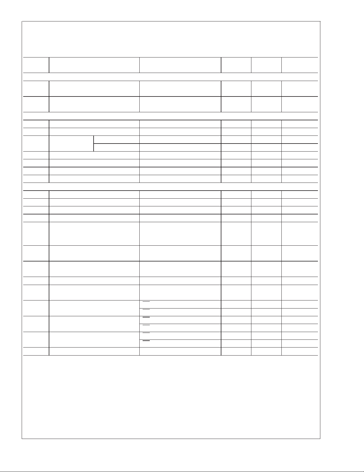
DYNAMIC CONVERTER AND MULTIPLEXER CHARACTERISTICS
S/(N+D) Unipolar Signal-to-Noise+ f
Distortion Ratio f
S/(N+D) Bipolar Signal-to-Noise+ f
Distortion Ratio f
www.national.com 4
= 10 kHz, VIN= 4.85 V
IN
= 150 kHz, VIN= 4.85 V
IN
= 10 kHz, VIN=±4.85V 60 dB
IN
= 150 kHz, VIN=±4.85V 58 dB
IN
p–p
p-p
−
= GND, V−= GND for unipolar
REF
(Note 10)
(Note 11)
60 dB
58 dB
A
Units
(Limit)
Electrical Characteristics (Continued)
The following specifications apply for V+=AV+=DV+= + 5.0 VDC,V
operation or V
=TJ=T
−
= −5.0 VDCfor bipolar operation, and f
MIN
to T
; all other limits TA=TJ= 25˚C. (Notes 8, 9, 12)
MAX
= 5.0 MHz unless otherwise specified. Boldface limits apply for T
CLK
+
= 5.000 VDC,V
REF
Symbol Parameter Conditions Typical Limits
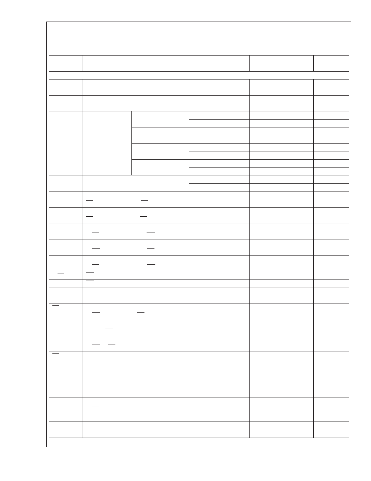
DYNAMIC CONVERTER AND MULTIPLEXER CHARACTERISTICS
−3 dB Unipolar Full V
= 4.85 V
IN
p–p
Power Bandwidth
−3 dB Bipolar Full V
=±4.85V 200 kHz
IN
Power Bandwidth
REFERENCE CHARACTERISTICS (Unipolar Operation V
−
= GND Only)
VREFOut Reference Output Voltage 2.5
∆V
/∆t VREFOut Temperature Coefficient 40 ppm/˚C
REF
∆V
/∆ILLoad Regulation Sourcing 0 mA ≤ IL≤ +4 mA 0.003 0.1 %/mA (Max)
REF
Sinking 0 mA ≥ I
Line Regulation 4.5V ≤ V
I
SC
∆V
t
SU
REF
Short Circuit Current VREFOut = 0V 14 25 mA (Max)
/∆t Long-Term Stability 200 ppm/1 kHr
Start-Up Time CL= 330 µF 20 ms
≥ −1 mA 0.2 0.6 %/mA (Max)
L
+
≤ 5.5V 0.5 6 mV (Max)
DIGITAL AND DC CHARACTERISTICS
V
V
I
I
V
V
I
+I
−I
IN(1)
IN(0)
OUT
IN(1)
IN(0)
OUT(1)
OUT(0)
SC
SC
Logical “1” Input Voltage V+= 5.5V 2.0 V (Min)
Logical “0” Input Voltage V+= 4.5V 0.8 V (Max)
Logical “1” Input Current VIN= 5.0V 0.005 2.5 µA (Max)
Logical “0” Input Current VIN= 0V −0.005 −2.5 µA (Max)
Logical “1” Output Voltage V+= 4.5V:
I
= −360 µA 2.4 V (Min)
OUT
I
= −10 µA 4.25 V (Min)
OUT
Logical “0” Output Voltage V+= 4.5V 0.4 V (Max)
I
= 1.6 mA
OUT
TRI-STATE Output Current V
Output Short Circuit Source Current V
Output Short Circuit V
= 0V −0.01 −3 µA (Max)
OUT
V
= 5V 0.01 3 µA (Max)
OUT
= 0V −40 −10 mA (Min)
OUT
OUT
=DV
+
Sink Current
DI+ Digital Supply Current CS = HIGH
AI
I
I
−
REF
+
Analog Supply Current CS = HIGH 3 4.5 mA (Max)
CS = HIGH, f
Negative Supply Current CS = HIGH 3.5 4.5 mA (Max)
CS = HIGH, f
CS = HIGH, f
Reference Input Current V
+
= 5V 0.7 1.1 mA (Max)
REF
=0Hz 0.15 mA (Max)
CLK
=0Hz 3 mA (Max)
CLK
=0Hz 3.5 mA (Max)
CLK
−
= GND, V−= GND for unipolar
REF
(Note 10)
(Note 11)
200 kHz
±
1% 2.5±2% V (Max)
30 10 mA (Min)
0.75 2 mA (Max)
ADC10154/ADC10158
A
Units
(Limit)
www.national.com5
Electrical Characteristics
The following specifications apply for V+=AV+=DV+= + 5.0 VDC,V
operation or V
=TJ=T
−
= −5.0 VDCfor bipolar operation, and f
MIN
to T
; all other limits TA=TJ= 25˚C. (Note 16)
MAX
= 5.0 MHz unless otherwise specified. Boldface limits apply for T
CLK
+
= 5.000 VDC,V
REF
Symbol Parameter Conditions Typical Limits
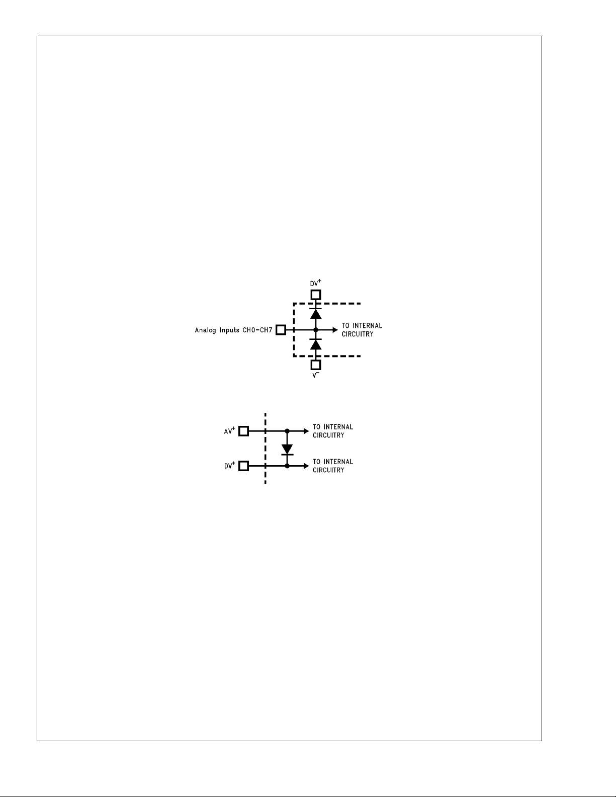
AC CHARACTERISTICS
ADC10154/ADC10158
f
CLK
Clock Frequency 8 5.0 MHz (Max)
Clock Duty Cycle 20 % (Min)
t
C
Conversion 8-Bit Unipolar Mode 16 1/f
Time f
= 5.0 MHz 3.2 µs (Max)
CLK
8-Bit Bipolar Mode 18 1/f
f
= 5.0 MHz 3.6 µs (Max)
CLK
10-Bit Unipolar Mode 20 1/f
f
= 5.0 MHz 4.0 µs (Max)
CLK
10-Bit Bipolar Mode 22 1/f
f
= 5.0 MHz 4.4 µs (Max)
CLK
t
A
t
CR
Acquisition Time 6 1/f
f
= 5.0 MHz 1.2 µs
CLK
Delay between Falling Edge of 0 5 ns (Min)
CS and Falling Edge of RD
t
RC
Delay betwee Rising Edge 0 5 ns (Min)
RD and Rising Edge of CS
t
CW
Delay between Falling Edge 0 5 ns (Min)
of CS and Falling Edge of WR
t
WC
Delay between Rising Edge 0 5 ns (Min)
of WR and Rising Edge of CS
t
RW
Delay between Falling Edge 0 5 ns (Min)
of RD and Falling Edge of WR
t
W(WR)
t
WS
t
DS
t
DH
t
WR
WR Pulse Width 25 50 ns (Min)
WR High to CLK÷2 Low Set-Up Time 5 ns (Max)
Data Set-Up Time 6 15 ns (Max)
Data Hold Time 0 5 ns (Max)
Delay from Rising Edge 0 5 ns (Min)
of WR to Rising Edge RD
t
ACC
Access Time (Delay from Falling CL= 100 pF 25 45 ns (Max)
Edge of RD to Output Data Valid)
tWI,t
RI
Delay from Falling Edge CL= 100 pF 25 40 ns (Max)
of WR or RD to Reset of INT
t
INTL
Delay from Falling Edge of CLK÷2 to
Falling Edge of INT
t
1H,t0H
TRI-STATE Control (Delay from CL= 10 pF, RL=1kΩ 20 35 ns (Max)
Rising Edge of RD to Hi-Z State)
t
RR
Delay between Successive 25 50 ns (Min)
RD Pulses
t
P
Delay between Last Rising Edge
of RD and the Next Falling
Edge of WR
C
IN
C
OUT
Capacitance of Logic Inputs 5 pF
Capacitance of Logic Outputs 5 pF
−
REF
(Note 10)
10 kHz (Min)
40 ns
20 50 ns (Min)
= GND, V−= GND for unipolar
Units
(Note 11)
(Limit)
80 % (Max)
CLK
CLK
CLK
CLK
CLK
A
www.national.com 6
Electrical Characteristics (Continued)
Note 1: Absolute Maximum Ratings indicate limits beyond which damage to the device may occur.
Note 2: Operating Ratings indicateconditionsfor which the device is functional, but do notguaranteespecific performance limits. For guaranteed specifications and
test conditions, see the Electrical Characteristics. The guaranteed specifications apply only for the test conditions listed. Some performance characteristics may
degrade when the device is not operated under the listed test conditions.
Note 3: All voltages are measured with respect to GND, unless otherwise specified.
Note 4: When the input voltage (V
20 mA maximum package input current rating limits the number of pins that can safely exceed the power supplies with an input current of 5 mA to four.
) at any pin exceeds the power supplies (V
IN
<
IN
Note 5: The maximum power dissipation must be derated at elevated temperatures and is dictated by T
allowable power dissipation at any temperature is P
= 150˚C. The typical thermal resistance (θJA) of these parts when board mounted follow:ADC10154 with BIN and CIN suffixes 65˚C/W,ADC10154 with BIJ,
T
Jmax
CIJ and CMJ suffixes 49˚C/W,ADC10154with BIWM and CIWM suffixes 72˚C/W,ADC10158with BIN and CIN suffixes 59˚C/W,ADC10158 with BIJ, CIJ, and CMJ
D
=(T
)/θJAor the number given in the Absolute Maximum Ratings, whichever is lower. For this device,
Jmax−TA
suffixes 46˚C/W, ADC10158 with BIWM and CIWM suffixes 68˚C/W.
Note 6: Human body model, 100 pF capacitor discharged through a 1.5 kΩ resistor.
Note 7: See AN-450 “Surface Mounting Methods and Their Effect on Product Reliability” or the section titled “Surface Mount” found in any post-1986 National
Semiconductor Linear Data Book for other methods of soldering surface mount devices.
Note 8: Two on-chip diodes are tied to each analog input as shown below. They will forward-conduct for analog input voltages one diode drop below V
one diode drop greater than V
+
supply. Be careful during testing at low V+levels (4.5V), as high level analog inputs (5V) can cause an input diode to conduct,
especially at elevated temperatures, whichwill cause errors for analog inputsnear full-scale. The specification allows 50 mV forward bias of either diode;this means
that as long as the analog V
channel will corrupt the reading of a selected channel. This means that if AV
±
4.55 VDC.
≤
does not exceed the supply voltage by more than 50 mV, the output code will be correct. Exceeding this range on an unselected
IN
+
and DV+are minimum (4.5 VDC) and V−is a maximum (−4.5 VDC) full scale must be
V−or V
>
AV+or DV+), the current at that pin should be limited to 5 mA.The
IN
, θJAand the ambient temperature, TA. The maximum
Jmax
−
supply or
ADC10154/ADC10158
DS011225-4
Note 9: A diode exists between AV
+
and DV+as shown below.
DS011225-5
To guarantee accuracy, it is required that the AV+and DV+be connected together to a power supply with separate bypass filter at each V+pin.
Note 10: Typicals are at T
= 25˚C and represent most likely parametric norm.
J=TA
Note 11: Tested limits are guaranteed to National’s AOQL (Average Outgoing Quality Level).
Note 12: One LSB is referenced to 10 bits of resolution.
Note 13: Total unadjusted error includes offset, full-scale, linearity, multiplexer, and hold step errors.
Note 14: For DC Common Mode Error the only specification that is measured is offset error.
Note 15: Channel leakage current is measured after the channel selection.
Note 16: All the timing specifications are tested at the TTL logic levels, V
= 0.8V for a falling edge and VIH= 2.0V for a rising.
IL
www.national.com7
 Loading...