

Page 1
National Semiconductor
Rev 1.3
May 9, 2005
Evaluation Board User’s Guide
ADC10040 10-Bit, 40 MSPS, 3 Volt, 55.5 mW A/D Converter
ADC10065 10-Bit, 65 MSPS, 3 Volt, 68.5 mW A/D Converter
ADC10080 10-Bit, 80 MSPS, 3 Volt, 78.6 mW A/D Converter
© 2005 National Semiconductor Corporation.
1 http://www.national.com
Page 2

Table of Contents
1.0 Introduction
2.0 Quick Start
3.0 Functional Description
4.0 Obtaining Best Results
............................................................................................................................................ 3
............................................................................................................................................. 3
............................................................................................................................. 3
3.1 The Signal Input
3.2 Digital Data Output.
3.3 ADC10080 Control Pins.
3.3.1 The Standby (STBY) Pin
3.3.2 The Data Format (DF) pin
3.3.3 The Input Range Select (IRS) Pin
3.3.4 Power Supply Connections
4.1 Clock Timing
4.2 Coherent Sampling
4.3 FFT Windowing Technique
....................................................................................................................... 3
............................................................................................................................. 4
........................................................................................................................... 4
.................................................................................................................... 4
5.0 Hardware Documentation
.................................................................................................................. 3
........................................................................................................... 3
..................................................................................... 3
.................................................................................... 3
............................................................................... 4
........................................................................................................... 4
....................................................................................................... 4
............................................................................................................... 6
2 http://www.national.com
Page 3

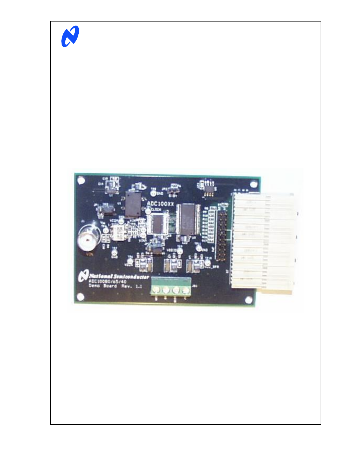
1.0 Introduction
The ADC10080EVAL Design Kit (consisting of the Evaluation Board
and this manual) is designed to ease evaluation and design-in of
National's ADC10040, ADC10065, or ADC10080 10-bit Analog-toDigital Converters, which operate at speeds up to 40, 65, and 80
MSPS. Further reference in this manual to the ADC10080 is meant
to also include the ADC10040 and the ADC10065 unless otherwise
specified. The latest datasheet for these products can be obtained
from http://www.national.com.
The evaluation board can be used in either of two modes. In the
Manual mode, suitable test equipment, such as a logic analyzer,
can be used with the board to evaluate the ADC10080 performance.
In the Computer mode, evaluation is simplified by connecting the
board to the WaveVision™ Digital Interface Board (order number
WAVEVSN BRD 4.0). It is connected to a personal computer
through a USB port and running WaveVision™ software, operating
under Microsoft Windows 95 or later. The WaveVision™ software
can perform an FFT on the captured data upon command and, with
the frequency domain plot, shows dynamic performance in the form
of SNR, SINAD, THD and SFDR.
The signal at J1, the Analog Input to the board, is digitized and is
available at pins B4 through B13 of J2 and pins 10 through 19 of
JP4. See the board schematic for more details.
2.0 Quick Start
Refer to the board layout for locations of test points and major
components.
For Stand-Alone
operation:
1. Select the input voltage range by inserting a jumper into JP1.
Set the jumper on pins 1&2 for 2.0 Vpp. Set the jumper on pins
2&3 for 1.5 Vpp. If no jumper is inserted, 1.0 Vpp is assumed.
2. To make the ADC10080 active, insure there is no jumper on
JP3.
3. Select the output data format using JP2. When the jumper is
on pins 1&2, 2’s complement data format is selected. If the
jumper is on pins 2&3, offset binary is selected.
4. Connect a clean power supply to Power Connector JS1. Refer
to Table 1 for power supply description and requirements.
5. Connect a signal of the selected amplitude (see step 1) from a
50-Ohm source to Analog Input BNC J1. Insure that the signal
is not over-ranged, by examining a histogram. (Either by using
WaveVision
tm
, or the logic analyzer being used.) Over-range
signals will dramatically increase the THD.
6. The digitized signal is available at pins B4 through B13 of J2
and pins 10 through 19 of JP4.
JS1 pin
number
1 Vcc for Crystal and
Description Voltage
Range
2.7 - 3.3 V
VDDA for
ADC10080
2 Ground 0V
3 VDDIO 2.5 – 3.3 V
4 Output Buffer VCC 4.9 – 5.1 V
Table 1
For Computer mode
operation:
tm
1. Connect the evaluation board to the WaveVision
Interface Board. See the instruction manual supplied with the
WaveVision
tm
kit. The latest WaveVisiontm software can be
Digital
obtained from http://www.national.com.
2. Select the input voltage range by inserting a jumper into JP1.
Set the jumper on pins 1&2 for 2.0 Vpp. Set the jumper on pins
2&3 for 1.5 Vpp. If no jumper is inserted, 1.0 Vpp is assumed.
3. To make the ADC10080 active, insure there is no jumper on
JP3.
4. Select pins 2&3 on JP2 so that the output data is offset binary.
5. Connect a clean power supply to Power Connector JS1. Refer
to Table 1 for power supply description and requirements.
6. If the output level goes over range as seen on the data
captured through WaveVision™, reduce the output level from
the signal generator and capture data again. If the output level
does not reach codes of 25 and 1000, increase the output level
from the signal generator and capture data again.
3.0 Functional Description
The ADC10080 Evaluation Board schematic is shown in Section 5.
3.1 The Signal Input
The signal transformer T1 provides single-ended to differential
conversion. The common mode voltage VCOM provided by the
chip, sets the common mode of the input signal by biasing the
center tap of T1.
The differential signal present on the secondary side of the
transformer is then sent through a low pass filter set up by R1, R5 &
C9.
It is important when evaluating the dynamic performance of the
ADC10080 (or any A/D converter), that a clean sine wave be
presented to the converter. To do this it is necessary to use a
bandpass or a low pass filter between the signal source and the
ADC10080 evaluation board input J1. Even the best signal
generators available do not provide adequate noise and distortion
performance for proper evaluation of a 10-bit ADC. A high-quality
bandpass filter with better than 12-bit equivalent noise
characteristics and at least 80dB stop band attenuation is ideal. No
scope or other test equipment should be connected to any input
circuitry while gathering data.
3.2 Digital Data Output.
The digital output data from the ADC10080 is available at the 96-pin
Euro connector J2 and header JP4. Series resistors R7 – R17
provide data line dampening that may occur with long cables. U3
provides buffering to drive the cable. U3’s VCC may be adjusted for
various output levels. Refer to Table 1 for voltage range.
3.3 ADC10080 Control Pins.
The ADC10080 has three control pins, making it a very versatile
converter. They are Standby (Pin 28 – STBY), Data Format (Pin 15
– DF) and Input Range Select (Pin 5 – IRS).
3.3.1 The Standby (STBY) Pin
When this pin is pulled high (pins 1&2 of JP3 are connected), the
converter is put into ‘standby’ mode. The converter consumes only
13.5 mW of power. When STBY is tied to VSSA (JP3 is open), the
ADC is in full operation.
3.3.2 The Data Format (DF) pin
This pin sets the output data format of the ADC10080. When this
pin is pulled to VDDA (pins 1&2 of JP2 are connected), the output is
2’s complement. When pulled down to VSSA (pins 2&3 of JP2 are
connected), the data output is offset binary.
3 http://www.national.com
Page 4
3.3.3 The Input Range Select (IRS) Pin
This pin has three states which the following table summarizes:
JP1 Jumper
setting
IRS State
Input Voltage
Range
(differential)
Pins 1&2 VDDA 2Vpp
Pins 3&4 VSSA 1.5Vpp
Open Floating 1.0Vpp
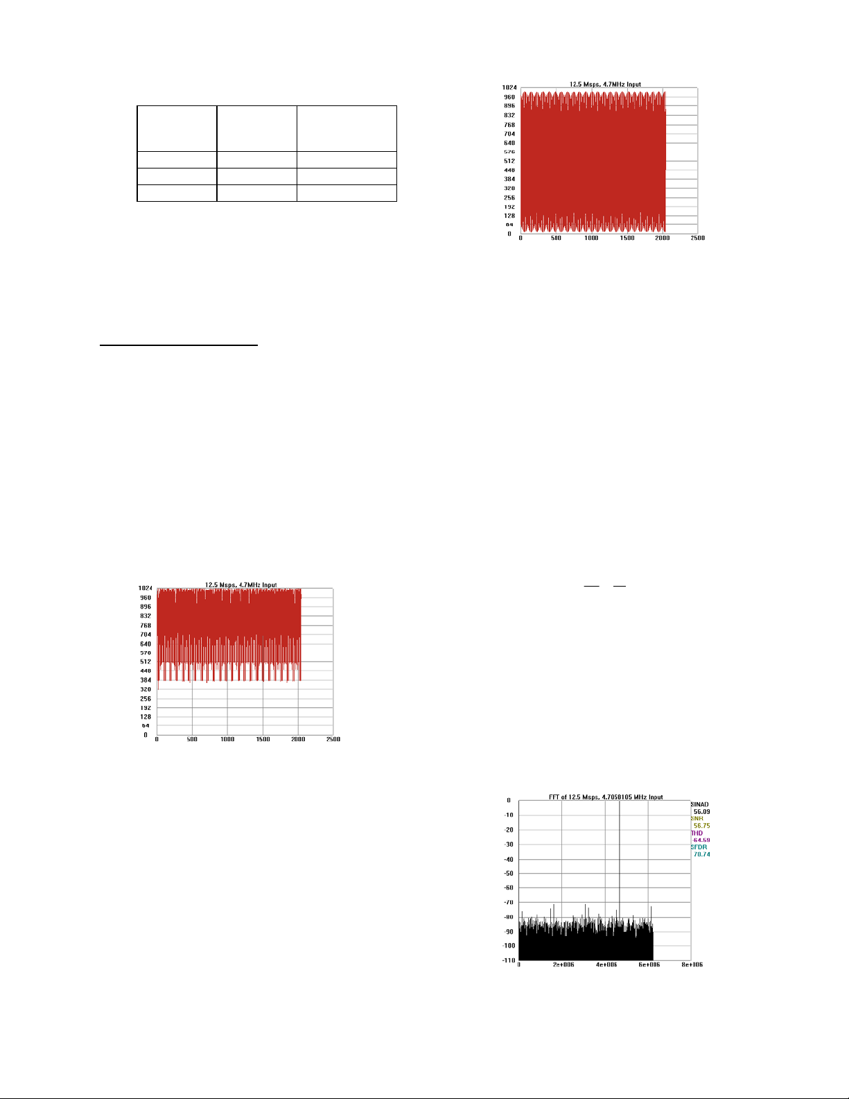
Figure 3. A good data capture of a 4.7MHz input
3.3.4 Power Supply Connections
Power to this board is supplied through power connector JS1. Table
1 describes the pin out, and the allowed voltage ranges
signal at 12.5Msps
4.2 Coherent Sampling
4.0 Obtaining Best Results
Many factors go into reasonable data capture when evaluating an
ADC. These include, but are not limited to, such things as PCB
layout, clock timing, the ratio between the input frequency and
sample rate and the FFT windowing technique.
Here we include very brief discussions on clock timing adjustments
as it relates to the ADC10080 and of sampling and FFT windowing.
4.1 Clock Timing
Because of differing delays in the clock signal and the data from the
ADC, at some sample rates the data from the ADC may be latched
as it is changing, leading to corrupted data, one example of which is
seen in Figure 2, which shows the poor data capture of a 4.7MHz
signal at 12.5Msps that results from poor timing of the clock and
external latch signals relative to each other.
Figure 2. Bad data capture of a 4.7MHz input signal at
12.5Msps due to attempted capture at data transition.
Figure 3 shows a successful data capture of a 4.7MHz input signal
at 12.5Msps with a shorting jumper on JS1.
4 http://www.national.com
Artifacts can result when we perform an FFT on a digitized
waveform, producing inconsistent results when performing repeated
testing. The presence of these artifacts means that the ADC under
test may perform better than the measurements would indicate.
We can eliminate the need for windowing and get more consistent
results if we observe the proper ratios between the input and
sampling frequencies. This greatly increases the spectral resolution
of the FFT, allowing us to more accurately evaluate the spectral
response of the A/D converter. When we do this, however, we must
be sure that the input signal has high spectral purity and stability
and that the sampling clock signal is extremely stable with minimal
jitter.
Coherent sampling of a periodic waveform occurs when a prime
integer number of cycles exists in the sample window. The
relationship between the number of cycles sampled (CY), the
number of samples taken (SS), the signal input frequency (fin) and
the sample rate (fs), for coherent sampling, is
f
CY
in
=
f
SS
s
CY, the number of cycles in the data record, must be a prime
integer number and SS, the number of samples in the data record,
must be a factor of 2 integer.
Further, fin (signal input frequency) and fs (sampling rate) should be
locked to each other. If these frequencies are locked to each other,
whatever frequency instability (jitter) is present in one of the signal
is present in the other signal and these jitter terms will cancel each
other.
Windowing (an FFT Option under WaveVision™) should be turned
off for coherent sampling. The results of coherent sampling can be
seen in the FFT plot seen in Figure 4. Note how narrow is the bin
(how fine are the lines) in this plot as compared with the plots of
Figures 5 through 7.
Figure 4. Coherent sampling will indicate accurate
dynamic performance of the ADC
4.3 FFT Windowing Technique
Page 5

The FFT assumes the waveform being evaluated is repetitive and
that it extends from -∞ to +∞ in time. In order to make the evaluated
signal appear as though it extends from -∞ to +∞, FFT algorithms
fold the signal such that the last point in the data record is followed
by the first point. To the extent that this is true, there will be no
discontinuities in the folded waveform.
However, folded waveforms often have a discontinuity and this
leads to erroneous dynamic performance measurements. This is
shown in Figure 5, where we see poor, inaccurate dynamic
performance measurements at the upper right corner, as well as a
spreading around the input frequency. This spreading is called
"leakage".
Figure 5. A discontinuity in the folded finite-time
waveform leads to misleading results in the FFT.
There are many windowing techniques in use today to minimize this
problem. Figure 6 shows an FFT plot of the same data used in
Figure 5, but using the Hanning windowing function. Note the
improved dynamic performance over no windowing as in Figure 5.
The Flat-Top windowing function even yields similar dynamic
performance measurements, as can be seen in Figure 7. Compare
the dynamic performance parameters of Figures 6 and 7 with those
of coherent sampling (Figure 4).
Figure 7. The Flat-Top windowing function yields
slightly improved dynamic performance
measurements over the Hanning function.
Figure 6. Windowing will reduce the effects of
waveform folding. The Hanning windowing function is
used here.
5 http://www.national.com
Page 6

5.0 Hardware Documentation
Please see the attached pages for a board layout, hardware schematic, and Bill of Materials.
6 http://www.national.com
Page 7

7 http://www.national.com
Page 8

ADC10xxx Eval. Board Revised: Wednesday, March 03, 2004
Revision: 1.1
National Semiconductor
Bill Of Materials
Item Qty Reference Part
1 10 C1,C7,C15,C18,C19,C20, .1uF
C21,C24,C26,C29
2 6 C2,C14,C22,C23,C25,C28 10uF
3 2 C8,C3 4.7uF
4 8 C4,C5,C6,C11,C12,C13,C16, .1uF
C17
5 1 C9 68pf
6 1 C10 100pf
7 1 C27 0.1uF
8 2 JP1,JP2 HEADER 3
9 1 JP3 HEADER 2
10 1 JP4 Logic Analyzer
11 1 JS1 CONN TRBLK 4
12 1 J1 Vert. PCB mount
13 1 J2 FUTUREBUS_96
14 4 L1,L2,L3,L4 EXC-CET103U
15 4 R1,R5 24.9
16 1 R4 49.9
17 1 R6 100K
18 11 R7,R8,R9,R10,R11,R12,R13, 49.9
R14,R15,R16,R17
19 1 TP1 CLOCK
20 1 TP2 VIN21 1 TP3 VCOM
22 1 TP4 VIN
23 1 TP5 VIN+
24 1 TP6 VDDA
25 2 TP7,TP8 GND
26 1 TP9 VDDIO
27 1 TP10 VCC_Bfr
28 1 T1 TRANSFORMER CT
29 1 U1 Oscillator/sm4
30 1 U2 ADC10080
31 1 U3 74ACTQ16244/SO
32 1 U4 24C02/SO8
33 2 R2,R3 NP
8 http://www.national.com
Page 9

BY USING THIS PRODUCT, YOU ARE AGREEING TO BE BOUND BY THE TERMS AND CONDITIONS OF NATIONAL
SEMICONDUCTOR'S END USER LICENSE AGREEMENT. DO NOT USE THIS PRODUCT UNTIL YOU HAVE READ AND AGREED
TO THE TERMS AND CONDITIONS OF THAT AGREEMENT. IF YOU DO NOT AGREE WITH THEM, CONTACT THE VENDOR
WITHIN TEN (10) DAYS OF RECEIPT FOR INSTRUCTIONS ON RETURN OF THE UNUSED PRODUCT FOR A REFUND OF THE
PURCHASE PRICE PAID, IF ANY.
The ADC10040, ADC10065, and ADC10080 Evaluation Boards are intended for product evaluation purposes only and are not intended
for resale to end consumers, is not authorized for such use and is not designed for compliance with European EMC Directive
89/336/EEC, or for compliance with any other electromagnetic compatibility requirements.
National Semiconductor Corporation does not assume any responsibility for use of any circuitry or software supplied or described. No
circuit patent licenses are implied.
LIFE SUPPORT POLICY
NATIONAL'S PRODUCTS ARE NOT AUTHORIZED FOR USE AS CRITICAL COMPONENTS IN LIFE SUPPORT DEVICES OR
SYSTEMS WITHOUT THE EXPRESS WRITTEN APPROVAL OF THE PRESIDENT OF NATIONAL SEMICONDUCTOR
CORPORATION. As used herein:
1. Life support devices or systems are devices or systems
which, (a) are intended for surgical implant into the body,
or (b) support or sustain life, and whose failure to perform,
when properly used in accordance with instructions for use
2. A critical component is any component in a life support
device or system whose failure to perform can be
reasonably expected to cause the failure of the life support
device or system, or to affect its safety or effectiveness.
provided in the labeling, can be reasonably expected to
result in a significant injury to the user.
National Semiconductor Corporation
Americas
Tel: 1-800-272-9959
Fax: 1-800-737-7018
Email: support@nsc.com
www.national.com
National does not assume any responsibility for any circuitry described, no
circuit patent licenses are implied and National reserves the right at any
time without notice to change said circuitry and specifications.
National Semiconductor Europe
Fax: +49 (0) 1 80-530 85 86
Email: europe.support@nsc.com
Deutsch Tel: +49 (0) 699508 6208
English Tel: +49 (0) 870 24 0 2171
Français Tel: +49 (0) 141 91 8790
National Semiconductor
Asia Pacific Customer
Response Group
Tel: 65-2544466
Fax: 65-2504466
Email:sea.support@nsc.com
National Semiconductor
Japan Ltd.
Tel: 81-3-5639-7560
Fax: 81-3-5639-7507
9 http://www.national.com
Page 10

IMPORTANT NOTICE
Texas Instruments Incorporated and its subsidiaries (TI) reserve the right to make corrections, modifications, enhancements, improvements,
and other changes to its products and services at any time and to discontinue any product or service without notice. Customers should
obtain the latest relevant information before placing orders and should verify that such information is current and complete. All products are
sold subject to TI’s terms and conditions of sale supplied at the time of order acknowledgment.
TI warrants performance of its hardware products to the specifications applicable at the time of sale in accordance with TI’s standard
warranty. Testing and other quality control techniques are used to the extent TI deems necessary to support this warranty. Except where
mandated by government requirements, testing of all parameters of each product is not necessarily performed.
TI assumes no liability for applications assistance or customer product design. Customers are responsible for their products and
applications using TI components. To minimize the risks associated with customer products and applications, customers should provide
adequate design and operating safeguards.
TI does not warrant or represent that any license, either express or implied, is granted under any TI patent right, copyright, mask work right,
or other TI intellectual property right relating to any combination, machine, or process in which TI products or services are used. Information
published by TI regarding third-party products or services does not constitute a license from TI to use such products or services or a
warranty or endorsement thereof. Use of such information may require a license from a third party under the patents or other intellectual
property of the third party, or a license from TI under the patents or other intellectual property of TI.
Reproduction of TI information in TI data books or data sheets is permissible only if reproduction is without alteration and is accompanied
by all associated warranties, conditions, limitations, and notices. Reproduction of this information with alteration is an unfair and deceptive
business practice. TI is not responsible or liable for such altered documentation. Information of third parties may be subject to additional
restrictions.
Resale of TI products or services with statements different from or beyond the parameters stated by TI for that product or service voids all
express and any implied warranties for the associated TI product or service and is an unfair and deceptive business practice. TI is not
responsible or liable for any such statements.
TI products are not authorized for use in safety-critical applications (such as life support) where a failure of the TI product would reasonably
be expected to cause severe personal injury or death, unless officers of the parties have executed an agreement specifically governing
such use. Buyers represent that they have all necessary expertise in the safety and regulatory ramifications of their applications, and
acknowledge and agree that they are solely responsible for all legal, regulatory and safety-related requirements concerning their products
and any use of TI products in such safety-critical applications, notwithstanding any applications-related information or support that may be
provided by TI. Further, Buyers must fully indemnify TI and its representatives against any damages arising out of the use of TI products in
such safety-critical applications.
TI products are neither designed nor intended for use in military/aerospace applications or environments unless the TI products are
specifically designated by TI as military-grade or "enhanced plastic." Only products designated by TI as military-grade meet military
specifications. Buyers acknowledge and agree that any such use of TI products which TI has not designated as military-grade is solely at
the Buyer's risk, and that they are solely responsible for compliance with all legal and regulatory requirements in connection with such use.
TI products are neither designed nor intended for use in automotive applications or environments unless the specific TI products are
designated by TI as compliant with ISO/TS 16949 requirements. Buyers acknowledge and agree that, if they use any non-designated
products in automotive applications, TI will not be responsible for any failure to meet such requirements.
Following are URLs where you can obtain information on other Texas Instruments products and application solutions:
Products Applications
Audio www.ti.com/audio Automotive and Transportation www.ti.com/automotive
Amplifiers amplifier.ti.com Communications and Telecom www.ti.com/communications
Data Converters dataconverter.ti.com Computers and Peripherals www.ti.com/computers
DLP® Products www.dlp.com Consumer Electronics www.ti.com/consumer-apps
DSP dsp.ti.com Energy and Lighting www.ti.com/energy
Clocks and Timers www.ti.com/clocks Industrial www.ti.com/industrial
Interface interface.ti.com Medical www.ti.com/medical
Logic logic.ti.com Security www.ti.com/security
Power Mgmt power.ti.com Space, Avionics and Defense www.ti.com/space-avionics-defense
Microcontrollers microcontroller.ti.com Video and Imaging www.ti.com/video
RFID www.ti-rfid.com
OMAP Mobile Processors www.ti.com/omap
Wireless Connectivity www.ti.com/wirelessconnectivity
TI E2E Community Home Page e2e.ti.com
Mailing Address: Texas Instruments, Post Office Box 655303, Dallas, Texas 75265
Copyright © 2012, Texas Instruments Incorporated
Page 11

Mouser Electronics
Authorized Distributor
Click to View Pricing, Inventory, Delivery & Lifecycle Information:
Texas Instruments:
ADC10080EVAL
 Loading...