

Page 1

DAQ
DAQ-STC™ Technical Reference Manual
System Timing Controller for Data Acquisition
DAQ-STC Technical Reference Manual
January 1999 Edition
Part Number 340934B-01
Page 2

Internet Support
E-mail: support@natinst.com
FTP Site: ftp.natinst.com
Web Address: http://www.natinst.com
Bulletin Board Support
BBS United States: 512 794 5422
BBS United Kingdom: 01635 551422
BBS France: 01 48 65 15 59
Fax-on-Demand Support
512 418 1111
Telephone Support (USA)
Tel: 512 795 8248
Fax: 512 794 5678
International Offices
Australia 03 9879 5166, Austria 0662 45 79 90 0, Belgium 02 757 00 20, Brazil 011 288 3336,
Canada (Ontario) 905 785 0085, Canada (Québec) 514 694 8521, Denmark 45 76 26 00, Finland 09 725 725 11,
France 01 48 14 24 24, Germany 089 741 31 30, Hong Kong 2645 3186, Israel 03 6120092, Italy 02 413091,
Japan 03 5472 2970, Korea 02 596 7456, Mexico 5 520 2635, Netherlands 0348 433466, Norway 32 84 84 00,
Singapore 2265886, Spain 91 640 0085, Sweden 08 730 49 70, Switzerland 056 200 51 51, Taiwan 02 377 1200,
United Kingdom 01635 523545
National Instruments Corporate Headquarters
6504 Bridge Point Parkway Austin, Texas 78730-5039 USA Tel: 512 794 0100
© Copyright 1995, 1998 National Instruments Corporation. All rights reserved.
Page 3

Important Information
Warranty
The DAQ-STC is warranted against defects in materials and workmanship for a period of one year from the date of
shipment, as evidenced by receipts or other documentation. National Instruments will, at its option, repair or replace
equipment that proves to be defect ive du ring t he wa rranty period . Th is warranty incl udes parts a nd l abor.
The media on which you receive National Instruments software are warranted not to fail to execute programming
instructions, due to defects in materials and work man ship, for a peri od of 90 d ays from da te o f sh ipm ent, as evi denced
by receipts or other documentation. National Instruments will, at its option, repair or replace software media that do not
execute programming instructions if National Instruments receives noti ce of su ch defect s d uring th e warranty perio d.
National Instruments does not warrant that the op eration of t he soft ware shall b e uni nterrup ted or erro r free.
A Return Material Authorization (RMA) number must b e ob tain ed fro m th e facto ry an d clearl y mark ed on t he outsi de
of the package before any equipment wil l be accepted for warranty work. National Instruments will pay the shippi ng costs
of returning to the owner parts which are covered by warran ty.
National Instruments believes that the information in this document is accurate. The document has been carefully
reviewed for technical accuracy. In the event that technical or typographical errors exist, National Instruments reserves
the right to make changes to subsequent editions of this document without prior notice to holders of this edition. The
reader should consult National Instruments if errors are suspected. In no event shall National Instruments be liable for
any damages arising out of or related to th is d ocum ent o r th e in form ation con tained in i t.
XCEPT AS SPECIFIED HEREIN
E
ANY WARRANTY OF MERCHANTABILITY OR FITNESS FOR A PARTICULAR PURPOSE
BY FAULT OR NEGLIGENCE ON THE PART OF NATIONAL INSTRUMENTS SHALL BE LIMITED TO THE AMOUNT THERETOFORE PAID BY THE
CUSTOMER
OR INCIDENTAL OR CONSEQUENTIAL DAMAGES, EVEN IF ADVISED OF THE POSSIBILITY THEREOF
National Instruments will apply regardless of the form of action, wh ether in con tract or tort , incl udin g n egli gen ce.
Any action against National Instruments must be brought within one year after the cause of action accrues. National
Instruments shall not be liable for any delay in performance due to causes beyond its reasonable control. The warranty
provided herein does not cover damages, defects, malfuncti ons, or s ervice failur es caused by own er’s fai lure to fol low
the National Instruments installation, operation, or maintenance instructions; owner’s modification of the product;
owner’s abuse, misuse, or negligent acts; and power failure or surges, fire, flood, accident, actions of third parties,
or other events outside reasonable control.
ATIONAL INSTRUMENTS WILL NOT BE LIABLE FOR DAMAGES RESULTING FROM LOSS OF DATA, PROFITS, USE OF PRODUCTS
. N
ATIONAL INSTRUMENTS MAKES NO WARRANTIES, EXPRESS OR IMPLIED, AND SPECIFICALLY DISCLAIMS
, N
Copyright
Under the copyright laws, this publication may not be reproduced or transmitted in any form, electronic or mechanical,
including photocopying, recording, storing in an information retrieval system, or translating, in whole or in part, without
the prior written consent of National Instruments Corporation.
USTOMER’S RIGHT TO RECOVER DAMAGES CAUSED
. C
. This limitation of the liability of
,
Trademarks
CVI™, DAQ-STC™, NI-DAQ™, and RTSI™ are trademarks of National Instruments Corporation.
Product and company names mentioned herein are trademarks or trade names of their respective companies.
WARNING REGARDING MEDICAL AND CLINICAL USE OF NATIONAL INSTRUMENTS PRODUCTS
National Instruments products are not designed with com ponent s and tes ting inten ded to ensure a l evel of reliab ilit y
suitable for use in treatment and diagnosis of humans. Applications of National Instruments products invol ving m edical
or clinical treatment can create a potential for accidental injury caused by product failure, or by errors on the part of the
user or application designer. Any use or application of National Instruments products for or involving medical or clinical
treatment must be performed by properly trained and qualified medical personnel, and all traditional medical safeguards,
equipment, and procedures that are appropriate in the particular situation to prevent serious injury or death should always
continue to be used when National Instruments products are being used . National Instrum ents product s are NOT intended
to be a substitute for any form of established process, procedure, or equipment used to monitor or safeguard human health
and safety in medical or clinical treatment.
Page 4

Contents
About This Manual
Organization of This Manual.........................................................................................xxiii
Conventions Used in This Manual.................................................................................xxv
National Instruments Documentation.......................................................................... ..xxvi
Related Documentation........................................... .......................................................xxvi
Customer Communication........................................................................ .....................xxvii
Chapter 1
Introduction
1.1 DAQ-STC Applications......................................... ............................................1-2
1.1.1 Analog Input Application...................................................................1-2
1.1.2 Analog Output Application ................................................................1-3
1.2 DAQ-STC Block Diagram.................................................................................1-4
Chapter 2
Analog Input Timing/Control
2.1 Overview............................................................................................................2-1
2.1.1 Programming the AITM.....................................................................2-1
2.2 Features ..............................................................................................................2-2
2.3 Simplified Model................................................................................................2-4
2.4 Analog Input Functions......................................................................................2-6
2.4.1 Low-Level Timing and Control..........................................................2-6
2.4.1.1 ADC Control................................... ..............................2-7
2.4.1.2 Data FIFO Control........................................................2-7
2.4.1.3 Configuration FIFO and External
2.4.1.4 CONVERT Timing.......................................................2-9
2.4.2 Scan-Level Timing and Control.........................................................2-11
2.4.2.1 Internal START Mode..................................................2-11
2.4.2.2 External START Mode.................................................2-12
2.4.3 Acquisition-Level Timing and Control..............................................2-14
2.4.3.1 Posttrigger Acquisition Mode.......................................2-14
2.4.3.2 Pretrigger Acquisition Mode ........................................2-14
2.4.3.3 Continuous Acquisition Mode......................................2-15
2.4.3.4 Staged Acquisition........................................................2-16
2.4.3.5 Master/Slave Trigger ....................................................2-16
2.4.4 Gating.................................................................................................2-16
2.4.4.1 Free-Run Gating Mode.................................................2-17
Multiplexer Control ................................................... 2-7
©
National Instruments Corporation v DAQ-STC Technical Reference Manual
Page 5

Contents
2.4.4.2 Halt-Gating Mode................................................ .........2-17
2.4.5 Single-Wire Mode..............................................................................2-18
2.5 Pin Locator Interface..........................................................................................2-19
2.6 Programming Information .................................................................................2-24
2.6.1 Register and Bitfield Programming Considerations .......................... 2-24
2.6.2 Windowing Registers.........................................................................2-25
2.6.3 Programming for an Analog Input Operation....................................2-25
2.6.3.1 Resetting.......................................................................2-26
2.6.3.2 Board Power-up Initialization ......................................2-27
2.6.3.3 Initialize Configuration Memory Output......................2-28
2.6.3.4 Board Environment Setup ............................................2-29
2.6.3.5 FIFO Request................................................................2-30
2.6.3.6 Hardware Gate Programming.......................................2-30
2.6.3.7 Software Gate Operation..............................................2-31
2.6.3.8 Trigger Signals .............................................................2-32
2.6.3.9 Number of Scans ..........................................................2-33
2.6.3.10 Start of Scan .................................................................2-34
2.6.3.11 End of Scan...................................................................2-37
2.6.3.12 Convert Signal..................................................... .........2-38
2.6.3.13 Enable Interrupts ..........................................................2-40
2.6.3.14 Arming..........................................................................2-41
2.6.3.15 Starting the Acquisition................................................2-41
2.6.3.16 Analog Input Program..................................................2-42
2.6.4 Single Scan.................................................... .....................................2-42
2.6.5 Change Scan Rate during an Acquisition ..........................................2-43
2.6.6 Staged Acquisition.............................................................................2-44
2.6.7 Master/Slave Operation Considerations.............................................2-45
2.6.8 Analog Input-Related Interrupts ........................................................2-46
2.6.9 Bitfield Descriptions ..........................................................................2-48
2.7 Timing Diagrams...............................................................................................2-84
2.7.1 Signal Definitions ...................................... ..................................... ...2-84
2.7.1.1 CONVERT_SRC............................................ ..............2-84
2.7.1.2 OUT_CLK....................................................................2-85
2.7.2 Basic Analog Input Timing................................................................2-86
2.7.3 Data FIFOs.........................................................................................2-88
2.7.4 Configuration Memory ......................................................................2-89
2.7.5 Maximum Rate Analog Input ............................................................2-91
2.7.6 External CONVERT Source..............................................................2-92
2.7.7 External Triggers................................................................................2-93
2.7.8 Trigger Output....................................................................................2-97
2.7.8.1 START1 and START2 Triggers ..................................2-97
2.7.8.2 START Trigger and SCAN_IN_PROG Assertion....... 2-100
DAQ-STC Technical Reference Manual vi
©
National Instruments Corporation
Page 6

Contents
2.7.8.3 SCAN_IN_PROG Deassertion.....................................2-103
2.7.8.4 STOP Trigger................................................................ 2-103
2.7.9 Counter Outputs................................... ..................................... ..........2-105
2.7.9.1 SC_TC ......................................... .................................2-105
2.7.9.2 SI_TC........................................................................ ....2-105
2.7.9.3 DIV_TC ........................................................................2-106
2.7.10 Macro-Level Analog Input Timing ....................................................2-106
2.7.11 External Gating...................................................................................2-109
2.8 Detailed Description...........................................................................................2-112
2.8.1 Internal Signals and Operation...........................................................2-113
2.8.2 Trigger Selection and Conditioning ...................................................2-119
2.8.2.1 Using Edge Detection...................................................2-122
2.8.2.2 Using Synchronization..................................................2-122
2.8.2.3 Trigger Signals..............................................................2-122
2.8.3 Analog Input Counters .......................................................................2-123
2.8.3.1 SC Counter....................................................... .............2-124
2.8.3.2 SC Control ................................................................ ....2-124
2.8.3.3 SI Counter.....................................................................2-126
2.8.3.4 SI Control......................................................................2-126
2.8.3.5 SI2 Counter...................................................................2-127
2.8.3.6 SI2 Control....................................................................2-127
2.8.3.7 DIV Counter .................................................................2-128
2.8.3.8 DIV Control..................................................................2-129
2.8.4 Interrupt Control.................................................................................2-130
2.8.5 Error Detection...................................................................................2-132
2.8.5.1 Overrun Error................................................................2-132
2.8.5.2 Overflow Error..............................................................2-132
2.8.5.3 SC_TC Error.................................................................2-132
2.8.6 Nominal Signal Pulsewidths...............................................................2-133
Chapter 3
Analog Output Timing/Control
3.1 Overview............................................................................................................3-1
3.1.1 Programming the AOTM ...................................................................3-2
3.2 Features ..............................................................................................................3-2
3.3 Simplified Model................................................................................................3-4
3.4 Analog Output Functions...................................................................................3-5
3.4.1 Primary Group Analog Output Modes...............................................3-5
3.4.1.1 DAQ-STC-Driven Analog Output................................3-6
3.4.1.2 CPU-Driven Analog Output .........................................3-6
3.4.1.3 DAQ-STC and CPU Conflict .......................................3-7
3.4.2 DAC Interface ..................................... ...............................................3-8
©
National Instruments Corporation vii DAQ-STC Technical Reference Manual
Page 7

Contents
3.4.3 Data Interfaces ...................................................................................3-8
3.4.3.1 FIFO Data Interface......................................................3-8
3.4.3.2 Serial Link Data Interface ............................................3-10
3.4.3.3 Unbuffered Data Interface......................................... ...3-11
3.4.4 Update Timing for Primary Group Analog Output............................3-11
3.4.4.1 Internal UPDATE.........................................................3-11
3.4.4.2 External UPDATE........................................................3-12
3.4.5 Buffer Timing and Control for Primary Analog Output.................... 3-12
3.4.5.1 Single-Buffer Mode ......................................................3-13
3.4.5.2 Continuous Mode .........................................................3-13
3.4.5.3 Waveform Staging........................................................3-14
3.4.5.4 Mute Buffers.................................................................3-15
3.4.5.5 Master/Slave Trigger....................................................3-15
3.4.6 Secondary Analog Output..................................................................3-16
3.5 Pin Interface.......................................................................................................3-16
3.6 Programming Information .................................................................................3-20
3.6.1 Programming for a Primary Analog Output Operation .....................3-20
3.6.1.1 Overview ......................................................................3-21
3.6.1.2 Resetting.......................................................................3-21
3.6.1.3 Board Power-up Initialization ......................................3-22
3.6.1.4 Trigger Signals .............................................................3-23
3.6.1.5 Number of Buffers........................................................3-24
3.6.1.6 Update Selection...........................................................3-26
3.6.1.7 Channel Select..............................................................3-28
3.6.1.8 LDAC Source and UPDATE Mode.............................3-29
3.6.1.9 Stop On Error ...............................................................3-29
3.6.1.10 FIFO Mode...................................................................3-29
3.6.1.11 Enable Interrupts ..........................................................3-30
3.6.1.12 Arming..........................................................................3-30
3.6.1.13 Starting the Waveform .................................................3-31
3.6.1.14 Primary Analog Output Program..................................3-31
3.6.2 Waveform Staging for Primary Analog Output.................................3-32
3.6.3 Changing Update Rate during an Output Operation for
Primary Analog Output Group ........................................................3-34
3.6.4 Master/Slave Operation Considerations for Primary Analog
Output Group ..................................................................................3-35
3.6.5 Primary Analog Output Group-Related Interrupts.............................3-35
3.6.6 Programming for a Secondary Analog Output Group Operation ...... 3-38
3.6.6.1 Overview ......................................................................3-38
3.6.6.2 Resetting.......................................................................3-38
3.6.6.3 Board Power-up Initialization ......................................3-39
3.6.6.4 Hardware Gate Programming.......................................3-39
3.6.6.5 Software Gate Operation..............................................3-40
DAQ-STC Technical Reference Manual viii
©
National Instruments Corporation
Page 8

Contents
3.6.6.6 Counting for Waveform Staging...................................3-40
3.6.6.7 Update Selection...........................................................3-40
3.6.6.8 Arming..........................................................................3-41
3.6.6.9 Secondary Analog Output Program..............................3-41
3.6.7 Waveform Staging for Secondary Analog Output .............................3-42
3.6.8 Changing Update Rate during an Output Operation for
Secondary Analog Output ...............................................................3-44
3.6.9 Master/Slave Operation Considerations for
Secondary Analog Output ...............................................................3-45
3.6.10 Secondary Analog Output-Related Interrupts....................................3-45
3.6.11 Bitfield Descriptions...........................................................................3-45
3.7 Timing Diagrams................................................................................................3-84
3.7.1 Signal Definitions......................................... ......................................3-84
3.7.1.1 UPDATE_SRC.............................................................3-85
3.7.1.1 UI2_SRC....................................................... ................3-85
3.7.1.1 OUT_CLK ....................................................................3-86
3.7.2 DAQ-STC-Driven Analog Output Timing.........................................3-86
3.7.3 CPU-Driven Analog Output Timing ..................................................3-88
3.7.4 DAQ-STC- and CPU-Driven Analog Output Timing........................3-90
3.7.5 Secondary Analog Output Timing......................................................3-93
3.7.6 Decoded Signal Timing......................................................................3-94
3.7.7 Local Buffer Mode Timing ................................................................3-96
3.7.8 Unbuffered Data Interface Timing.....................................................3-98
3.7.9 Maximum Update Rate Timing..........................................................3-101
3.7.10 External Trigger Timing .....................................................................3-102
3.7.11 Trigger Output....................................................................................3-104
3.7.11.1 START1 Trigger................................ ...........................3-104
3.7.12 Counter Outputs................................... ..................................... ..........3-107
3.7.12.1 BC_TC..........................................................................3-107
3.7.12.2 UC_TC................................. ..................................... ....3-108
3.8 Detailed Description...........................................................................................3-108
3.8.1 Internal Signals and Operation...........................................................3-109
3.8.2 Trigger Selection and Conditioning ...................................................3-114
3.8.2.1 Using Edge Detection...................................................3-116
3.8.2.2 Using Synchronization..................................................3-116
3.8.2.3 Trigger Signals..............................................................3-116
3.8.3 Analog Output Counters.....................................................................3-117
3.8.3.1 UI Counter ........................... .........................................3-117
3.8.3.2 UI Control.............................................................. .......3-118
3.8.3.3 UC Counter...................................................................3-118
3.8.3.4 UC Control....................................................................3-119
3.8.3.5 BC Counter ...................................................................3-120
3.8.3.6 BC Control....................................................................3-120
©
National Instruments Corporation ix DAQ-STC Technical Reference Manual
Page 9

Contents
3.8.3.7 UI2 Counter..................................................................3-121
3.8.3.8 UI2 Control...................................................................3-121
3.8.4 Interrupt Control .......................................................................... ......3-122
3.8.5 Error Detection...................................................................................3-122
3.8.5.1 Overrun Error ...............................................................3-122
3.8.5.2 BC_TC Error................................................................3-123
3.8.5.3 BC_TC Trigger Error...................................................3-123
3.8.5.4 UI2_TC Error ...............................................................3-123
3.8.6 Output Control .......................... ..................................... ....................3-123
3.8.7 Nominal Signal Pulsewidths..............................................................3-124
Chapter 4
General-Purpose Counter/Timer
4.1 Overview............................................................................................................4-1
4.1.1 Programming the GPCT.....................................................................4-1
4.2 Features..............................................................................................................4-1
4.3 Simplified Model...............................................................................................4-2
4.4 Counter/Timer Functions...................................................................................4-3
4.4.1 Event Counting ..................................................................................4-3
4.4.1.1 Simple Event Counting.................................................4-4
4.4.1.2 Simple Gated-Event Counting......................................4-4
4.4.1.3 Buffered Noncumulative Event Counting.................... 4-4
4.4.1.4 Buffered Cumulative Event Counting.......................... 4-5
4.4.1.5 Relative Position Sensing.............................................4-6
4.4.2 Time Measurement ............................................................................4-6
4.4.2.1 Single-Period Measurement .........................................4-6
4.4.2.2 Single-Pulsewidth Measurement..................................4-7
4.4.2.3 Buffered Period Measurement......................................4-7
4.4.2.4 Buffered Semiperiod Measurement..............................4-8
4.4.2.5 Buffered Pulsewidth Measurement .............................. 4-9
4.4.3 Pulse Generation ................................................................................4-9
4.4.3.1 Single Pulse Generation ...............................................4-9
4.4.3.2 Single Triggered Pulse Generation...............................4-10
4.4.3.3 Retriggerable Single Pulse Generation.........................4-11
4.4.3.4 Buffered Retriggerable Single Pulse Generation ......... 4-11
4.4.4 Pulse-Train Generation ......................................................................4-12
4.4.4.1 Continuous Pulse-Train Generation.............................4-12
4.4.4.2 Buffered Static Pulse-Train Generation ....................... 4-13
4.4.4.3 Buffered Pulse-Train Generation .................................4-14
4.4.4.4 Frequency Shift Keying (FSK).....................................4-14
4.4.4.5 Pulse Generation for ETS.............................................4-15
4.5 Pin Interface.......................................................................................................4-16
DAQ-STC Technical Reference Manual x
©
National Instruments Corporation
Page 10

Contents
4.6 Programming Information..................................................................................4-17
4.6.1 Programming for a GPCT Operation .................................................4-17
4.6.1.1 Overview.......................................................................4-17
4.6.1.2 Notation ........................................................................4-18
4.6.1.3 Resetting .......................................................................4-18
4.6.1.4 Arming..........................................................................4-18
4.6.1.5 Simple Event Counting.................................................4-19
4.6.1.6 Buffered Event Counting. .............................................4-20
4.6.1.7 Relative Position Sensing ............................................. 4-23
4.6.1.8 Single-Period and Pulsewidth Measurement ................4-24
4.6.1.9 Buffered Period, Semiperiod, and Pulsewidth
Measurement..............................................................4-26
4.6.1.10 Pulse and Continuous Pulse-Train Generation .............4-28
4.6.1.11 Frequency Shift Keying................................................4-31
4.6.1.12 Pulse-Train Generation for ETS ...................................4-33
4.6.1.13 Reading the Counter Contents......................................4-34
4.6.1.14 Reading the Hardware Save Registers..........................4-34
4.6.1.15 Enabling the General Purpose
Counter/Timer Output Pin .........................................4-35
4.6.2 Bitfield Descriptions...........................................................................4-35
4.7 Timing Diagrams................................................................................................4-53
4.7.1 CTRSRC Minimum Period and Minimum Pulsewidth......................4-55
4.7.2 CTRSRC to CTROUT Delay.............................................................4-55
4.7.3 G_GATE Minimum Pulsewidth.........................................................4-56
4.7.4 CTRGATE to CTROUT Delay..........................................................4-57
4.7.5 CTRGATE to INTERRUPT...............................................................4-57
4.7.6 CTRGATE Setup................................................................................4-58
4.7.7 CTR_U/D Setup .................................................................................4-59
4.8 Detailed Description...........................................................................................4-61
4.8.1 Internal Signals and Operation...........................................................4-62
4.8.2 G_SOURCE Selection and Conditioning...........................................4-63
4.8.3 G_GATE Selection and Conditioning................................................4-64
4.8.4 G_UP_DOWN Control ................................... .. .................................4-64
4.8.5 G_OUT Conditioning and Routing ....................................................4-65
4.8.6 G_CONTROL Conditioning..............................................................4-67
4.8.7 Gate Actions.......................................................................................4-67
4.8.7.1 START/STOP on G_CONTROL.................................4-68
4.8.7.2 Save on G_GATE.........................................................4-68
4.8.7.3 Reload on G_CONTROL .............................................4-68
4.8.7.4 UP/DOWN on G_CONTROL......................................4-69
4.8.7.5 Generate Interrupt on G_GATE....................................4-69
4.8.7.6 Change Output Polarity on G_GATE...........................4-69
4.8.7.7 Select Load Register on G_CONTROL .......................4-69
©
National Instruments Corporation xi DAQ-STC Technical Reference Manual
Page 11

Contents
4.8.7.8 Disarm Counter on G_CONTROL...............................4-70
4.8.7.9 Switch Load Bank Selection on G_CONTROL........... 4-70
4.8.8 Interrupt Control .......................................................................... ......4-70
4.8.9 PFI Selection......................................................................................4-70
4.8.10 Error Detection...................................................................................4-71
4.8.10.1 Gate Acknowledge Latency Error................................4-71
4.8.10.2 Stale Data Error............................................................4-71
4.8.10.3 Permanent Stale Data Error..........................................4-71
4.8.10.4 TC Latency Error..........................................................4-72
4.8.11 Detailed Operation by Application ....................................................4-72
4.8.11.1 Simple Event Counting.................................................4-72
4.8.11.2 Simple Gated-Event Counting......................................4-73
4.8.11.3 Buffered Noncumulative-Event Counting.................... 4-74
4.8.11.4 Buffered Cumulative-Event Counting..........................4-74
4.8.11.5 Relative-Position Sensing.............................................4-75
4.8.11.6 Single-Period Measurement .........................................4-76
4.8.11.7 Single Pulsewidth Measurement ..................................4-77
4.8.11.8 Buffered Period Measurement......................................4-78
4.8.11.9 Buffered Semiperiod Measurement..............................4-79
4.8.11.10 Buffered Pulsewidth Measurement ..............................4-80
4.8.11.11 Single Pulse Generation ...............................................4-81
4.8.11.12 Single-Triggered Pulse Generation ..............................4-82
4.8.11.13 Retriggerable Single Pulse Generation......................... 4-83
4.8.11.14 Continuous Pulse-Train Generation .............................4-84
4.8.11.15 Buffered Pulse-Train Generation .................................4-85
4.8.11.16 Frequency Shift Keying................................................4-86
4.8.11.17 Pulse Generation for ETS.............................................4-87
Chapter 5
Programmable Function Inputs
5.1 Overview............................................................................................................5-1
5.2 Features..............................................................................................................5-1
5.3 Pin Interface.......................................................................................................5-2
5.4 Programming Information .................................................................................5-5
5.4.1 Programming the PFI Pins.................................................................5-5
5.4.2 Bitfield Descriptions ..........................................................................5-6
5.5 Detailed Description ..........................................................................................5-7
Chapter 6
RTSI Trigger
6.1 Overview............................................................................................................6-1
6.2 Features..............................................................................................................6-1
DAQ-STC Technical Reference Manual xii
©
National Instruments Corporation
Page 12

6.3 Pin Interface .......................................................................................................6-1
6.4 Programming Information..................................................................................6-2
6.5 Detailed Description...........................................................................................6-6
Chapter 7
Digital I/O
7.1 Overview............................................................................................................7-1
7.2 Features ..............................................................................................................7-1
7.3 Simplified Model................................................................................................7-1
7.4 Overview of DIO Functions...............................................................................7-2
7.5 Pin Interface .......................................................................................................7-6
7.6 Programming Information..................................................................................7-7
7.7 Timing Diagrams................................................................................................7-15
7.8 Detailed Description...........................................................................................7-17
Contents
6.4.1 Programming the RTSI Interface .......................................................6-2
6.4.2 Bitfield Descriptions...........................................................................6-3
7.4.1 Parallel Mode......................................................................................7-2
7.4.1.1 Parallel Input.............................. ...................................7-3
7.4.1.2 Parallel Output..............................................................7-3
7.4.2 Serial Mode ........................................................................................7-4
7.4.2.1 Serial Input.................................................... ................7-4
7.4.2.2 Serial Output.................................................................7-4
7.4.2.3 Serial I/O..................................................................... ..7-5
7.6.1 Windowed Mode Register Access Example ......................................7-7
7.6.2 Programming the Digital Interface.....................................................7-8
7.6.2.1 Parallel Digital I/O........................................................7-9
7.6.2.2 Hardware-Controlled Serial Digital I/O........................7-10
7.6.2.3 Software-Controlled Serial Digital I/O.........................7-12
7.6.2.4 Programming the Control Lines ...................................7-12
7.6.2.5 Reading the Status Lines...............................................7-13
7.6.3 Bitfield Descriptions...........................................................................7-13
7.7.1 Serial Input Timing.............................................................................7-15
7.7.2 Serial Output Timing..........................................................................7-16
Chapter 8
Interrupt Control
8.1 Overview............................................................................................................8-1
8.2 Features ..............................................................................................................8-1
8.3 Pin Interface .......................................................................................................8-2
8.4 Programming Information..................................................................................8-3
8.4.1 Programming the Interrupt Interface..................................................8-3
8.4.1.1 Interrupt Output Polarity...............................................8-3
©
National Instruments Corporation xiii DAQ-STC Technical Reference Manual
Page 13

Contents
8.4.2 Interrupt Handling..................................................................... .........8-5
8.4.3 Bitfield Descriptions ..........................................................................8-12
8.5 Interrupt Conditions......................................................... ..................................8-15
Chapter 9
Bus Interface
9.1 Overview............................................................................................................9-1
9.2 Features..............................................................................................................9-1
9.2.1 Pin Interface.......................................................................................9-1
9.3 Programming Information .................................................................................9-3
9.3.1 Programming the Write Strobes.........................................................9-4
9.3.2 Bitfield Descriptions ..........................................................................9-4
9.4 Timing Diagrams...............................................................................................9-5
Chapter 10
8.4.1.2 Interrupt Output Select and Enable ..............................8-3
8.4.1.3 Pass-Through Interrupt.................................................8-4
8.4.2.1 Interrupt Program .........................................................8-6
8.4.2.2 Interrupt Group A.........................................................8-6
8.4.2.3 Interrupt Group B.........................................................8-9
Miscellaneous Functions
10.1 Overview............................................................................................................10-1
10.2 Features..............................................................................................................10-1
10.3 Clock Distribution................................................ ..................................... .........10-2
10.4 Frequency Output...............................................................................................10-3
10.5 Analog Trigger...................................................................................................10-3
10.6 Test Mode .......................................................... ................................................10-6
10.7 Pin Interface.......................................................................................................10-9
10.8 Programming Information .................................................................................10-10
10.8.1 Programming Clock Distribution.......................................................10-10
10.8.2 Programming FOUT ..........................................................................10-12
10.8.3 Programming Analog Trigger............................................................10-12
10.8.4 Bitfield Descriptions ..........................................................................10-12
Appendix A
Specifications
Appendix B
Register Information
DAQ-STC Technical Reference Manual xiv
©
National Instruments Corporation
Page 14

Appendix C
Pin List
Appendix D
DAQ-STC Revision History
Appendix E
Customer Communication
Glossary
Index
Figures
Figure 1-1. Analog Input Application......................................................................1-2
Figure 1-2. Analog Output Application ...................................................................1-3
Figure 1-3. DAQ-STC Block Diagram ....................................................................1-4
Contents
Figure 2-1. Typical Analog Input Waveform .......................................................... 2-4
Figure 2-2. AITM Simplified Model .......................................................................2-5
Figure 2-3. ADC Control ............................................. ............................................2-7
Figure 2-4. Configuration FIFO Control..................................................................2-8
Figure 2-5. External Multiplexer Control ................................................................2-9
Figure 2-6. Internal CONVERT Timing..................................................................2-10
Figure 2-7. External CONVERT Timing.................................................................2-11
Figure 2-8. Internal START.....................................................................................2-12
Figure 2-9. External START....................................................................................2-13
Figure 2-10. SI Special Trigger Delay ....................................................................... 2-13
Figure 2-11. Posttrigger Acquisition Mode ...............................................................2-14
Figure 2-12. Pretrigger Acquisition Mode.................................................................2-15
Figure 2-13. Free-Run Gating Mode..........................................................................2-17
Figure 2-14. Halt-Gating Mode..................................................................................2-18
Figure 2-15. Single-Wire Mode .................................................................................2-18
Figure 2-16. Basic Analog Input Timing ...................................................................2-86
Figure 2-17. Data FIFO Timing.................................................................................2-88
Figure 2-18. Configuration Memory Timing.............................................................2-89
Figure 2-19. Maximum Rate Analog Input Timing...................................................2-92
Figure 2-20. External CONVERT_SRC Timing .......................................................2-93
Figure 2-21. External Trigger Timing, Asynchronous Level ....................................2-94
©
National Instruments Corporation xv DAQ-STC Technical Reference Manual
Page 15

Contents
Figure 2-22. External Trigger Timing, Asynchronous Edge.....................................2-94
Figure 2-23. External Trigger Timing , Synchronous Level,
Internal CONVERT Mode.................................................................... 2-95
Figure 2-24. External Trigger Timing , Synchronous Edge,
Internal CONVERT Mode.................................................................... 2-95
Figure 2-25. External Trigger Timing , Synchronous Level,
External CONVERT Mode...................................................................2-96
Figure 2-26. External Trigger Timing , Synchronous Edge,
External CONVERT Mode...................................................................2-96
Figure 2-27. START1 Delays, Synchronous Mode, Internal CONVERT ................ 2-98
Figure 2-28. START2 Delays, Synchronous Mode, Internal CONVERT ............... 2-98
Figure 2-29. START1 Delays, Synchronous Mode, External CONVERT ............... 2-98
Figure 2-30. START2 Delays, Synchronous Mode, External CONVERT ............... 2-99
Figure 2-31. START1 Delays, Asynchronous Mode ................................................ 2-99
Figure 2-32. START2 Delays, Asynchronous Mode ................................................ 2-100
Figure 2-33. START Delays, Internal CONVERT ...................................................2-101
Figure 2-34. START Delays, External CONVERT ..................................................2-102
Figure 2-35. SCAN_IN_PROG Deassertion .................................................... .........2-103
Figure 2-36. STOP Delay, Synchronous Mode.........................................................2-104
Figure 2-37. STOP Delay, Asynchro nous Mod e.......................................................2-104
Figure 2-38. SC_TC Delay.......................................... ..................................... .........2-105
Figure 2-39. SI_TC Delay .........................................................................................2-105
Figure 2-40. DIV_TC Delay......................................................................................2-106
Figure 2-41. Interval Scanning Mode Timing ...........................................................2-106
Figure 2-42. Free-Run Gating Mode Timing, Internal CONVERT ..........................2-109
Figure 2-43. Free-Run Gating Mode Timing, External CONVERT.........................2-110
Figure 2-44. Halt-Gating Mode Timing, Internal CONVERT..................................2-111
Figure 2-45. AITM Block Diagram...........................................................................2-112
Figure 2-46. START and STOP Routing Logic........................................................2-120
Figure 2-47. START1 and START2 Routing Logic .................................................2-120
Figure 2-48. EXT_GATE Routing Logic..................................................................2-121
Figure 2-49. SC Control Circuit State Transitions ....................................................2-125
Figure 2-50. SI Control Circuit State Transitions......................................................2-127
Figure 2-51. SI2 Control Circuit State Transitions....................................................2-128
Figure 2-52. DIV Control Circuit State Transitions ..................................................2-130
Figure 3-1. AOTM Simplified Mode.......................................................................3-4
Figure 3-2. DAQ-STC-Driven Analog Output.................................... ....................3-6
Figure 3-3. CPU-Driven Analog Output .................................................................3-7
Figure 3-4. DAQ-STC and CPU Conflict................................................................3-7
Figure 3-5. FIFO Data Interface ..............................................................................3-9
Figure 3-6. Local Buffer Mode................................................................................3-10
Figure 3-7. Serial Link Data Interface.....................................................................3-10
DAQ-STC Technical Reference Manual xvi
©
National Instruments Corporation
Page 16

Contents
Figure 3-8. Unbuffered Data Interface.....................................................................3-11
Figure 3-9. Internal UPDATE Timing.....................................................................3-12
Figure 3-10. External UPDATE Timing....................................................................3-12
Figure 3-11. Single-Buffer Mode...............................................................................3-13
Figure 3-12. Continuous Mode ..................................................................................3-14
Figure 3-13. Mute Buffers......................................................... .................................3-15
Figure 3-14. DAQ-STC-Driven Analog Output Timing............................................3-87
Figure 3-15. CPU-Driven Analog Output Timing .....................................................3-89
Figure 3-16. Analog Output Contention Timing, Case A..........................................3-91
Figure 3-17. Analog Output Contention Timing, Case B..........................................3-92
Figure 3-18. Secondary Analog Output Timing ........................................................3-93
Figure 3-19. Decoded Signal Timing.........................................................................3-95
Figure 3-20. Local Buffer Mode Timing ...................................................................3-97
Figure 3-21. Unbuffered Data Interface Timing ........................................................3-99
Figure 3-22. Maximum Update Rate Timing.............................................................3-101
Figure 3-23. External Trigger, Asynchronous Level .................................................3-102
Figure 3-24. External Trigger, Asynchronous Edge.................................................3-102
Figure 3-25. External Trigger, Synchronous Level, Internal UPDATE Mode.........3-103
Figure 3-26. External Trigger, Synchronous Edge, Internal UPDATE Mode..........3-103
Figure 3-27. External Trigger, Synchronous Level, Ex ternal UPDATE Mode........3-103
Figure 3-28. External Trigger, Synchronous Edge, Ex ternal UPDATE Mode.........3-103
Figure 3-29. START1 Delays, Synchronous Mode, Internal UPDATE....................3-105
Figure 3-30. START1 Delays, Synchronous Mode, External UPDATE...................3-106
Figure 3-31. START1 Delays, Asynchronous Mode.................................................3-107
Figure 3-32. BC_TC Delay........................................................................................3-107
Figure 3-33. UC_TC Delay........................................................................................3-108
Figure 3-34. AOTM Block Diagram..........................................................................3-109
Figure 3-35. START1 Routing Logic........................................................................3-115
Figure 3-36. EXT_GATE and EXT_GATE2 Routing Logic ....................................3-115
Figure 3-37. UI Control Circuit State Transitions .....................................................3-118
Figure 3-38. UC Control Circuit State Transitions ....................................................3-119
Figure 3-39. BC Control Circuit State Transitions ....................................................3-121
Figure 4-1. General-Purpose Counter/Timer Simplified Model..............................4-2
Figure 4-2. Simple Event Counting .........................................................................4-4
Figure 4-3. Simple Gated-Event Counting...............................................................4-4
Figure 4-4. Buffered Noncumulative Event Counting.............................................4-5
Figure 4-5. Cumulative Event Counting ..................................................................4-5
Figure 4-6. Relative Position Sensing......................................................................4-6
Figure 4-7. Single-Period Measurement ..................................................................4-7
Figure 4-8. Single-Pulsewidth Measurement................................... ........................4-7
Figure 4-9. Buffered Period Measurement...............................................................4-8
Figure 4-10. Buffered Semiperiod Measurement.......................................................4-8
©
National Instruments Corporation xvii DAQ-STC Technical Reference Manual
Page 17

Contents
Figure 4-11. Buffered Pulsewidth Measurement.......................................................4-9
Figure 4-12. Single Pulse Generation........................................................................4-10
Figure 4-13. Single Triggered-Pulse Generation.......................................................4-10
Figure 4-14. Retriggerable Single Pulse Generation .................................................4-11
Figure 4-15. Buffered Retriggerable Single Pulse Generation.................................. 4-12
Figure 4-16. Continuous Pulse-Train Generation......................................................4-13
Figure 4-17. Buffered Static Pulse-Train Generation................................................4-13
Figure 4-18. Buffered Pulse-Train Generation..........................................................4-14
Figure 4-19. Frequency Shift Keying ........................................................................4-15
Figure 4-20. Pulse Generation for ETS .....................................................................4-15
Figure 4-21. CTRSRC Minimum Period and Minimum Pulsewidth ........................4-55
Figure 4-22. CTRSRC to CTROUT Timing .............................................................4-56
Figure 4-23. G_GATE Minimum Pulsewidth ................................. ..........................4-56
Figure 4-24. CTRGATE to CTROUT Timing ..........................................................4-57
Figure 4-25. CTRGATE to INTERRUPT Timing ....................................................4-57
Figure 4-26. CTRGATE Setup Timing, Internal Timing Mode................................4-58
Figure 4-27. CTRGATE Setup Timing, External Timing Mode...............................4-59
Figure 4-28. CTR_U/D Setup Timing, Internal Timing Mode .................................4-60
Figure 4-29. CTR_U/D Setup Timing, External Timing Mode ................................4-60
Figure 4-30. General-Purpose Counter/Timer Model ...............................................4-61
Figure 4-31. G_SOURCE Generation ........................................................... ............4-72
Figure 4-32. Simple Event Counting.........................................................................4-73
Figure 4-33. Simple Gated-Event Counting ..............................................................4-73
Figure 4-34. Buffered Noncumulative-Event Counting............................................ 4-74
Figure 4-35. Buffered Cumulative-Event Counting ..................................................4-75
Figure 4-36. Relative-Position Sensing ......................................................... ... .........4-75
Figure 4-37. Single-Period Measurement..................................................................4-76
Figure 4-38. Single Pulsewidth Measurement.................................................. ... ......4-77
Figure 4-39. Buffered Period Measurement ..............................................................4-78
Figure 4-40. Buffered Semiperiod Measurement ......................................................4-79
Figure 4-41. Buffered Pulsewidth Measurement.......................................................4-80
Figure 4-42. Single Pulse Generation........................................................................4-81
Figure 4-43. Single-Triggered Pulse Generation.......................................................4-82
Figure 4-44. Retriggerable Single Pulse Generation .................................................4-83
Figure 4-45. Continuous Pulse-Train Generation......................................................4-84
Figure 4-46. Buffered Pulse-Train Generation..........................................................4-85
Figure 4-47. Frequency Shift Keying ........................................................................4-86
Figure 4-48. Pulse Generation for ETS .....................................................................4-87
Figure 7-1. DIO Simplified Model ..........................................................................7-2
Figure 7-2. Parallel Input................................... ..................................... .................7-3
Figure 7-3. Parallel Output ...................................... .................................... ............7-3
Figure 7-4. DIO Serial Input....................................................................................7-4
DAQ-STC Technical Reference Manual xviii
©
National Instruments Corporation
Page 18

Tables
Contents
Figure 7-5. Serial Output..........................................................................................7-5
Figure 7-6. Serial I/O ...............................................................................................7-5
Figure 7-7. Serial Input Timing ...............................................................................7-16
Figure 7-8. Serial Output Timing.............................................................................7-16
Figure 9-1. Intel Bus Interface Read Timing ...........................................................9-6
Figure 9-2. Intel Bus Interface Write Timing ..........................................................9-6
Figure 9-3. Motorola Bus Interface Read Timing....................................................9-7
Figure 9-4. Motorola Bus Interface Write Timing...................................................9-8
Figure 10-1. Clock Distribution ......................................................... ........................10-2
Figure 10-2. Low-Window Mode ..............................................................................10-4
Figure 10-3. High-Window Mode..............................................................................10-4
Figure 10-4. Middle-Window Mode..........................................................................10-5
Figure 10-5. High-Hysteresis Mode...........................................................................10-5
Figure 10-6. Low-Hysteresis Mode ...........................................................................10-6
Figure 10-7. Test Mode Internal Gate Tree ...............................................................10-7
Table 2-1. Pin Interface .........................................................................................2-19
Table 2-2. CONVERT_SRC Reference Pin Selection ..........................................2-84
Table 2-3. Basic Analog Input Timing ..................................................................2-86
Table 2-4. Configuration Memory Timing ............................................................2-90
Table 2-5. External Analog Input Timing .............................................................2-96
Table 2-6. START1 and START2 Timing, Synchronous Mode ...........................2-99
Table 2-7. START1 and START2 Timing , Asynchronous Mode .........................2-100
Table 2-8. Interval Scanning Mode Timing ...........................................................2-107
Table 2-9. Internal Signals .....................................................................................2-113
Table 2-10. PFI Selectors..........................................................................................2-121
Table 2-11. Analog Input Interrupts .........................................................................2-131
Table 2-12. Analog Input Nominal Signal Widths ..................................................2-133
Table 3-1. Pin Interface .........................................................................................3-16
Table 3-2. UPDATE_SRC Reference Pin Selection .............................................3-85
Table 3-3. UI2_SRC Reference Pin Selection .......................................................3-85
Table 3-4. DAQ-STC-Driven Analog Output Timing ...........................................3-87
Table 3-5. External Trigger Timing........................................................................3-104
Table 3-6. Internal Signals .....................................................................................3-109
Table 3-7. PFI Selectors .........................................................................................3-115
Table 3-8. Analog Output Interrupts ......................................................................3-122
Table 3-9. Analog Output Nominal Signal Widths ...............................................3-124
©
National Instruments Corporation xix DAQ-STC Technical Reference Manual
Page 19

Contents
Table 4-1. CTRSRC Reference Pin Selection........................................................4-53
Table 4-2. CTRGATE Reference Pin Selection ....................................................4-54
Table 4-3. CTR_U/D Reference Pin Selection ......................................................4-54
Table 4-4. Internal Signal Description ..................................................................4-62
Table 4-5. G_SOURCE Selection..........................................................................4-63
Table 4-6. G_SOURCE Conditioning....................................................................4-63
Table 4-7. G_GATE Selection ...............................................................................4-64
Table 4-8. G_GATE Conditioning.........................................................................4-64
Table 4-9. G_UP_DOWN Modes .........................................................................4-65
Table 4-10. G_OUT Mode .......................................................................................4-65
Table 4-11. G_OUT Polarity....................................................................................4-65
Table 4-12. G_OUT0/RTSI_IO Selection................................................................4-66
Table 4-13. G_OUT1/DIV_TC_OUT Selection......................................................4-66
Table 4-14. G_CONTROL Conditioning.................................................................4-67
Table 4-15. Gate Actions .........................................................................................4-67
Table 4-16. START/STOP Modes for Edge Gating ................................................4-68
Table 4-17. Reload on G_CONTROL Selections ...................................................4-68
Table 4-18. Gate Interrupts ......................................................................................4-69
Table 4-19. PFI Selectors .........................................................................................4-70
Table 5-1. Pin Interface .........................................................................................5-2
Table 5-2. PFI<0..9> Input Selections ..................................................................5-7
Table 5-3. PFI<0..9> Output Selections.................................................................5-8
Table 6-1. Pin Interface..........................................................................................6-2
Table 6-2. RTSI_TRIGGER<0..6> Output Selections...........................................6-6
Table 6-3. RTSI_BRD<0..1> Output Selections....................................................6-7
Table 6-4. RTSI_BRD<2..3> Output Selections....................................................6-7
Table 7-1. Pin Interface .........................................................................................7-6
Table 7-2. Serial Output Source Select ..................................................................7-17
Table 8-1. Pin Interface..........................................................................................8-2
Table 8-2. Interrupt Condition Summary ..............................................................8-15
Table 9-1. Pin Interface .........................................................................................9-2
Table 9-2. Intel Bus Interface Timing ................................................................... 9-6
Table 9-3. Intel Bus Interface Timing .................................................................... 9-8
Table 10-1. Timebases Derived from IN_TIMEBASE ...........................................10-2
Table 10-2. Test Mode Input Pin Pairs ....................................................................10-8
Table 10-3. Pin Interface .........................................................................................10-9
DAQ-STC Technical Reference Manual xx
©
National Instruments Corporation
Page 20

Contents
Table B-1. DAQ-STC Registers .............................................................................B-1
Table B-2. Registers in Order of Address* ............................................................ B-5
Table B-3. Bitfield Description Guide ....................................................................B-9
Table C-1. DAQ-STC Pins in Alphabetical Order .................................................C-1
Table C-2. Summary of Buffer Types.....................................................................C-7
©
National Instruments Corporation xxi DAQ-STC Technical Reference Manual
Page 21

About This Manual
The DAQ-STC is an application-specific integrated circuit (ASIC)
designed by National Instruments. The DAQ-STC Technical Reference
Manual describes the programmable features of the DAQ-STC and is
intended for programmers who need to program the DAQ-STC on an
existing data acquisition (DAQ) board and for hardware engineers who
want to design a DAQ board using the DAQ-STC.
Before using this manual to program the DAQ-STC on an existing board,
you should be familiar with the board that contains your DAQ-STC. You
should begin by reading the user manual for the board containing the
DAQ-STC. Next, read the register-level programmer manual for the same
board. The register-level programmer manual refers to some of the sections
in this manual.
When you are familiar with the material in the register-level programmer
manual, you can refer directly to the DAQ-STC Technical Reference
Manual. Programmers should have to read only the Programming
Information section of each chapter in order to program the DAQ-STC.
Hardware engineers may need to read further for more detailed information
about hardware operation.
Organization of This Manual
The DAQ-STC Technical Reference Manual is organized as follows:
• Chapter 1, Introduction, describes the data acquisition system timing
controller (DAQ-STC), an application-specific integrated circuit
(ASIC) for the system timing requirements of a general-purpose A/D
and D/A system, such as a system containing the National Instruments
multifunction I/O boards.
• Chapter 2, Analog Input Timing/Control, describes the analog input
timing/control module (AITM), which generates timing for the ADC
and controls signals for the associated circuitry.
• Chapter 3, Analog Output Timing/Control, describes the analog output
timing/control module (AOTM), which generates timing for the D ACs
and controls signals for the associated circuitry, such as the data FIFO
buffers.
©
National Instruments Corporation xxiii DAQ-STC Technical Reference Manual
Page 22

About This Manual
• Chapter 4, General-Purpose Counter/Timer, presents information
about the general-purpose counter/timer (GPCT) module of the
DAQ-STC.
• Chapter 5, Programmable Function Inputs, explains the PFI module
on the DAQ-STC.
• Chapter 6, RTSI Trigger, describes the features of the RTSI trigger
module (RTM) and explains how to program the RTSI interface.
• Chapter 7, Digital I/O, describes the digital I/O (DIO) module and
explains how to use it on the DAQ-STC.
• Chapter 8, Interrupt Control, describes the interrupt control module
(ICM), its features, and the conditions that cause interrupts.
• Chapter 9, Bus Interface, describes the features of the bus interface
module, gives programming instructions, and presents the timing
diagrams for the bus interface.
• Chapter 10, Miscellaneous Functions, discusses the miscellaneous
functions not covered in the other chapters. The miscellaneous
functions include clock distribution, the programmable frequency
output, analog triggering, and test mode.
• Appendix A, Specifications, contains specifications for the DA Q-STC.
• Appendix B, Register Information, contains information about the
DAQ-STC registers and bitfields.
• Appendix C, Pin List, contains lists of the DAQ-STC pins.
• Appendix D, DAQ-STC Revision History, lists the differences between
the first two revisions of the DAQ-STC and identifies those boards
containing the first revision of the DAQ-STC.
• Appendix E, Customer Communication, contains forms you can use to
request help from National Instruments or to comment on our products
and manuals.
• The Glossary contains an alphabetical list and description of terms
used in this manual, including abbreviations, acronyms, metric
prefixes, mnemonics, and symbols.
• The Index contains an alphabetical list of key terms and topics in this
manual, including the page where you can find each one.
DAQ-STC Technical Reference Manual xxiv
©
National Instruments Corporation
Page 23

About This Manual
Conventions Used in This Manual
The following conventions are used in this manual:
<> Angle brackets containing numbers separated by an ellipsis represent a
range of values associated with a bit or signal name—for example,
ACH<0..7> stands for ACH0 through ACH7.
This icon to the left of bold italicized text denotes a note, which alerts you
to important information.
!
bold Bold text denotes the names of menu items, or dialog box buttons or
bold italic Bold italic text denotes a note, caution, or warning.
device Device refers to any hardware that contains DAQ-STC.
italic Italic text denotes emphasis, a cross reference, or an introduction to a key
module Module refers to each functional group in the DAQ-STC, as shown in
monospace Text in this font denotes text or characters that you should literally enter
This icon to the left of bold italicized text denotes a caution, which advises
you of precautions to take to avoid injury, data loss, or a system crash.
This icon to the left of bold italicized text denotes a warning, which advises
you of precautions to take to avoid being electrically shocked.
options.
concept.
Figure 1-3, DAQ-STC Block Diagram.
from the keyboard, sections of code, programming examples, and syntax
examples. This font is also used for the proper names of disk drives, paths,
directories, programs, subprograms, subroutines, device names, functions,
operations, variables, filenames and extensions, and for statements and
comments taken from programs.
©
National Instruments Corporation xxv DAQ-STC Technical Reference Manual
Page 24

About This Manual
National Instruments Documentation
The DAQ-STC Technical Reference Manual is one piece of the
documentation set for your data acquisition system. You could hav e any of
several types of manuals depending on the hardware and software in your
system. Use the manuals you have as follows:
• Getting Started with SCXI—If you are using SCXI, this is the first
manual you should read. It gives an overview of the SCXI system and
contains the most commonly needed information for the modules,
chassis, and software.
• Y our SCXI hardw are user manuals—If you are using SCXI, read these
manuals next for detailed information about signal connections and
module configuration. They also explain in greater detail how the
module works and contain application hints.
• Your DAQ hardware user manuals—These manuals have detailed
information about the DAQ hardware that plugs into or is connected
in your computer. Use these manuals for hardware installation and
configuration instructions, specification information about your DAQ
hardware, and application hints.
• Software manuals—Examples of software manuals you may have are
the LabVIEW and LabWindows/CVI manual sets and the NI-DAQ
manuals. After you set up your hardware system, use either the
application software (LabVIEW or LabWindo ws/CVI) manuals or the
NI-DAQ manuals to help you write your application. If you have a
large and complicated system, it is worthwhile to look through the
software manuals before you configure your hardware.
• Accessory manuals—If you are using accessory products, read the
terminal block and cable assembly installation guides. They explain
how to physically connect the relevant pieces of the system. Consult
these guides when you are making your connections.
• SCXI chassis manuals—If you are using SCXI, read these manuals for
maintenance information on the chassis and installation instructions.
Related Documentation
The following National Instruments documents contain general
information and operating instructions for the DAQ-STC:
• The AT E Series Register-Level Programmer Manual
• The AT E Series User Manual
DAQ-STC Technical Reference Manual xxvi
©
National Instruments Corporation
Page 25

• PCI E Series Register-Level Programmer Manual
• Application Note 010: Programming Interrupts for Data Acquisition
on 80x86-Based Computers
Customer Communication
National Instruments wants to receive your comments on our products
and manuals. We are interested in the applications you develop with our
products, and we want to help if you have problems with them. To make it
easy for you to contact us, this manual contains comment and configuration
forms for you to complete. These forms are in Appendix E, Customer
Communication, at the end of this manual.
About This Manual
©
National Instruments Corporation xxvii DAQ-STC Technical Reference Manual
Page 26

Introduction
This chapter describes the data acquisition system timing controller (DAQ-STC), an
application-specific integrated circuit (ASIC) for the system timing requirements of a
general-purpose A/D and D/A system, such as a system containing the National Instruments
multifunction I/O (MIO) boards.
The DA Q-STC contains nine modules, or function groups. These function groups include the
analog input timing/control module, analog output timing/control module, general-purpose
counter/timer module, programmable function inputs module, RTSI trigger module, digital
I/O module, interrupt control module, bus interface module, and the miscellaneous functions
module.
The counters and support logic within the analog input timing/control and analog output
timing/control modules supply timing and control signals to independent A/D and D/A
subsystems.
Two counters in the general-purpose counter/timer module implement event-counting,
time-measurement, and pulse-generation functions, and supply timing and trigger signals to
the other modules.
1
The programmable function inputs and RTSI trigger modules have internal multiplexers to
route signals among the DAQ-STC and the RTSI and I/O connectors so that you can operate
the board with external timing and trigger signals, or you can output internally generated
timing and trigger signals to either connector.
The digital I/O module enables you to transfer serial and parallel data between the CPU and
an external device.
The interrupt control module simplifies software design by routing both board-level and
internally generated interrupts to the CPU subsystem, and the bus interface module enables
the DAQ-STC to communicate easily with most computer buses.
Finally, the miscellaneous functions module provides extra features such as clock
distribution, the programmable frequency output, and analog triggering.
©
National Instruments Corporation 1-1 DAQ-STC Technical Reference Manual
Page 27
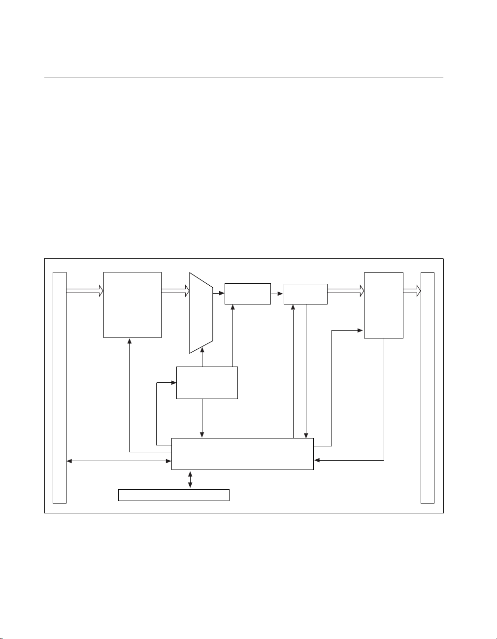
Chapter 1 Introduction
1.1 DAQ-STC Applications
The primary function of the DA Q-STC is to provide timing and control for the A/D and D/A
subsystems of a DAQ board. To understand the DAQ-STC, you should be familiar with a
typical implementation of an A/D and D/A board. This section presents a typical
implementation of these two primary functions and familiarizes you with the components
controlled by the DAQ-STC. The remaining functions, such as digital I/O and
general-purpose counting, are self-contained and independent and can, therefore, be
understood without discussing any specific implementation.
1.1.1 Analog Input Application
Figure 1-1 shows the primary components of an analog input subsystem. On an analog input
board, a sample/hold circuit samples the analog value of one or more input channels, and an
A/D converter (ADC) converts the analog value to a digital value. A FIFO then holds the
digital data until it can be transferred to the host system memory.
Analog
Channels
Sample/Hold
Hold
Clock,
Retransmit
Mux
Select
Configuration
FIFO
Analog
Processing
Gain,
Polarity,
SE/diff
Convert
ADC
Clock
AI Data
FIFO
I/O Connector
FIFO Empty,
Ghost
Timing/Trigger
Analog Input Timing/Control
RTSI Connector
DAQ-STC
Timing/Trigger
Figure 1-1.
Analog Input Application
The analog channels enter the board through the I/O connector, as shown at the left of the
figure. The DA Q-STC supplies a hold command to latch the analog values at the sample/hold
device. On boards with multiple-input channels, a multiplexer selects each channel, one at a
DAQ-STC Technical Reference Manual 1-2
Status
FIFO Status
©
National Instruments Corporation
System Bus
Page 28
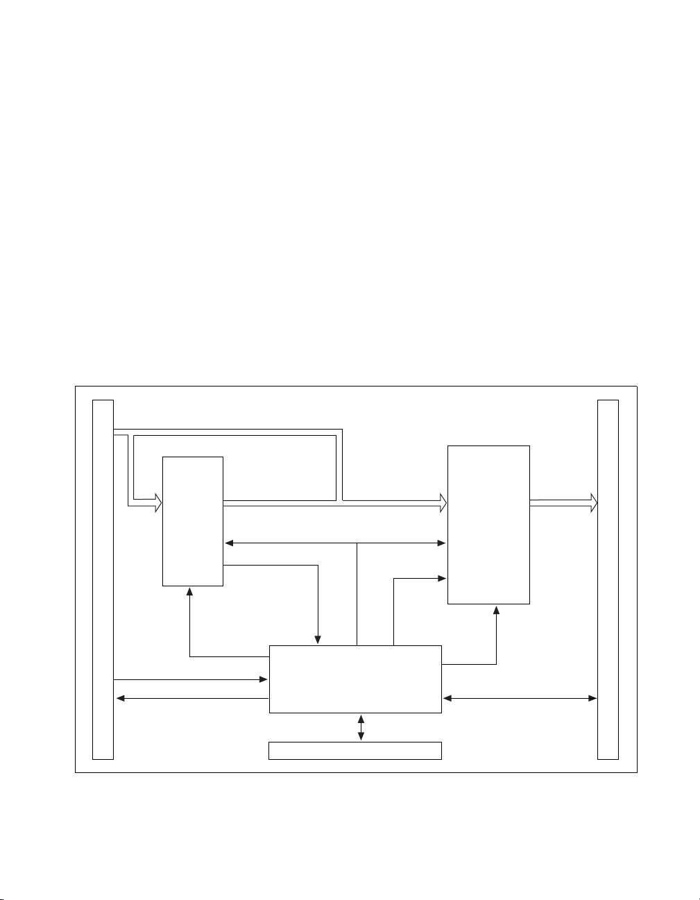
time, and applies its voltage to the ADC. The DAQ-STC instructs the ADC to begin the
conversion and monitors the progress through status flags. When the con v ersion is complete,
the DAQ-STC clocks the digital data into the AI data FIFO until it can be retrieved by the
system bus.
The DA Q-STC monitors the status of the AI data FIFO so that the DA Q-STC can generate an
interrupt or a DMA request when the FIFO fills beyond a programmable threshold. On many
boards, a configuration FIFO is available to provide gain control and channel selection. The
DAQ-STC supplies a clock and a retransmit signal for the configuration FIFO and monitors
the FIFO empty flag. The ghost signal from the configuration FIFO inhibits the AI data FIFO
clock to provide a multirate sampling capability. T iming and trigger signals pass to and from
the DAQ-STC and the I/O and RTSI connectors for external timing applications.
1.1.2 Analog Output Application
Figure 1-2 shows the primary components of an analog output subsystem. On an analog
output board, the CPU typically writes the output data into the AO data FIFO, and one or more
D/A converters (DACs) subsequently convert the digital data to an analog form.
Output Data
Chapter 1 Introduction
Analog
Channels
AO
Data
FIFO
Status
Retransmit
System Bus
CPU Request
Channel Ready
©
National Instruments Corporation 1-3 DAQ-STC Technical Reference Manual
Analog Output Timing/Control
DAC Write
DAQ-STC
RTSI Connector
Figure 1-2.
DAC Address
Timing/Trigger
Analog Output Application
DACs
Update
Timing/Trigger
I/O Connector
Page 29
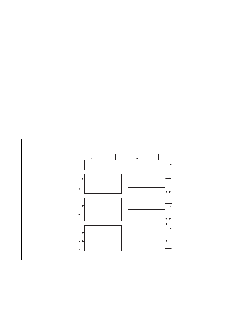
Chapter 1 Introduction
The DA Q-STC monitors the status of the A O data FIFO so that it can generate an interrupt or
a DMA request when the FIFO empties beyond a programmable threshold. The DAQ-STC
can also supply a retransmit signal to the AO data FIFO if the FIFO is large enough to hold
the entire buffer. When the output data is needed at the converters, the DAQ-STC clocks the
data from the FIFO into the DA Cs using the D AC write and DAC address signals. An update
signal allows all of the DACs to update their outputs simultaneously.
The CPU can also write directly to the DA Cs, using the CPU request signal to request that the
DAQ-STC allow access. The DAQ-STC arbitrates between itself and the CPU, notifying the
CPU that the write has completed using the channel ready signal. Timing and trigger signals
pass to and from the DAQ-STC and the I/O and RTSI connectors for external timing
applications.
1.2 DAQ-STC Block Diagram
Figure 1-3 shows a block diagram of the DA Q-STC. The diagram shows all of the I/O signals
as well as the direction of the signal—input, output, or bidirectional. Each chapter of this
manual discusses one of the modules depicted in this block diagram.
A<1..7>
CS, RD/WR, WR/DS
RESET, INTEL/MOTO
D<0..15>
CHRDY_OUTCHRDY_IN
Bus Interface
SOC, EOC, GHOST, AI_STOP_IN
CONVERT, AI_STOP_OUT, AIFREQ
LOCALMUX_CLK, LOCALMUX_FFRT
EXTMUX_CLK, SCAN_IN_PROG
DACWR<0..1>, LDAC<0..1>, AOFREQ
AIFEF, AIFHF, AIFFF
MUXFEF
SHIFTIN, AI_FIFO_SHIFTIN
SC_TC, SI_TC, DIV_TC
AOFEF, AOFHF, AOFFF
CPUDACREQ
TMRDACREQ, TMRDACWR
CPUDACWR, AO_ADDR<0..3>
UPDATE, UPDATE2, AOFFRT
BC_TC, UC_TC
G_UP_DOWN<0..1>
G_OUT0/RTSI_IO
G_OUT1/DIV_TC_OUT
Analog Input
Timing/Control
Analog Output
Timing/Control
General-Purpose
Counter/Timer
Figure 1-3.
DAQ-STC Block Diagram
DAQ-STC Technical Reference Manual 1-4
Programmable
Function Inputs
RTSI Trigger
Interrupt Control
Digital I/O
Miscellaneous
Functions
WRITE_STROBE<0..3>
FFI<0..9>
RTSI_TRIGGER<0..6>
RTSI_BRD<0..3>
RTSI_OSC
IRQ_IN<0..1>
IRQ_OUT<0..7>
SEC_IRQ_OUT_BANK<0..1>
DIO<0..7>
STATUS<0..3>
CONTROL<0..7>
EXTSTROBE/SDCLK
OSC, TEST_IN
ANALOG_TRIG_IN_LO
ANALOG_TRIG_IN_HI
OUTBRD_OSC, FOUT
ANALOG_TRIG_DRIVE
TEST_OUT
©
National Instruments Corporation
Page 30

Analog Input Timing/Control
2.1 Overview
This chapter describes the analog input timing/control module (AITM), which generates
timing for the ADC and controls signals for the associated circuitry. The AITM contains a
24-bit scan interval counter (SI), a 24-bit scan counter (SC), a 16-bit sample interval counter
(SI2), and a 16-bit divide down counter (DIV).
There are eight timing and control signals associated with the analog input. These are the scan
interval clock (SI source), sample interval clock (SI2 source), ADC conversion strobe
(CONVERT), trigger (START1), second trigger (START2), start scan (START), stop scan
(STOP), and external gate. The AITM contains independent multiplexers and conditioning
circuits to derive these timing/control signals from any of 10 programmable function input
(PFI) signals (PFI<0..9>), seven RTSI trigger signals (RTSI_TRIGGER<0..6>), or other
internal signals.
This chapter presents a list of the AITM features, followed by a simplified model that
introduces a few AITM-related signals, an overvie w of each of the AITM modes, a list of the
external pins used by the AITM module, programming information for users who need to
program the hardware at a low level, a complete list of the AITM timing diagrams, and a
detailed description of the internal workings of the AITM. The final section is intended for
advanced users. Read section 1.1.1, Analog Input Application, for more information about
devices with which the AITM can work.
2
2.1.1 Programming the AITM
To program the AITM of the DAQ-STC, read the following:
• Section 1.1.1, Analog Input Application
• Sections 2.2, Features, through 2.6, Programming Information
As you read section 2.6, Programming Information, you will need to refer to section 2.7,
Timing Diagrams. You will also need to consult the register-le vel programmer manual for the
hardware containing the DA Q-STC. If you need additional help programming the AITM, read
section 2.8, Detailed Description.
©
National Instruments Corporation 2-1 DAQ-STC Technical Reference Manual
Page 31

Chapter 2 Analog Input Timing/Control
2.2 Features
The AITM has the following features:
• Scan interval timing
– 24-bit scan interval down counter
– Maximum frequency of 20 MHz yi elds 50 ns resolutio n with a maximum interv al of
0.83 s
– Divide-by-two timebase yields 100 ns resolution with a maximum interval of 1.67 s
– Divide-by-200 timebase yields 10 µs resolution with a maximum interval of 167 s
• Sample interval counter
– 16-bit sample interval down counter
– Maximum sample rate of 10 MS/s
– Maximum interval of 3.3 ms between channels with 50 ns resolution
• External timing for the following signals
–START
–START1
–START2
– CONVERT
– SI source, with special considerations for the SI2 source
–STOP
– External gate
• Bidirectional external timing pins
– Input timing and control signals from PFI<0..9> and RTSI_TRIGGER<0..6>
– Output the most important internally generated timing and control signals to the
board
• Programmable polarities for clock sources, trigger inputs, and the most important timing
outputs
• Ability to change the scan rate during an acquisition, in combination with the GPCT
module or directly in software
• Scan count
– 24-bit scan down counter
– Trigger up to 2
24
scans or generate scans continuously
DAQ-STC Technical Reference Manual 2-2
©
National Instruments Corporation
Page 32

Chapter 2 Analog Input Timing/Control
• Trigger modes
– Hardware and software triggering
– Support for versatile analog triggering
• Delayed trigger
– Interval counters have alternate first period capability for retriggerable delay from
trigger
– Minimum delay of one SI source clock
– Maximum delay of 2
24
SI source clocks
• Pretrigger
– Count pretrigger scans and ignore START2 triggers until the pretrigger count has
been satisfied
– Synchronize multiple DAQ-STCs in th e pretrigg er mode
•Gating
– Hardware and software gating
• Seamless interface to the configuration FIFO and the data FIFO
• Error detection
– Overrun and overflow error-detection flags for internal or external timing
– Error detection for excessive interrupt latency during staged analog input
• Bus interface support
– Interrupts based on triggers, error conditions, and FIFO flags
– FIFO-flag-based request signal to simplify DMA request logic
• Seamless interface to external analog input accessories
– Multiplexer
– 16-bit counter can generate internal multiplexer clock by dividing down the external
multiplexer clock
– Provides a clock for the external multiplexer
– Simultaneous sample and hold
– Generates the track-and hold-signal
©
National Instruments Corporation 2-3 DAQ-STC Technical Reference Manual
Page 33

Chapter 2 Analog Input Timing/Control
2.3 Simplified Model
The AITM contains the hardware necessary to generate timing and control signals for the
ADC and the associated circuitry on a National Instruments DAQ board, such as an MIO
board. Figure 2-1 shows the timing and control signals used in a typical analog input
operation.
START1
START
STOP
CONVERT
Figure 2-1.
Typical Analog Input Waveform
The primary analog input timing signal is the CONVERT pulse, which instructs the ADC to
begin a conversion on the selected analog input channel. CONVER T pulses are organized into
groups called scans. In each scan, the CONVERT signal pulses once for each input channel.
The purpose of the scan grouping is to sample multiple input channels nearly simultaneously.
Each scan begins with a START pulse and ends with a STOP pulse. The START1 trigger
begins the acquisition sequence. Figure 2-1 above depicts an acquisition consisting of three
scans, with each scan sampling four input channels.
DAQ-STC Technical Reference Manual 2-4
©
National Instruments Corporation
Page 34

Figure 2-2 shows a simplified model of the AITM module.
Chapter 2 Analog Input Timing/Control
RTSI_TRIGGER<0..6>
PFI<0..9>
AI_STOP_IN
SOC
EOC
GHOST
AIFFF
AIFHF
AIFEF
SELECT
CONTROL
START1
SC_TC
STOP
START
SI2
COUNTER
SI
COUNTER
SI_TC
DIV_TC
DIV
COUNTER
SC
COUNTER
SI2_TC
OUTPUT
CONVERT
LOCALMUX_CLK
LOCALMUX_FFRT
EXTMUX_CLK
AI_FIFO_SHIFTIN
SHIFTIN
AIFREQ
SCAN_IN_PROG
Figure 2-2. AITM Simplified Model
One of the primary features of the AITM is that a wide variety of signals can be selected as
timing and control sources. The simplified model depicts this as a select circuit, which
chooses between the 10 PFI signals PFI<0..9>, the seven RTSI signals
RTSI_TRIGGER<0..6>, and the dedicated STOP input signal AI_STOP_IN. Many of the
signals required for the ADC can come from external sources routed through the selector . The
DAQ-STC can also generate the timing sources internally.
The simplified model in Figure 2-2 shows that the source for the CONVERT pulse may come
from the SI2 counter (internal CONVERT source) or the select circuit (external CONVERT
source). SOC (start of conversion) and EOC (end of conversion) are status signals generated
by the ADC. SOC indicates that a conv ersion has be gun and EOC indicates that a conversion
is complete.
Using CONVERT as a reference, the output circuit generates several ancillary signals used
on the board. The LOCALMUX_CLK (configuration FIFO advance) signal, which pulses
after an integral number of CONVERTs, advances the configuration FIFO to the next input
channel. The LOCALMUX_FFRT (configuration FIFO retransmit) signal, which pulses
when the configuration FIFO empties, refills the configuration FIFO. The EXTMUX_CLK
(external multiplexer clock) signal, which pulses on e very CONVERT, adv ances the channel
multiplexer . The SHIFTIN signals (AI_FIFO_SHIFTIN and SHIFTIN), which pulse after the
ADC has completed a conversion, move the data into the analog input data FIFO. The
AIFREQ (AI data FIFO request) signal generates a DMA request based on the analog input
©
National Instruments Corporation 2-5 DAQ-STC Technical Reference Manual
Page 35

Chapter 2 Analog Input Timing/Control
FIFO flags AIFEF (AI data FIFO empty flag), AIFHF (AI data FIFO half-full flag), and
AIFFF (AI data FIFO full flag). Refer to section 2.5, Pin Locator Interface, for a complete
description of these signals.
The configuration FIFO may also supply the GHOST signal, which is updated on every
CONVERT. When the GHOST input is active, the AI_FIFO_SHIFTIN pulse is suppressed
following the conversion, so that the ADC data is not shifted into the AI data FIFO. This
feature allows the DAQ-STC to support multirate sampling where channels are sampled at
different input rates.
As shown in Figure 2-2, the STA RT pulse may come from the SI counter (internal START
source) or the PFI selector (external START source). Similarly, the STOP pulse may come
from the DIV counter (internal STOP source) or the PFI selector (external STOP source). The
SCAN_IN_PROG output indicates that a scan is in progress by asserting on START and
deasserting on STOP.
The SC counter is available to count the number of scans that have occurred. This is useful
for generating a specific number of scans in an acquisition. The ST AR T1 trigger signal begins
the acquisition sequence and may come from one of several sources—PFI, R TSI, software, or
general-purpose counter 0.
2.4 Analog Input Functions
The AITM is a highly flexible circuit that can accommodate a variety of timing scenarios. The
most useful of these is the interval scanning mode. For this reason, the functional description
will present interval scanning as the primary analog input mode.
For the purpose of discussion, the analog input functions can be divided into three
groups—low-level timing and control, scan-level timing and control, and acquisition-level
timing and control. Low-level timing and control refers to the timing signals related to and
derived from CONVER T. Scan-level timing and control refers to the timing signals necessary
to organize the CONVERT pulses into scans. Acquisition-level timing and control refers to
the timing signals that govern the generation of scan sequences.
2.4.1 Low-Level Timing and Control
This section discusses CONVERT and the signals derived from CONVERT.
The CONVERT signal is the primary timing signal for analog input. Three board-level
subsystems are controlled by CONVERT and the signals derived from CONVERT—the
ADC, the data FIFO, and the configuration FIFO and external multiplexer . CONVERT timing
is affected by your selection of internal or external CONVERT mode.
DAQ-STC Technical Reference Manual 2-6
©
National Instruments Corporation
Page 36

Chapter 2 Analog Input Timing/Control
2.4.1.1 ADC Control
The basic function of the ADC control signals is to time ADC conversions and load the
resulting digital data into a latch. The primary output signals are CONVERT and SHIFTIN,
and the input signals are SOC and EOC. Figure 2-3 shows these signals in a basic data
acquisition sequence.
CONVERT
SOC
EOC
SHIFTIN
Figure 2-3.
ADC Control
The SOC input informs the DAQ-STC when a conversion starts. Similarly, the EOC input
notifies the DAQ-STC when a conversion completes. The assertion of EOC leads to the
assertion of SHIFTIN, which loads the acquired data into its destination. An overrun
condition occurs when the conversion rate is too high for the A/D subsystem to maintain. If a
second CONVERT signal occurs before the current conversion is complete, the DAQ-STC
flags an overrun error and generates an interrupt if programmed to do so.
2.4.1.2 Data FIFO Control
Many DA Q products include data FIFOs to pre vent loss of data at high speeds and to increase
bus bandwidth. The data FIFO control signals support such a FIFO. The SHIFTIN signal
loads the result of each conversion into the data FIFO. Three status flags indicate the amount
of data stored in the FIFO and are monitored by the DAQ-STC. The three status flags are
AIFFF , AIFHF, and AIFEF. When the FIFO flags indicate that the FIFO lev el has exceeded a
programmed threshold, the DAQ-STC notifies the host computer using either an interrupt
request, if the CPU performs data transfers, or the DMA request signal AIFREQ, if the DMA
controller performs data transfers. The host computer then transfers the input data stored in
the data FIFO to main memory.
2.4.1.3 Configuration FIFO and External Multiplexer Control
Typical DAQ products provide a means of setting channel, gain, polarity, and other
configuration information for the A/D subsystem. Recent products offer the ability to change
this information on a per conversion basis. The DAQ-STC fully supports a FIFO-based
configuration memory that can update on every CONVERT pulse. Typically, the
configuration FIFO contains one data word for each input channel included in the scan. At the
©
National Instruments Corporation 2-7 DAQ-STC Technical Reference Manual
Page 37

Chapter 2 Analog Input Timing/Control
end of the scan, the FIFO read pointer is reset, effectively reloading the FIFO with the
configuration list. The LOCALMUX_CLK signal, which asserts at the same time as
CONVERT, advances the configuration FIFO. At the leading edge of the final
LOCALMUX_CLK, the configuration FIFO becomes empty, causing MUXFEF to assert.
When MUXFEF asserts, LOCALMUX_FFRT pulses on the trailing edge of
LOCALMUX_CLK, causing the configuration FIFO to reload the entire configuration list.
Figure 2-4 shows the operation of these signals during two scans, where each scan contains
four channels.
CONVERT
LOCALMUX_CLK
DIV Counter
EXTMUX_CLK
MUXFEF
LOCALMUX_FFRT
1010
Figure 2-4. Configuration FIFO Control
In addition to supporting the configuration FIFO, the DAQ-STC also supports an external
multiplexer. Typically, analog input boards are limited to eight or 16 input channels. An
external multiplexer overcomes this limitation by time division, multiplexing several analog
signals onto each input channel. Each memory location in the configuration FIFO
corresponds to one input channel. With an external multiplexer, the configuration FIFO does
not advance until all the external channels have been sampled for a given input channel. The
EXTMUX_CLK signal is available to advance the external multiplexer.
T o use the DA Q-STC with an external multiplex er, you load the DIV counter with the number
of external channels corresponding to each input channel. The EXTMUX_CLK signal pulses
on every CONVERT, but the LOCALMUX_CLK signal pulses only when the DIV counter
reaches state 0. Figure 2-5 shows the operation of these signals during a scan where four
external channels are multiplexed onto each of two input channels.
DAQ-STC Technical Reference Manual 2-8
©
National Instruments Corporation
Page 38

START
STOP
CONVERT
EXTMUX_CLK
LOCALMUX_CLK
Chapter 2 Analog Input Timing/Control
DIV Counter
0 3210321 0
Figure 2-5. External Multiplexer Control
2.4.1.4 CONVERT Timing
As discussed in section 2.3, Simplified Model, sequences of CONVERT pulses are organized
into scans, which begin on START and terminate on STOP. The DAQ-STC can generate the
timing for the individual CONVERT pulses using the SI2 counter (internal CONVERT), or
the timing for CONVERT can come from an external source (e xternal CONVERT). With an
external CONVERT, the SI2 counter is unused.
Internal CONVERT
In the internal CONVERT mode, the hardware generates the CONVERT pulses on SI2_TC
(SI2 counter TC). The ST AR T trigger causes the SI2 counter to begin counting and the STOP
trigger causes the SI2 counter to stop counting. Refer to section 2.4.2, Scan-Level Timing and
Control, for more information on the START trigger. The STOP trigger, which asserts after
the appropriate number of conversions, usually comes from the configuration FIFO. A second
option for generating the STOP trigger, an internal STOP, is to configure the DIV counter to
count the number of conversions, load the DIV counter with the number of conversions per
scan, then use the DIV counter TC as the STOP signal. However, you cannot use an internal
STOP and an external multiplexer at the same time because they both use the DIV counter.
The SI2 counter has dual load registers that allow two timing parameters at the CONVERT
timing level. The first parameter , A, gi ves the delay from START to the first CONVERT. The
second parameter, B, giv es the delay between CONVER T pulses. The SI2 reload mode setting
allows the SI2 counter to alternate load registers on every STOP, thus providing the dual
timing feature.
©
National Instruments Corporation 2-9 DAQ-STC Technical Reference Manual
Page 39

Chapter 2 Analog Input Timing/Control
Figure 2-6 shows two scans with four internally timed CONVERT pulses each to indicate the
available timing parameters. The SCAN_IN_PROG output asserts on START and deasserts
at the completion of the scan.
START
STOP
SCAN_IN_PROG
CONVERT (SI2_TC)
Timing Parameter
ABBB ABBB
Figure 2-6. Internal CONVERT Timing
External CONVERT
In the external CONVERT mode, the externally generated CONVERT pulses enter the
DAQ-STC through one of the PFI<0..9> or RTSI_TRIGGER<0..6> inputs. In order to
preserve the concept of interval scanning with an external CONVERT, the STST_GATE
(Start/Stop Gate) is available. The START trigger enables the STST_GATE and the STOP
trigger disables the STST_GATE.
External CONVERT pulses that occur when the STST_GATE is enabled pass through the
DAQ-STC. External CONVERT pulses that occur when the STST_GATE is disabled are
blocked.
Timing for the external CONVERT can be arbitrarily complex depending on the behavior of
the signal you select as the external CONVERT source. Typically, though, you will select a
periodic signal, in which case the only timing parameter available is the delay between
CONVERT pulses. The delay from START to the first CONVERT depends on the
relationship between the START trigger and the external CONVERT and can vary.
Figure 2-7 shows two scans with four externally timed CONVERT pulses each and indicates
how the delay from START to the first CONVERT can vary. The SCAN_IN_PROG output
asserts on the recognition of START and deasserts on STOP.
DAQ-STC Technical Reference Manual 2-10
©
National Instruments Corporation
Page 40

External CONVERT
START
STOP
STST_GATE
SCAN_IN_PROG
CONVERT
Figure 2-7. External CONVERT Timing
Although successive CONVERT pulses in Figure 2-7 are equidistant, they could follow any
other timing.
2.4.2 Scan-Level Timing and Control
As discussed in section 2.3, Simplified Model, sequences of CONVERT pulses are organized
into scans. Each scan begins with a START pulse. The START pulse may come from either
the SI counter (internal START mode) or the PFI selector (external START mode).
Chapter 2 Analog Input Timing/Control
2.4.2.1 Internal START Mode
In the internal START mode, the SI_TC (SI counter TC) signal becomes the START pulse.
The ST AR T1 trigger causes the SI counter to generate the ST ART pulses which continue until
the acquisition sequence is complete. Refer to section 2.4.3, Acquisition-Level Timing and
Control, for more information on the START1 trigger.
The SI counter has dual-load registers that allow for two timing parameters at the START
timing level. The first parameter (A) gives the delay from START1 to the first START. The
second parameter (B) gives the delay between START pulses.
©
National Instruments Corporation 2-11 DAQ-STC Technical Reference Manual
Page 41

Chapter 2 Analog Input Timing/Control
Figure 2-8 shows three scans of four CONVERT pulses each to indicate the timing
parameters that are available.
Timing Parameter
START1
START (SI_TC)
STOP
CONVERT
AB B B
Figure 2-8. Internal START
2.4.2.2 External START Mode
In the external START mode, the externally generated START pulses enter the DAQ-STC
through one of the PFI<0..9> or RTSI_TRIGGER<0..6> inputs or from general-purpose
counter 0. When the counters are armed and a START1 pulse is received, the DAQ-STC is
ready to recognize external START pulses. Each external START initiates a scan, causing the
DAQ-STC to generate CONVERT pulses until a STOP is received. If the external START
pulses occur at a rate higher than the DAQ-STC can maintain, the extra external START
pulses are ignored.
The timing for the external START can be arbitrarily complex depending on the behavior of
the signal you select as the external START source. Typically, though, you will select a
periodic signal, in which case the only timing parameter available is the delay between
START pulses. The delay from START1 to the first START depends on the relationship
between the START1 trigger and the external START and can vary.
DAQ-STC Technical Reference Manual 2-12
©
National Instruments Corporation
Page 42

Chapter 2 Analog Input Timing/Control
Figure 2-9 shows three scans of four CONVERT pulses each, where the scans are initiated by
an external START.
External START
START1
START
STOP
CONVERT
Figure 2-9. External START
In the external START mode, the SI special trigger delay feature of the SI counter allows an
extra timing parameter in the scan timing. This feature allows you to enforce a minimum
delay from the START1 trigger to the first START. When the SI special trigger delay is
enabled, the SI counter blocks external START pulses for a fixed time period after the
START1 trigger. Software can program the SI counter to count edges on the internal
IN_TIMEBASE signal for an absolute time delay, or it can program the SI counter to count
edges on the external START signal for a delay in terms of the number of START pulses
blocked.
Figure 2-10 depicts the SI special trigger delay feature where the SI counter counts edges on
the internal IN_TIMEBASE signal. The START1 pulse causes the SI counter to begin
counting. External START pulses are not recognized until the SI_TC. This feature gives the
user greater control over the external START timing.
External START
START1
SI_TC
START
Figure 2-10. SI Special Trigger Delay
©
National Instruments Corporation 2-13 DAQ-STC Technical Reference Manual
Page 43

Chapter 2 Analog Input Timing/Control
2.4.3 Acquisition-Level Timing and Control
The SC counter is available to control the acquisition-level timing. Two trigger signals are
available for acquisition-level timing—the START1 trigger and the START2 trigger. The
DA Q-STC has three acquisition-level timing modes—posttrigger mode, pretrigger mode, and
continuous acquisition mode. This section discusses the operation of the START1 and
START2 triggers in the context of these three timing modes.
2.4.3.1 Posttrigger Acquisition Mode
In the posttrigger acquisition mode, only one parameter is required—the number of scans to
complete. The START1 pulse initiates the scan sequence. The SC counter counts the number
of scans and terminates the acquisition upon completion of the programmed number of scans.
Posttrigger acquisitions can be retriggerable or nonretriggerable. In the retriggerable mode,
additional START1 pulses that occur after SC_TC initiate additional acquisition sequences.
In the nonretriggerable mode, only one acquisition sequence is allowed. Externally generated
START1 and START2 triggers enter the DAQ-STC through one of PFI<0..9> or
RTSI_TRIGGER<0..6>.
Figure 2-11 shows a single-posttrigger acquisition sequence consisting of three scans.
START1
START
STOP
CONVERT
SC Counter
SC_TC
210
Figure 2-11.
Posttrigger Acquisition Mode
2.4.3.2 Pretrigger Acquisition Mode
In the pretrigger acquisition mode, two parameters are required. The first parameter gives the
pretrigger count requirement; that is, the number of scans that must occur before ST AR T2 can
be recognized. The second parameter gives the posttrigger count requirement; that is, the
number of scans that will occur after START2 is recognized.
DAQ-STC Technical Reference Manual 2-14
©
National Instruments Corporation
Page 44

Chapter 2 Analog Input Timing/Control
The START1 pulse initiates the scan sequence. After the pretrigger count requirement has
been satisfied, the DAQ-STC looks for the START2 trigger while continuing to generate
scans. When the ST AR T2 trigger has been receiv ed, the hardware generates a specific number
of additional scans according to the posttrigger count requirement. Pretrigger acquisitions can
be retriggerable or nonretriggerable. In the retriggerable mode, additional START1 pulses
initiate additional acquisition sequences. In the nonretriggerable mode, only one acquisition
sequence is allowed. Alternatively, START1 can come from general-purpose counter 0.
Figure 2-12 shows a single pretrigger acquisition sequence with a pretrigger count
requirement of four scans and a posttrigger scan requirement of three scans. The total number
of scans acquired before START2 occurs is six because the START2 trigger occurs after the
sixth scan but before the start of the second scan. The vertical lines indicate where the SC
counter transitions occur.
START1
START2
START
STOP
SC Counter
SC_TC
Don't Care
3 21022210
Figure 2-12. Pretrigger Acquisition Mode
2.4.3.3 Continuous Acquisition Mode
In the continuous acquisition mode, the START1 trigger initiates the scan sequence. The
hardware continues to generate scans until the software issues an AI_End_On_End_Of_Scan
command, an AI_End_On_SC_TC command, or a software reset command. The
AI_End_On_End_Of_Scan command terminates the scan sequence at the end of the next
scan. The AI_End_On_SC_TC command terminates the scan sequence at the next SC_TC
(SC counter TC). The software reset command terminates the scan sequence immediately.
©
National Instruments Corporation 2-15 DAQ-STC Technical Reference Manual
Page 45

Chapter 2 Analog Input Timing/Control
2.4.3.4 Staged Acquisition
Staged acquisition refers to the software action required to implement more than one
posttrigger acquisition sequence, each having unique timing parameters. This section
discusses how the software might handle staged acquisition.
In a programming sequence that occurs prior to the START1 trigger, software loads the
parameter values for the first two acquisition sequences. Software also configures the
counters to switch load registers after each acquisition sequence has completed, providing for
the switch from one sequence to the next. While the second sequence is in progress, software
loads the parameters for the third sequence into the unused load registers. Switching between
load registers occurs at the end of each sequence, that is, at SC_TC. This arrangement allows
the software a maximum latency of up to the duration of the sequence in progress to finish
writing the set of values for the next sequence into the alternate load register set.
Error detection is provided in case the next parameter set is not written in the allotted time.
The error-detection circuit is armed on each SC_TC. If a software clear does not occur before
the next SC_TC, the error-detection circuit latches an SC_TC error condition.
2.4.3.5 Master/Slave Trigger
Use master/slave triggers whenever you need DAQ devices with multiple DAQ-STC ASICs
to acquire data in a synchronized manner; that is, when multiple ASICs share the same
ST ART1 and START2 triggers. With master/slave triggering, one DAQ-STC is designated to
be the master trigger ASIC, sourcing the START1 and START2 triggers to the other ASICs
through the PFI<0..9> or RTSI_TRIGGER<0..6> interf ace. This arrangement provides better
synchronization than if all DA Q-STC ASICs recei ve the same START1 and STAR T2 triggers
independently, because different ASICs may synchronize differently.
In master/slave triggering, all DAQ-STC AITMs are timed from a common source. The
master ASIC delays recognition of the START1 and START2 triggers by one source period
to allow the slave ASICs adequate time to receiv e the triggers. On the following source edge,
all of the ASICs simultaneously begin the programmed acquisition sequence. Master/slave
triggering can be used with any of the three acquisition modes—pretrigger, posttrigger, or
continuous acquisition mode.
2.4.4 Gating
The DAQ-STC also supports gating, an additional external control layer. Both an external
source coming through the PFI<0..9> or RTSI_TRIGGER<0..6> interface and software can
supply the optional control signal. Gating provides a mechanism to pause the data acquisition
operation. When the START signal is internally generated (by the SI counter), gating is
available in two modes—free-run and halt. When the START signal is externally generated,
only free-run gating is available. In all modes, the conversion signal CONVERT is gated on
a scan basis; that is, entire scans are gated on or off.
DAQ-STC Technical Reference Manual 2-16
©
National Instruments Corporation
Page 46

Chapter 2 Analog Input Timing/Control
2.4.4.1 Free-Run Gating Mode
In the free-run gating mode, the scan timing continues without interruption while the outputs
are gated off. For the internal START case, the SI counter continues to count regardless of the
gating signal. If the external gate is asynchronous to the SI source (internal ST ART mode) or
to the external ST AR T , the delay between active gate le vel and first con version of a scan varies
and can be as long as one scan interval.
Figure 2-13 shows two scans and the location of the third scan had it not been gated off.
START1
External Gate
START
STOP
CONVERT
STARTs blocked
Figure 2-13.
Free-Run Gating Mode
2.4.4.2 Halt-Gating Mode
Halt-gating mode is available only when the START signal is generated internally. In the
halt-gating mode, the delay from the assertion of the external gate to the next CONVERT is
minimized. The SI counter counts down normally until it reaches a count value of one. At this
point, the behavior of the SI counter depends upon the external gate. If the external gate is
deasserted, the SI counter pauses so that no START pulses are generated. When the external
gate asserts, the START occurs immediately (with jitter of up to one SI source clock period).
The external gate works as a pseudotrigger for a scan in this mode.
©
National Instruments Corporation 2-17 DAQ-STC Technical Reference Manual
Page 47

Chapter 2 Analog Input Timing/Control
Figure 2-14 shows three scans where the second scan has been delayed by the action of the
external gate. START is asserted immediately upon the assertion of the external gate.
START1
External Gate
START (SI_TC)
STOP
CONVERT
2.4.5 Single-Wire Mode
In the single-wire mode, one signal is used as both an external START and an external
CONVERT. Interval-scan timing is still permitted, although the number of timing parameters
is quite limited. Figure 2-15 shows an example of three scans of four CONVERT pulses each
in single-wire mode.
Single Wire
START1
START
SI Counter Paused
Figure 2-14. Halt-Gating Mode
STOP
CONVERT
Figure 2-15. Single-Wire Mode
DAQ-STC Technical Reference Manual 2-18
©
National Instruments Corporation
Page 48

2.5 Pin Locator Interface
The I/O signals relevant to analog input are listed in Table 2-1. An asterisk following a pin
name indicates that the default polarity for that pin is active low.
Pin Type Notation:
IU Input, pull up (50 kΩ)
IU5 Input, pull up (5 kΩ)
O4TU Output, 4 mA sink, 2.5 mA source tri-state, pull up (50 kΩ)
O9TU Output, 9 mA sink, 5 mA source, tri-state, pull up (50 kΩ)
Chapter 2 Analog Input Timing/Control
Table 2-1.
Pin Name Type Description
AIFEF* IU Data FIFO Empty Flag—This input generates the FIFO
interrupt and the FIFO request signal (AIFREQ) based on the
status of the FIFO. The input polarity is selectable, and the
input state can be directly observed in one of the status
registers. Source: AI data FIFO. Related bitfields:
AI_FIFO_Flags_Polarity, AI_FIFO_Empty_St.
AIFFF* IU Data FIFO Full Flag—This input is used to generate the FIFO
interrupt and the FIFO request signal (AIFREQ) based on the
status of the FIFO. The input polarity is selectable, and the
input state can be directly observed in one of the status
registers. Source: AI data FIFO. Related bitfields:
AI_FIFO_Flags_Polarity, AI_FIFO_Full_St.
AIFHF* IU Data FIFO Half-full Flag—This input generates the FIFO
interrupt and the FIFO request signal (AIFREQ) based on the
status of the FIFO. The input polarity is selectable, and the
input state can be directly observed in one of the status
registers. Source: AI data FIFO. Related bitfields:
AI_FIFO_Flags_Polarity, AI_FIFO_Half_Full_St.
AI_FIFO_SHIFTIN* O9TU Data FIFO Write Clock—This output shifts the ADC data
from the ADC into the data FIFO at the end of conversion.
The AI_FIFO_SHIFTIN pulse is asserted on EOC and
remains asserted based on the selected pulsewidth. The
AI_FIFO_SHIFTIN pulse is inhibited for the conv ersions that
occur when the GHOST signal is active. Output polarity is
selectable. Destination: AI data FIFO. Options: Active Low,
Active High. Related bitfields: AI_SHIFTIN_Polarity,
AI_SHIFTIN_Pulse_Width.
Pin Interface
©
National Instruments Corporation 2-19 DAQ-STC Technical Reference Manual
Page 49

Chapter 2 Analog Input Timing/Control
Table 2-1. Pin Interface (Continued)
Pin Name Type Description
AIFREQ O4TU Data FIFO Request—This output is a FIFO request signal
that indicates that the data FIFO contains data that requires
service. The AIFREQ signal is generated directly from the
data FIFO status flags (AIFEF, AIFHF, and AIFFF) and the
internal SC_TC signal. Output polarity is selectable.
Destination: DMA Controller or CPU. Options: Active Low ,
Active High. Related bitfields: AI_AIFREQ_Polarity,
AI_FIFO_Mode.
AI_STOP_IN IU5 Dedicated STOP Input—This input provides a optimized
path for the end-of-scan signal (LAST_CH) from the
configuration FIFO. Internally, the AI_STOP_IN signal is
routed directly to the STOP selector. Source: Configuration
FIFO. Related bitfields: AI_STOP_Select.
AI_STOP_OUT O4TU Dedicated STOP Output—This output reflects the state of the
active high internal STOP signal. The hardware generates
AI_STOP_OUT and the internal STOP signal by passing the
output of the STOP selector through polarity selection, edge
detection, and synchronization. Output polarity is selectable.
Related bitfields: AI_STOP_Select, AI_STOP_Polarity,
AI_STOP_Edge, AI_STOP_Sync, AI_STOP_St.
CONVERT* O9TU ADC Conversion Strobe—This output instructs the ADC to
perform a conversion. The hardw are generates CONVERT by
passing the internal sample clock (SCLK) signal through
pulsewidth and polarity selection circuitry . Output polarity is
selectable. Destination: ADC. Options: Active Low, Active
High, Ground, High Z. Related bitfields:
AI_CONVERT_Output_Select, AI_CONVERT_Pulse,
AI_CONVERT_Original_Pulse,
AI_CONVERT_Pulse_Timebase,
AI_CONVERT_Pulse_Width.
DIV_TC O4TU DIV Counter TC Signal—Output polarity is active high.
Related bitfields: Misc_Counter_TCs_Output_Enable.
DAQ-STC Technical Reference Manual 2-20
©
National Instruments Corporation
Page 50

Chapter 2 Analog Input Timing/Control
Table 2-1. Pin Interface (Continued)
Pin Name Type Description
EOC IU End of Conversion—This input indicates that a conv ersion is
complete. Internally, the EOC signal causes the SHIFTIN
pulse to be generated and causes the overrun error-detection
circuitry to end the overrun-detection interval (in overrun
mode 0). The input polarity is selectable, and the input state
can be directly observed in one of the status registers. Source:
ADC. Related bitfields: AI_EOC_Polarity, AI_EOC_St,
AI_Overrun_Mode.
EXTMUX_CLK O9TU External Multiplexer Clock—This output pulses after each
CONVERT to clock an external multiplexer such as the
AMUX-64, causing the multiplexer to switch to the next
entry in the external scan list. T wo output modes are av ailable
for the EXTMUX_CLK output. In the first mode,
EXTMUX_CLK trails the LOCALMUX_CLK pulse by
0.5 - 1.5 AI_OUT_TIMEBASE periods and has a pulsewidth
of 4.5 AI_OUT_TIMEBASE periods. In the second mode,
EXTMUX_CLK and LOCALMUX_CLK are asserted at the
same time (when LOCALMUX_CLK is asserted), and their
pulsewidths are equal. Output polarity is selectable.
Destination: External Multiplexer. Options: Active Low,
Active High, Ground, High Z. Related bitfields:
AI_EXTMUX_CLK_Output_Select,
AI_EXTMUX_CLK_Pulse,
AI_EXTMUX_CLK_Pulse_Width.
GHOST IU Ghost Input—This active high input masks the
AI_FIFO_SHIFTIN pulses associated with specific channels
to allow multirate scanning. The GHOST signal is produced
by the configuration FIFO containing the scan list. Source:
Configuration FIFO.
©
National Instruments Corporation 2-21 DAQ-STC Technical Reference Manual
Page 51

Chapter 2 Analog Input Timing/Control
Table 2-1. Pin Interface (Continued)
Pin Name Type Description
LOCALMUX_CLK* O4TU Configuration FIFO Advance Clock—This output clocks the
local configuration FIFO containing the scan list, thereby
updating the channel, gain, and channel configuration
selections. The LOCALMUX_CLK pulse is asserted on
CONVERT and remains asserted based on the selected
pulsewidth, with the added condition that SOC must arrive
before the signal is deasserted. When an external multiplexer
is present, the LOCALMUX_CLK signal can be configured
to pulse only after every n conv ersions, where n is determined
by the value in the 16 bit DIV counter . This is useful when an
external multiplexer is used to switch more than one active
channel into a channel in the scan list. Output polarity is
selectable. Destination: Configuration FIFO. Options: Activ e
Low, A ctive High, Ground, High Z. Related bitfields:
AI_LOCALMUX_CLK_Output_Select,
AI_LOCALMUX_CLK_Pulse,
AI_LOCALMUX_CLK_Pulse_Width,
LOCALMUX_FFRT* O9TU Configuration FIFO Retransmit—This output indicates that
the configuration FIFO should repeat the scan list. When
MUXFEF is active, the LOCALMUX_FFRT signal is
asserted on the trailing edge of LOCALMUX_CLK and
remains asserted based on the selected pulsewidth. Output
polarity is active low. Destination: Configuration FIFO.
Related bitfields: AI_LOCALMUX_CLK_Pulse_Width.
MUXFEF IU Configuration FIFO Empty Flag—This input indicates that
the configuration FIFO is empty . The MUXFEF signal is used
to generate the configuration FIFO retransmit signal
(LOCALMUX_FFRT). The input polarity is selectable.
Source: Configuration FIFO. Related bitfields:
AI_FIFO_Flags_Polarity.
DAQ-STC Technical Reference Manual 2-22
©
National Instruments Corporation
Page 52

Chapter 2 Analog Input Timing/Control
Table 2-1. Pin Interface (Continued)
Pin Name Type Description
SCAN_IN_PROG O4TU Scan in Progress—This output indicates that a scan is in
progress. It is useful for generating track/hold signals for on
board track and hold systems in a simultaneous sampling
environment. In the internal CONVERT mode,
SCAN_IN_PROG is asserted when START is recognized. In
the external CONVER T mode, SCAN_IN_PR OG is asserted
on the first CONVERT of each scan. The signal remains
asserted until SOC occurs while the internal STOP is active.
Output polarity is selectable. Destination: Sample and hold
circuit. Options: Active Low, Active High, Ground, High Z.
Related bitfields: AI_SCAN_IN_PROG_Output_Select,
AI_SCAN_IN_PROG_Pulse.
SC_TC O9TU SC Counter TC—This signal indicates the end of a data
acquisition operation. Output polarity is active high. Related
bitfields: Misc_Counter_TCs_Output_Enable.
SHIFTIN* O9TU Data Shift Pulse—This output sends ADC data over the serial
link. The serial link transfers data serially across the RT SI bus
but is not currently supported. The signal is similar to
AI_FIFO_SHIFTIN except that its generation is not inhibited
by the GHOST signal. The SHIFTIN pulse is asserted on
EOC and remains asserted based on the selected pulsewidth.
Output polarity is active low. Destination: Serial Data Link.
Related bitfields: AI_SHIFTIN_Pulse_Width.
SI_TC O4TU SI Counter TC Signal—Output polarity is active high.
Related bitfields: Misc_Counter_TCs_Output_Enable.
SOC IU Start of Conversion—This input indicates that a conversion
has begun. Internally , the SOC signal allo ws the trailing edge
of LOCALMUX_CLK to occur, enables the overrun
error-detection circuitry to start the overrun-detection
interval, and terminates the SCAN_IN_PROG signal (when
STOP is asserted). The input polarity is selectable, and the
input state can be directly observed in one of the status
registers. Source: ADC. Related bitfields: AI_SOC_Polarity ,
AI_SOC_St.
©
National Instruments Corporation 2-23 DAQ-STC Technical Reference Manual
Page 53

Chapter 2 Analog Input Timing/Control
2.6 Programming Information
Programming the DAQ-STC involves writing to and reading from the registers on the chip.
The programming instructions are language independent; that is, they instruct you to write a
value to a given bitfield or register or to detect the state of a bitfield or a register without
presenting the actual code.
This section presents the functions required to implement some common analog input
applications, which are described in pseudocode that refers to the various bitfields. Bitfield
descriptions relevant to the AITM modules are also included. The bitfield descrip tio ns are
intended to be used as a reference. See Appendix B, Register Information, for the DA Q-STC
register map and to locate specific bitfield descriptions in this manual.
A bitfield is a bit in a register, a group of functionally related bits in one register, or a pair of
registers that jointly perform a function. If a bitfield consists of several bits within one
register, the locations of the bits must be contiguous. Pairs of 16-bit registers are needed for
loading and saving the 24-bit counter contents. Each pair of registers is treated as a single
bitfield in this document.
2.6.1 Register and Bitfield Programming Considerations
Several write-only registers on the DAQ-STC contain bitfields that control a number of
functionally independent parts of the chip. To follow the instructions for assigning values to
bitfields, you must set or clear bits without changing the current state of the remaining bits in
the register . Howe v er , writing to these registers af fects all register bits. You cannot read these
registers to determine which bits have been set or cleared in the past; therefore, you should
maintain a software copy of the write-only registers. You can then use this software copy to
determine the status of write-only registers. Because some bitfields get cleared automatically ,
you should keep your software copies current. T o change the state of a single bitfield without
disturbing the remaining bits, perform the following steps:
1. Make a secondary copy of the software copy.
2. Clear the bitfield in the secondary copy.
3. Place the new bitfield value in the secondary copy.
4. Write the value of the secondary copy to the register.
5. If the bitfield is not cleared automatically, update the software copy by replacing it with
secondary copy.
Bitfields that get cleared automatically are called strobe bits. To change the state of a bitfield
that spans over two registers, you need to write to both registers.
DAQ-STC Technical Reference Manual 2-24
©
National Instruments Corporation
Page 54

2.6.2 Windowing Registers
All of the write-only and read-only registers on the DAQ-STC can be addressed in two
modes—direct mode and windowed mode. A particular implementation on a board may use
either or both of these modes.
Direct mode allows direct access to all of the D AQ-STC registers. The register addresses are
calculated by adding the register offset to the base address assigned to the DAQ-STC on the
particular board. The Register Maps section of Appendix B, Register Information, lists the
register offsets.
Windowed mode allo ws a smaller address space requirement for the DA Q-STC at the expense
of requiring more accesses to perform the same task. In this mode, all DAQ-STC register
accesses use the Window_Address_Re gister and Window_Data_Register. Refer to the 7.6.1,
Windowed Mode Register Access Example section of Chapter 7, Digital I/O, for more
information on windowing mode and for an example program.
Chapter 2 Analog Input Timing/Control
Caution
!
When using windowed-mode accesses from an interruptable process, your
application may not function properly if an interrupt occurs between the time that
the address is loaded into the Window_Address_Register and the time that an
access is made from the Window_Data_Register . Make sure that the interrupt does
not disturb the Window_Address_Register during this sensitive period; disable
interrupts during windowed-mode accesses or write the interrupt routines so that
they do not disturb the contents of the Window_Address_Register.
2.6.3 Programming for an Analog Input Operation
This section contains detailed programming information for bit-level programming of the
AITM for specialized applications. The programs are presented in a bottom-up fashion. This
section lists functions that can be used to configure the AITM for various operations. The
functions are then assembled into a complete program in section 2.6.3.16, Analog Input
Program.
Most of the programming sequences presented here must be executed exactly as shown.
Bitfield assignments are defined as pseudocode instructions of the form <bitfield name> =
<value>. Pseudocode sequences enclosed in braces that contain only bitfield assignments can
normally be executed in any order, or simultaneously, if possible. If the sequence must be
executed in exact order, the character ∑ marks the boundary between two groups of
assignments that have to be ex ecuted sequentially . For example, in the follo wing pseudocode,
the first bitfield assignment must be performed first, the second and third assignments may
then be executed in any order, but the fourth bitfield assignment must be executed after the
second and third bitfield assignments. Other programming constructs, such as if-then, should
be executed in the order shown.
©
National Instruments Corporation 2-25 DAQ-STC Technical Reference Manual
Page 55

Chapter 2 Analog Input Timing/Control
{
FOUT_Enable = 0;
∑
FOUT_Timebase_Select = 0 (FOUT_IN_TIMEBASE1) or 1 (IN_TIMEBASE2);
FOUT_Divider = 0 (for division factor 16) or 1-15 (for division factor 1-15);
∑
FOUT_Enable = 1;
}
The directives Begin critical section and End critical section mark the beginning and end of
critical sections in the ensuing pseudocode. All statements under these directives must be
synchronized with the ISRs; in other words, while the code fragment under these directives is
executing in the foreground, all interrupt-time-specific code must be prevented from
executing in the background.
Under some single-tasking operating systems such as DOS, the directives Begin critical
section and End critical section directly map to CLI and STI assembly-language instructions,
respectively . Ho wever , other operating systems may require specific primiti ves to achie ve this
functionality.
2.6.3.1 Resetting
Assume the AITM was set up to perform an unknown operation. The object is to stop any
activities in progress.
Function
{
AI_Reset_All
Begin critical section;
AI_Reset = 1;
∑
AI_Configuration_Start = 1;
∑
AI_SC_TC_Interrupt_Enable = 0;
AI_START1_Interrupt_Enable = 0;
AI_START2_Interrupt_Enable = 0;
AI_START_Interrupt_Enable = 0;
AI_STOP_Interrupt_Enable = 0;
AI_Error_Interrupt_Enable = 0;
AI_FIFO_Interrupt_Enable = 0;
∑
AI_SC_TC_Error_Confirm = 1;
AI_SC_TC_Interrupt_Ack = 1;
AI_START1_Interrupt_Ack = 1;
AI_START2_Interrupt_Ack = 1;
AI_START_Interrupt_Ack = 1;
AI_STOP_Interrupt_Ack = 1;
AI_Error_Interrupt_Ack = 1;
∑
DAQ-STC Technical Reference Manual 2-26
©
National Instruments Corporation
Page 56

Chapter 2 Analog Input Timing/Control
At this point, you should clear your software copies of the registers so that they will agree
with the DAQ-STC registers. The affected registers are:
AI_Command_1_Register,
AI_Command_2_Register,
AI_Mode_1_Register,
AI_Mode_2_Register,
AI_Mode_3_Register,
AI_Output_Control_Register,
AI_Personal_Register,
AI_START_STOP_Select_Register,
AI_Trigger_Select_Register;
∑
Reserved_One = 1;
AI_Start_Stop = 1;
∑
AI_Configuration_End = 1;
End critical section;
}
Y ou need to perform the
AI_Board_Personalize function to bring the AITM into a known
state. You can then program the AITM for any desired operation.
2.6.3.2 Board Power-up Initialization
Part of the AITM programming depends only on properties of the hardware surrounding the
DA Q-STC. If you are programming a D AQ-STC that is part of a data acquisition system, refer
to the document for register-level programming for information about the proper selections to
make in this function.
Function
{
AI_Board_Personalize
Begin critical section;
AI_Configuration_Start = 1;
∑
AI_Source_Divide_By_2 = 0 (AI_IN_TIMEBASE1 equals IN_TIMEBASE) or
1 (AI_IN_TIMEBASE1 is IN_TIMEBASE divided by two);
AI_Output_Divide_By_2 = 0 (AI_OUT_TIMEBASE equals IN_TIMEBASE) or
1 (AI_OUT_TIMEBASE is IN_TIMEBASE divided by
two);
AI_CONVERT_Pulse_Timebase = 0 (pulsewidth is selected by
AI_CONVERT_Pulse_Width) or
1 (pulse width is selected by
AI_CONVERT_Original_Pulse);
©
National Instruments Corporation 2-27 DAQ-STC Technical Reference Manual
Page 57

Chapter 2 Analog Input Timing/Control
AI_CONVERT_Pulse_Width = 0 (1.5–2 AI_OUT_TIMEBASE periods) or
AI_CONVERT_Output_Select = 0 (high Z) or 1 (ground) or 2 (enable, active low) or
AI_FIFO_Flags_Polarity = 0 (active low) or 1 (active high);
AI_LOCALMUXCLK_Pulse_Width = 0 (Retransmit = 0.5–1 AI_OUT_TIMEBASE
AI_AIFREQ_Polarity = 0 (active high) or 1 (active low);
AI_SC_TC_Output_Select = 0 (high Z) or 1 (ground) or 2 (enable, active low) or 3
(enable, active high);
AI_SHIFTIN_Polarity = 0 (active low) or 1 (active high);
AI_SHIFTIN_Pulse_Width = 0 (0.5–1.5 AI_OUT_TIMEBASE periods) or
AI_EOC_Polarity = 0 (rising edge) or 1 (falling edge);
AI_SOC_Polarity = 0 (rising edge) or 1 (falling edge);
1 (0.5–1 AI_OUT_TIMEBASE periods);
3 (enable, active high);
periods, Read = 1.5–2 AI_OUT_TIMEBASE periods) or
1 (Retransmit = 0.5 AI output clock periods,
Read = 0.5–1 AI_OUT_TIMEBASE periods);
1 (1.5–2 AI_OUT_TIMEBASE periods);
AI_Overrun_Mode = 0 (from SOC to EOC) or 1 (from SOC to the trailing edge of
SHIFTIN);
AI_SCAN_IN_PROG Output_Select = 0 (high Z) or 1 (ground) or 2 (enable, active low)
AI_LOCALMUX_CLK_Output_Select = 0 (high Z) or 1 (ground) or 2 (enable, active
∑
AI_Configuration_End = 1;
End critical section;
}
2.6.3.3 Initialize Configuration Memory Output
Use this function to generate a LOCALMUX_CLK pulse that accesses the first value in the
configuration FIFO.
Function
{
DAQ-STC Technical Reference Manual 2-28
AI_Initialize_Configuration_Memory_Output
Begin critical section;
AI_Configuration_Start = 1;
If (an external MUX is present) then
{
AI_External_MUX_Present = 0;
or 3 (enable, active high);
low) or 3 (enable, active high);
©
National Instruments Corporation
Page 58

Chapter 2 Analog Input Timing/Control
∑
AI_CONVERT_Pulse = 1;
∑
/*Pause here long enough that the LOCALMUX_CLK pulse generated by the /
/*CONVERT* will have time to clock the configuration FIFO*/
AI_External_MUX_Present = 1;
}
Else
{
AI_CONVERT_Pulse = 1;
}
AI_Configuration_End = 1;
End critical section;
}
2.6.3.4 Board Environment Setup
Part of the AITM programming depends only on properties of hardware surrounding the
device that the DAQ-STC is on. For example, if you have an MIO board, the external
hardware can be an AMUX-64T or an SCXI device. The major distinction between po wer-up
initialization and environment setup is that power-up initialization is always the same for a
device using the DAQ-STC, while the latter environmental setup may be different.
Function
AI_Board_Environmentalize
{
Begin critical section;
AI_Configuration_Start = 1;
∑
If (an external MUX is present) then
{
AI_EXTMUX_CLK_Output_Select = 2 (enable, active low) or 3 (enable, active high);
/*Base selection on board hardware*/
AI_EXTMUX_CLK_Pulse_Width = 0 (4.5 AI_OUT_TIMEBASE periods) or
1 (same as LOCALMUX_CLK);
If (more than one external MUX channel corresponds to each internal channel) then
{
AI_External_MUX_Present = 1;
∑
AI_DIV_Load_A = number of external channels corresponding to each internal
channel - 1;
∑
AI_DIV_Load = 1;
}
Else
{
AI_External_MUX_Present = 0;
©
National Instruments Corporation 2-29 DAQ-STC Technical Reference Manual
Page 59

Chapter 2 Analog Input Timing/Control
}
}
Else
{
AI_External_MUX_Present = 0;
AI_EXTMUX_CLK_Output_Select = 0 (high Z) or 1 (forced to logic low);
∑
AI_Configuration_End = 1;
End critical section;
}
If AI_External_MUX_Present is set to 1, you should use the DIV counter to account for the
external-to-internal multiplexing factor. In this case, you cannot use the DIV counter to
generate the STOP trigger.
2.6.3.5 FIFO Request
Use this function to select the data FIFO condition on which interrupt or DMA requests will
be generated.
/*Base selection on board hardware*/
Function
FIFO_Request_Selection
{
Begin critical section;
AI_Configuration_Start = 1;
∑
AI_FIFO_Mode = 0 (FIFO not empty) or 1 (FIFO half-full) or 2 (FIFO full) or
3 (FIFO half-full until FIFO empty);
∑
AI_Configuration_End = 1;
End critical section;
}
2.6.3.6 Hardware Gate Programming
Use this function to enable or disable hardware and software gating. If you enable hardware
gating, you also select the signal that controls the gate, the gate polarity , and the gating mode.
Function
{
AI_Hardware_Gating
Begin critical section;
∑
AI_Configuration_Start = 1;
If (external gating is desired) then
{
DAQ-STC Technical Reference Manual 2-30
©
National Instruments Corporation
Page 60

Chapter 2 Analog Input Timing/Control
AI_External_Gate_Select = 1 through 10 (PFI<0..9>) or 11 through 17
(RTSI_TRIGGER<0..6>);
AI_External_Gate_Polarity = 0 (active high; high enables operation) or
1 (active low; low enables operation);
AI_External_Gate_Mode = 0 (free-run gating) or 1 (halt-gating mode);
}
Else
{
AI_External_Gate_Select = 0 (disabled);
}
∑
AI_Configuration_End = 1;
End critical section;
}
2.6.3.7 Software Gate Operation
In order to use the software gate, the hardware gate must also be enabled. If you want to use
both the software and hardware gate at the same time, configure the hardware gate and then
start your application. If you only want to use the software gate, configure the hardware gate
as indicated in section 2.6.3.6, Hardware Gate Programming with the following changes to
the settings:
• AI_External_+Gate_Select = 31;
• AI_External_Gate_Polarity = 1;
Note
The hardware gate must be enabled in order for the software gate to operate
properly.
To use the software gate, issue the following commands:
• To pause analog input:
AI_Software_Gate = 1;
• To resume analog input after pause:
AI_Software_Gate = 0;
Notes
Software and external gating share the gating mode; that is,
AI_External_Gate_Mode determines the mode of operation for both hardware
and software gating.
Software and hardware gating can be used simultaneously without any special
setup. The analog input operation proceeds when neither hardware nor software
gate is in the pause state.
©
National Instruments Corporation 2-31 DAQ-STC Technical Reference Manual
Page 61

Chapter 2 Analog Input Timing/Control
2.6.3.8 Trigger Signals
Use this function to enable or disable retriggering and to select the START1 and START2
signals (if applicable).
Function
{
AI_Trigger_Signals
Begin critical section;
AI_Configuration_Start = 1;
∑
If (retriggerable acquisition) then
AI_Trigger_Once = 0;
Else
AI_Trigger_Once = 1;
If (pretriggered acquisition) then
{
/*Trigger Selection*/
AI_START1_Select = 0 (bitfield AI_START1_Pulse) or 1 through 10 (PFI<0..9>)
If (AI_START1_Select is 0) then
{
AI_START1_Polarity = 0;
AI_START1_Edge = 1;
AI_START1_Sync = 1;
}
Else
{
AI_START1_Polarity = 0 (active high or rising edge) or
AI_START1_Edge = 1;
AI_START1_Sync = 1;
}
/*Second Trigger Selection*/
AI_START2_Select = 0 (bitfield AI_START2_Pulse) or 1 through 10 (PFI<0..9>)
If (AI_START2_Select is 0) then
{
AI_START2_Polarity = 0;
AI_START2_Edge = 1;
AI_START2_Sync = 1;
}
Else
{
AI_START2_Polarity = 0 (active high or rising edge) or
AI_START2_Edge = 1;
AI_START2_Sync = 1;
}
}
or 11 through 17 (RTSI_TRIGGER<0..6>) or
18 (the G_OUT signal from general-purpose counter 0);
1 (active low or falling edge);
or 11 through 17 (RTSI_TRIGGER<0..6>);
1 (active low or falling edge);
DAQ-STC Technical Reference Manual 2-32
©
National Instruments Corporation
Page 62

Else
{
/*Trigger Selection*/
AI_START1_Select = 0 (bitfield AI_START1_Pulse) or 1 through 10 (PFI<0..9>)
If (AI_START1_Select is 0) then
{
AI_START1_Polarity = 0;
AI_START1_Edge = 1;
AI_START1_Sync = 1;
}
Else
{
AI_START1_Polarity = 0 (active high or rising edge) or
AI_START1_Edge = 1;
AI_START1_Sync = 1;
}
}
∑
AI_Configuration_End = 1;
End critical section;
}
Chapter 2 Analog Input Timing/Control
or 11 through 17 (RTSI_TRIGGER<0..6>) or
18 (the G_OUT signal from general-purpose counter 0);
1 (active low or falling edge);
2.6.3.9 Number of Scans
Use this function to select the number of scans to be acquired. In a staged acquisition, the
number of scans to be executed in each stage is contained in an array named
the acquisition is staged, this function will load the initial value of
sc_ticks into the SC load
register to initialize the first stage. The additional values in the array are written as needed by
the interrupt routine (see
Function
AI_Number_Of_Scans
AI_Staged_ISR).
{
Begin critical section;
AI_Configuration_Start = 1;
∑
If (continuous acquisition) then
AI_Continuous = 1; /*Infinite number of scans*/
Else
AI_Continuous = 0;
If (pretriggered acquisition) then
{
AI_Pre_Trigger = 1;
©
National Instruments Corporation 2-33 DAQ-STC Technical Reference Manual
sc_ticks. If
Page 63

Chapter 2 Analog Input Timing/Control
∑
AI_SC_Load_B = minimal number of pretrigger scans to acquire - 1;
∑
AI_SC_Initial_Load_Source = 1;
AI_SC_Reload_Mode = 1 (alternate load register on TC);
}
Else
{
AI_Pre_Trigger = 0;
AI_SC_Initial_Load_Source = 0;
AI_SC_Reload_Mode = 0 (same load register);
}
AI_SC_Load_A = number of posttrigger scans to acquire - 1;
∑
AI_SC_Load = 1;
If (staged acquisition) then
{
AI_SC_Load_B =
∑
AI_SC_Reload_Mode = 0;
∑
AI_SC_Switch_Load_On_TC = 1;
}
∑
AI_Configuration_End = 1;
End critical section;
}
sc_ticks[0] - 1;
2.6.3.10 Start of Scan
Use this function to select the scan start event. You can specify the scan rate by choosing an
internally generated periodic signal to be the START signal. In a staged acquisition, the
number of clocks between START in each stage is contained in an array named
If the acquisition is staged, this function loads the initial value of
register to initialize the first stage. The additional values in the array are written as needed by
the interrupt routine (see
Variable
si_last_load_register introduced in this function will be used later in the
functions for changing the scan rate during an acquisition (
staged acquisition (
Function
AI_Scan_Start
{
Begin critical section;
Declare variable
AI_Configuration_Start = 1;
∑
DAQ-STC Technical Reference Manual 2-34
AI_Staged_ISR).
AI_Staged_ISR).
si_last_load_register;
si_ticks.
si_ticks into the SI load
AI_Scan_Rate_Change) and
©
National Instruments Corporation
Page 64

Chapter 2 Analog Input Timing/Control
If (internal START mode is selected) then
{
AI_SI_Special_Trigger_Delay = 0;
AI_START_Select = 0 (the internal signal SI_TC);
AI_START_Edge = 1;
AI_START_Sync = 1;
AI_START_Polarity = 0;
If (SI counter will use an internal timebase) then
{
AI_SI_Source_Select = 0 (AI_IN_TIMEBASE1) or 19 (IN_TIMEBASE2);
AI_SI_Source_Polarity = 0;
}
Else
{
AI_SI_Source_Select = 1 through 10 (PFI<0..9>) or 11 through 17
(RTSI_TRIGGER<0..6>);
AI_SI_Source_Polarity = 0 (rising edge) or 1 (falling edge);
}
If (acquisition is retriggerable) then
{
/*You can specify a special delay from the START1 trigger to the first start of
scan by preloading SI*/
AI_SI_Load_A = (number of clocks from START1 to first START) - 1;
AI_SI_Initial_Load_Source = 0;
∑
AI_SI_Load = 1;
∑
AI_SI_Load_A = number of clocks between each START - 1;
AI_SI_Reload_Mode = 0;
}
Else if (you will not change the scan rate during the acquisition) then
{
/*You can specify a special delay from the START1 trigger to the first start of */
/*a scan by using reload mode*/
AI_SI_Load_B = number of clocks from START1 to first START - 1;
AI_SI_Load_A = number of clocks between each START - 1;
AI_SI_Initial_Load_Source = 1;
∑
AI_SI_Load = 1;
∑
AI_SI_Initial_Load_Source = 0;
AI_SI_Reload_Mode = 6 (alternate first period on every SC_TC);
}
Else
{
/*Interval from the START1 trigger to the first start of scan is equal to the scan
interval*/
AI_SI_Load_A = number of clocks between each START - 1;
©
National Instruments Corporation 2-35 DAQ-STC Technical Reference Manual
Page 65

Chapter 2 Analog Input Timing/Control
AI_SI_Initial_Load_Source = 0;
AI_SI_Reload_Mode = 0;
∑
AI_SI_Load = 1;
}
AI_SI_Write_Switch = 0;
}
Else /*External START mode is selected*/
{
/*In the single wire for START and CONVERT case, you need to set
AI_START_Sync to 0*/
/*The single wire case is defined by START and CONVERT coming from a
single external source*/
/*with the same polarity*/
/*In other cases, it is safe to set AI_START_Sync to 1*/
/*It is always safe to set AI_START_Edge to 1*/
If (START source and CONVERT source are equal) AND (START and
CONVERT have the same polarity) then
{
AI_START_Select = 1 through 10 (PFI<0..9>) or 11 through 17
AI_START_Sync = 0;
AI_START_Edge = 1;
AI_START_Polarity = 0 (active high or rising edge) or
}
Else
{
AI_START_Select = 1 through 10 (PFI<0..9>) or 11 through 17
AI_START_Sync = 1;
AI_START_Edge = 1;
AI_START_Polarity = 0 (active high or rising edge) or
}
If (SI Special Trigger Delay is used) then
{
AI_SI_Special_Trigger_Delay = 1;
AI_SI_Write_Switch = 0;
If (an internal timebase is used) then
{
AI_SI_Source_Select = 0 (AI_IN_TIMEBASE1) or 19
(IN_TIMEBASE2);
AI_SI_Source_Polarity = 0;
(RTSI_TRIGGER<0..6>) or 18 (bitfield
AI_START_Pulse) or 19 (the G_OUT signal from
general-purpose counter 0);
1 (active low or falling edge);
(RTSI_TRIGGER<0..6>) or 18 (bitfield
AI_START_Pulse) or 19 (the G_OUT signal from
general-purpose counter 0);
1 (active low or falling edge);
DAQ-STC Technical Reference Manual 2-36
©
National Instruments Corporation
Page 66

}
Else
{
}
AI_SI_Load_A = (minimum number of clocks from START1 to first
START) - 1;
AI_SI_Initial_Load_Source = 0;
∑
AI_SI_Load = 1;
}
Else
AI_SI_Special_Trigger_Delay = 0;
}
If (staged acquisition) then
{
AI_SI_Load_B =
AI_SI_Reload_Mode = 0;
AI_SI_Switch_Load_On_SC_TC = 1;
si_last_load_register = B;
}
Else
{
si_last_load_register = A;
}
∑
AI_Configuration_End = 1;
End critical section;
}
Chapter 2 Analog Input Timing/Control
AI_SI_Source_Select = 1 through 10 (PFI<0..9>) or 11 through 17
(RTSI_TRIGGER<0..6>);
AI_SI_Source_Polarity = 0 (rising edge) or 1 (falling edge);
si_ticks[0] - 1;
2.6.3.11 End of Scan
Use this function to select the end-of-scan event. On a typical MIO board, the end-of-scan
event comes from the configuration memory. On a typical board without configuration
memory, the end-of-scan event is generated by the DIV counter. Notice that the DAQ-STC
cannot simultaneously generate end-of-scan events and timing for an external signal
multiplexer.
Function
{
©
National Instruments Corporation 2-37 DAQ-STC Technical Reference Manual
AI_Scan_End
Begin critical section;
AI_Configuration_Start = 1;
∑
If (the end of scan is coming from the outside, either PFI or Configuration FIFO) then
{
Page 67

Chapter 2 Analog Input Timing/Control
AI_STOP_Select = 1 through 10 (PFI<0..9>) or 11 through 17
(RTSI_TRIGGER<0..6>) or 19 (signal present on the AI_STOP_IN pin);
AI_STOP_Edge = 0;
AI_STOP_Polarity = 0 (active high or rising edge) or 1 (active low or falling edge);
AI_STOP_Sync = 1;
/*If you have a vary fast board, you may need to use an asynchronous STOP
(AI_STOP_Sync = 0)*/
}
Else
{
If (more than one channel per scan) then
{
/*DIV counter is used as the STOP source*/
AI_STOP_Select = 0 (DIV_TC);
AI_STOP_Sync = 1;
AI_STOP_Edge = 0;
AI_STOP_Polarity = 0;
AI_DIV_Load_A = number of channels per scan - 1;
∑
AI_DIV_Load = 1;
}
Else
{
/*Force START signal to be always high*/
AI_STOP_Select = 31 (logic low);
AI_STOP_Sync = 0;
AI_STOP_Edge = 0;
AI_STOP_Polarity = 1;
}
}
∑
AI_Configuration_End = 1;
End critical section;
}
2.6.3.12 Convert Signal
Use this function to select the CONVERT signal. You can specify the channel rate by
choosing an internally generated periodic event.
Function
{
DAQ-STC Technical Reference Manual 2-38
AI_CONVERT_Signal
Begin critical section;
AI_Configuration_Start = 1;
∑
If (internal CONVERT mode is selected) then
{
©
National Instruments Corporation
Page 68

Chapter 2 Analog Input Timing/Control
AI_SC_Gate_Enable = 0;
AI_Start_Stop_Gate_Enable = 0;
If (SI2 counter will use internal time) then
{
/*If you want both SI and SI2 to use AI_IN_TIMEBASE1, you must program
SI to select*/
/*AI_IN_TIMEBASE1 and program SI2 to select the SI source*/
If (SI2 will use AI_IN_TIMEBASE1) then
{
If (internal START mode) AND (SI will use AI_IN_TIMEBASE1) then
AI_SI2_Source_Select = 0 (same signal selected as SI source);
Else
AI_SI2_Source_Select = 1 (AI_IN_TIMEBASE1);
}
Else
{
/*If you want SI2 to use IN_TIMEBASE2, program the SI2 counter to */
/*use the same timebase as the SI counter, and then program the SI */
/*counter to use IN_TIMEBASE2. This will work well in one of the */
/*following two cases: you are not using SI at all, or you are using */
/*SI and it uses IN_TIMEBASE2*/
AI_SI2_Source_Select = 0 (same signal selected as SI source);
AI_SI_Source_Select = 19 (IN_TIMEBASE2);
AI_SI_Source_Polarity = 0;
}
}
Else
{
/*You want to use SI2 and you want to use one of the external timebases. */
/*Program the SI2 counter to use the same timebase as the SI counter, */
/*and program the SI counter to use the external timebase of your choice. */
/*This will work well in one of the following are not using SI at all, or you*/
/*are using SI and it uses the timebase you have selected here*/
AI_SI2_Source_Select = 0 (same signal selected as SI source);
AI_SI_Source_Select = 1 through 10 (PFI<0..9>) or
11 through 17 (RTSI_TRIGGER<0..6>);
AI_SI_Source_Polarity = 0 (rising edge) or 1 (falling edge);
}
AI_SI2_Load_A = number of clocks from START to the first CONVERT - 1;
AI_SI2_Initial_Load_Source = 0;
AI_SI2_Load_B = number of clocks between two CONVERT signals within
a scan - 1;
AI_SI2_Reload_Mode = 1 (alternate first period on every STOP);
∑
AI_SI2_Load = 1;
∑
AI_SI2_Initial_Load_Source = 1;
©
National Instruments Corporation 2-39 DAQ-STC Technical Reference Manual
Page 69

Chapter 2 Analog Input Timing/Control
}
Else
{
AI_SC_Gate_Enable = 1;
AI_Start_Stop_Gate_Enable = 1;
AI_CONVERT_Source_Select = 1 through 10 (PFI<0..9>) or
AI_CONVERT_Source_Polarity = 0 (falling edge) or 1 (rising edge);
}
∑
AI_Configuration_End = 1;
End critical section;
}
Another feature the DAQ-STC provides in the external CONVERT mode is SC_GATE
(SC Counter Gate). Similar to the STST_GATE, the SC_GATE provides a mechanism for
blocking the external CONVER T pulses. If you set AI_Start_Stop_Gate_Enable to 0 in the
external CONVERT section of the
selected. The SC_GATE enables the external CONVERT pulses whenever the SC counter is
enabled to count and blocks the external CONVERT pulses whenever the SC counter is not
enabled to count.
11 through 17 (RTSI_TRIGGER<0..6>) or
19 (the G_OUT signal from general-purpose counter 0);
AI_Convert_Signal function, the SC_GATE is
2.6.3.13 Enable Interrupts
Use this function to enable the AITM to generate interrupts.
Function
{
}
DAQ-STC Technical Reference Manual 2-40
AI_Interrupt_Enable
AI_FIFO_Interrupt_Enable = 0 (disabled) or 1 (enabled);
AI_START_Interrupt_Enable = 0 (disabled) or 1 (enabled);
/*START interrupt must be enabled in order for the STOP interrupt to operate*/
If (AI_START_Interrupt_Enable is 1) then
{
AI_STOP_Interrupt_Enable = 0 (disabled) or 1 (enabled);
}
Else
{
AI_STOP_Interrupt_Enable = 0 (disabled);
}
AI_SC_TC_Interrupt_Enable = 0 (disabled) or 1 (enabled);
AI_START1_Interrupt_Enable = 0 (disabled) or 1 (enabled);
AI_START2_Interrupt_Enable = 0 (disabled) or 1 (enabled);
AI_Error_Interrupt_Enable = 0 (disabled) or 1 (enabled);
©
National Instruments Corporation
Page 70

Chapter 2 Analog Input Timing/Control
To generate interrupts, you must also program the interrupt control module. Refer to
Chapter 8, Interrupt Control, for more information on programming the interrupt control
module. To use interrupts, refer also to section 2.6.8, Analog Input-Related Interrupts.
2.6.3.14 Arming
Use this function to arm the analog input counters.
Function
AI_Arming
{
Declare variable
arm_si, arm_si2
;
If (single scan) then
{
AI_DIV_Arm = 1;
AI_End_On_End_Of_Scan = 1;
}
If (internal START mode) OR (SI special trigger delay will be used) then
arm_si = 1;
Else
arm_si = 0;
If (internal CONVERT mode) then
arm_si2 = 1;
Else
arm_si2 = 0;
AI_SC_Arm = 1; /*You must set these four bitfields in a single write*/
AI_SI_Arm =
AI_SI2_Arm =
arm_si;
arm_si2;
AI_DIV_Arm = 1;
}
2.6.3.15 Starting the Acquisition
Use this function to initiate an analog input operation if you have selected software pretrigger
(for pretriggered operation) or software posttrigger (for non-pretriggered operation). This
function does not do anything unless you have selected software pretrigger or posttrigger.
Function
AI_Start_The_Acquisition
{
If (acquisition is pretriggered) then
{
If (software pretrigger) then
AI_START1_Pulse = 1;
}
Else
{
©
National Instruments Corporation 2-41 DAQ-STC Technical Reference Manual
Page 71

Chapter 2 Analog Input Timing/Control
If (software posttrigger) then
AI_START1_Pulse = 1;
}
}
2.6.3.16 Analog Input Program
The previous sections listed functions that you can use to configure the AITM. This section
shows how to organize these functions to implement a general analog input operation. You
can use the following sequence of functions to program the AITM for any analog input
operation.
{
/*Refer to Chapter 10, Miscellaneous Functions, to set up your timebase*/
/*Before beginning the programming sequence, you may want to program the */
/*Configuration FIFO and flush the AI data FIFO, if this is appropriate for your DAQ */
/*device*/
Call
AI_Reset_All;
Call
AI_Board_Personalize;
Call
AI_Initialize_Configuration_Memory_Output
AI_Board_Environmentalize;
Call
Call
AI_FIFO_Request_Selection;
Call
AI_Hardware_Gating;
Call
AI_Trigger_Signals;
Call
AI_Number_Of_Scans;
Call
AI_Scan_Start;
Call
AI_Scan_End;
Call
AI_CONVERT_Signal;
/*You may want to clear the AI data FIFO, if applicable. If you are using an external */
/*multiplexer, such as the AMUX-64T, you must program it here*/
/*If you are using an external track-and-hold module that requires the presence of the
/*SCAN_IN_PROG signal on PFI7, you must program it here*/
Call
AI_Interrupt_Enable;
Call
AI_Arming;
Call
AI_Start_The_Acquisition;
}
;
2.6.4 Single Scan
T o acquire exactly one scan of input, a special programming sequence is required, as follows.
{
Use the programming sequence from section 2.6.3.16, Analog Input Program.
In the function
AI_START_Select = 31 (ground);
AI_START_Polarity = 0;
DAQ-STC Technical Reference Manual 2-42
AI_Scan_Start, set
©
National Instruments Corporation
Page 72

After the programming sequence is complete, issue the following commands:
AI_START_Polarity = 1;
∑
AI_START_Polarity = 0;
}
2.6.5 Change Scan Rate during an Acquisition
You can change the scan rate if you do not have special requirements on the timing for the
ST AR T1 to START in retriggerable analog input or if the acquisition is not retriggerable. This
will not work in the case of retriggerable analog input with nondefault START1 to START
timing. Assume that the sequence of START rates is stored in the array
variable
following function to change the scan rate.
si_ticks_pointer indicates the current position in the array. You can use the
Chapter 2 Analog Input Timing/Control
si_ticks, and the
Function
AI_Scan_Rate_Change
{
If (acquisition is not retriggerable) OR (you will change the scan rate during an
acquisition) then
{
If (
si_last_load_register is 0) then
{
/*If the last load was from the last load register written to, it is all right to */
/*change the rate Otherwise, you cannot change the rate*/
If (AI_SI_Next_Load_Source_St is 0) then
{
AI_SI_Load_B =
si_ticks_pointer + = 1;
si_last_load_register = 1;
si_ticks[si_ticks_pointer] - 1;
If (switch SI load registers on TC) then
AI_SI_Switch_Load_On_TC = 1;
Else
AI_SI_Switch_Load_On_SC_TC = 1;
}
Else
Scan rate change cannot be performed;
}
Else
{
If (AI_SI_Next_Load_Source_St is 1) then
{
AI_SI_Load_A =
si_ticks_pointer + = 1;
si_last_load_register = 0;
si_ticks[si_ticks_pointer] - 1;
If (switch SI load registers on TC) then
AI_SI_Switch_Load_On_TC = 1;
©
National Instruments Corporation 2-43 DAQ-STC Technical Reference Manual
Page 73

Chapter 2 Analog Input Timing/Control
Else
AI_SI_Switch_Load_On_SC_TC = 1;
}
Else
Scan rate change cannot be performed;
}
}
}
2.6.6 Staged Acquisition
In a staged acquisition, software implements more than one posttrigger acquisition sequence,
each having unique timing parameters. The number of scans to be executed in each stage is
contained in an array named
the array and should be initialized to 1. The number of scans for the first two posttrigger
acquisition sequences is programmed in the
The number of clocks between START in each stage is contained in an array named
si_ticks. The variable si_ticks_pointer is a pointer into the array and should be
initialized to 1. The number of clocks for the first two posttrigger acquisition sequences is
programmed in the
AI_Scan_Start function.
sc_ticks. The variable sc_ticks_pointer is a pointer into
AI_Number_Of_Scans function.
The variable
recently and is initialized in the
si_last_load_register indicates which load register was accessed most
AI_Scan_Start function.
The SC_TC interrupt notifies the CPU that the current acquisition sequence is complete so
that the ISR can program the parameters for the next acquisition sequence. After the
parameters are loaded, the ISR checks for an SC_TC error. An SC_TC error occurs if the
parameters for the next acquisition sequence are not written before the end of the current
acquisition sequence.
Use the following function as an ISR for staged acquisitions.
Function
AI_Staged_ISR
{
/*If the last load was from the last load register written to, it is all right to change the */
/*rate. Otherwise, you cannot change the rate*/
If (
si_last_load_register is 0) then
{
AI_SI_Load_B =
If (
sc_ticks[sc_ticks_pointer] is 0) then
si_ticks[si_ticks_pointer] - 1;
{
AI_End_On_SC_TC = 1;
AI_SC_TC_Interrupt_Enable = 0;
}
Else
{
DAQ-STC Technical Reference Manual 2-44
©
National Instruments Corporation
Page 74

AI_SC_Load_B = sc_ticks[si_ticks_pointer] - 1;
AI_SI_Switch_Load_On_SC_TC = 1;
AI_SC_Switch_Load_On_TC = 1;
}
si_ticks_pointer + = 1;
si_last_load_register = 1;
}
Else
{
AI_SI_Load_A =
If (
sc_ticks[sc_ticks_pointer] is 0) then
si_ticks[si_ticks_pointer] - 1;
{
AI_End_On_SC_TC = 1;
AI_SC_TC_Interrupt_Enable = 0;
}
Else
{
AI_SC_Load_A =
sc_ticks[si_ticks_pointer] - 1;
AI_SI_Switch_Load_On_SC_TC = 1;
AI_SC_Switch_Load_On_TC = 1;
}
si_ticks_pointer + = 1;
si_last_load_register = 0;
}
AI_SC_TC_Interrupt_Ack = 1;
/*Check for interrupt latency problems*/
If (AI_SC_TC_Error_St is 0) then
{
AI_SC_TC_Error_Confirm = 1;
}
Else
{
Inform user that an SC_TC error has occurred;
}
}
Chapter 2 Analog Input Timing/Control
2.6.7 Master/Slave Operation Considerations
You can use several DAQ-STCs for synchronized analog input operation. T o do this, connect
the trigger signal to the trigger input of the master DAQ-STC. You also connect the output
equivalents of the triggers from the master DAQ-STC to the sla ve DAQ-STCs. You may use
the RTSI connector to do this.
Note
©
National Instruments Corporation 2-45 DAQ-STC Technical Reference Manual
You must perform the programming sequence described in section 10.8.1,
Programming Clock Distribution, before you execute the sequence given here.
Page 75

Chapter 2 Analog Input Timing/Control
Use the following programming sequence:
{
AI_START1_Disable = 1 for the master DAQ-STC;
AI_Delayed_START1 = 1 for the master DAQ-STC;
AI_Delayed_START1 = 0 for all the slave DAQ-STCs;
If (pretriggered AI) then
{
AI_Delayed_START2 = 1 for the master DAQ-STC;
AI_Delayed_START2 = 0 for all the slave DAQ-STCs;
}
Perform the usual set-up sequence for each DAQ-STC;
/*See programming sequence in Analog Input Program*/
AI_START1_Disable = 0 for the master DAQ-STC;
}
2.6.8 Analog Input-Related Interrupts
The DAQ-STC is designed to be used primarily with a system that supports interrupts. This
section contains instructions on programming the DAQ-STC when it is used in an
environment that supports interrupts.
If the DA Q-STC you want to program is part of a system in which interrupts do not exist, you
can use programming sequences intended for ISRs directly in your application, coupled with
the programming technique known as polling. If you use polling, your application must
periodically read relevant status bitfields and use the values obtained to decide whether to
execute a programming sequence equivalent to the ISRs.
When the DA Q-STC is used in a system in which interrupts can be handled, b ut the handling
is prohibitively slow, you can use the polling technique. However, your system will be
devoted entirely to one application.
For more detailed discussion of interrupts and polling, refer to any introductory computer
architecture textbook. Information on interrupts and polling can also be found in National
Instruments Application Note 010: Prog ramming Interrupts for Data Acquisition on
80x86-Based Computers.
Interrupts related to analog input can be generated on the following analog input conditions:
• Error (overrun or overflow)
•START
•STOP
•START1
•START2
DAQ-STC Technical Reference Manual 2-46
©
National Instruments Corporation
Page 76

Chapter 2 Analog Input Timing/Control
• SC _TC
• FIFO condition
Basic actions required to enable, detect, and acknowledge the analog input-related interrupts
follow .
Error
To enable: AI_Error_Interrupt_Enable
To recognize: AI_Overflow_St and AI_Overrun_St
To acknowledge (and clear): AI_Error_Interrupt_Ack
START
To enable: AI_START_Interrupt_Enable
To recognize: AI_START_St
To acknowledge (and clear): AI_START_Interrupt_Ack
STOP
To enable: AI_STOP_Interrupt_Enable and
AI_START_Interrupt_Enable
To recognize: AI_STOP_St
To acknowledge (and clear): AI_STOP_Interrupt_Ack
START1
To enable: AI_START1_Interrupt_Enable
To recognize: AI_START1_St
To acknowledge (and clear): AI_START1_Interrupt_Ack
START2
To enable: AI_START2_Interrupt_Enable
To recognize: AI_START2_St
To acknowledge (and clear): AI_START2_Interrupt_Ack
SC_TC
To enable: AI_SC_TC_Interrupt_Enable
To recognize: AI_SC_TC_St
To acknowledge (and clear): AI_SC_TC_Interrupt_Ack
FIFO Condition
To enable: AI_FIFO_Interrupt_Enable
To select condition use: AI_FIFO_Mode
To recognize: AI_FIFO_Full_St, AI_FIFO_Half_Full_St, and
AI_FIFO_Empty_St
©
National Instruments Corporation 2-47 DAQ-STC Technical Reference Manual
Page 77

Chapter 2 Analog Input Timing/Control
To clear: You must change the FIFO state by dealing with the
FIFO
All interrupts related to analog input are in interrupt group A.
To select the interrupt line to be used,
Interrupt_A_Output_Select = 0 through 7;
Interrupt_A_Enable = 1;
To determine quickly if any of the group A interrupts have occurred, use Interrupt_A_St.
Notes To select interrupt output polari ty, use Interrupt_Output_Polarity. This selection
depends on the board hardware design.
Pass_Through_0_Interrupt is also in interrupt group A.
For more detailed information about the conditions that generate an interrupt, refer to
section 2.8.4, Interrupt Control.
2.6.9 Bitfield Descriptions
Bits in the register bit maps are organized into bitfields. A bitfield can contain one or more
bits. Only bits with contiguous locations within a register can belong to a bitfield. The high
and low pairs of load and save registers for 24-bit counters are also treated as bitfields. The
AITM-related bitfields are described below. Not all bitfields referred to in section 2.6,
Programming Information, are listed here. To locate a particular bitfield description within
this manual, refer to Appendix B, Register Information.
AI_AIFREQ_Polarity
bit: 4 type: Write in: AI_Personal_Register address: 77
This bit selects the polarity of the AIFREQ output signal:
0: Active high.
1: Active low.
AI_Analog_Trigger_Reset
bit: 14 type: Strobe in: AI_Command_1_Register address: 8
This bit clears the hysteresis registers in the analog trigger circuit. Set this bit to 1 at the time
you arm the analog input counters if you want to use analog triggering in hysteresis mode for
any analog input signal. Before setting this bit to 1, make sure that the analog trigger is not
being used by any other part of the DAQ-STC. You should not set this bit to 1 in any other
case. This bit is cleared automatically.
DAQ-STC Technical Reference Manual 2-48
©
National Instruments Corporation
Page 78

Chapter 2 Analog Input Timing/Control
AI_Configuration_End
bit: 8 type: Strobe in: Joint_Reset_Register address: 72
This bit clears AI_Configuration_Start, which holds the analog input circuitry in reset to
prevent glitches on the output pins during configuration. You should set this bit to 1 when
ending the configuration of the analog input circuitry. This bit is cleared automatically.
Related bitfields: AI_Configuration_Start.
AI_Configuration_Start
bit: 4 type: Strobe in: Joint_Reset_Register address: 72
This bit holds the analog input circuitry in reset to prevent glitches on the output pins during
configuration. The following analog input circuits are affected:
• Output circuits
• Counter control circuits
• Trigger circuits
• Interrupt circuits
The following circuits are also affected:
• Interrupt_A_Ack_Register
• Autoacknowledge circuit for general-purpose counter 0.
You should set this bit to 1 when beginning the configuration of the analog input circuitry.
By doing this you ensure that no spurious glitches appear on the output pins and on the
internal circuit components. If you do not set this bit to 1, the DAQ-STC may behave
erroneously. This bit is cleared by setting AI_Configuration_End to 1. Related bitfields:
AI_Configuration_End.
AI_Config_Memory_Empty_St
bit: 6 type: Read in: Joint_Status_2_Register address: 29
This bit indicates the state of the MUXFEF input pin (after the polarity selection). Related
bitfields: AI_FIFO_Flags_Polarity.
AI_Continuous
bit: 1 type: Write in: AI_Mod e_1_ Register address: 12
This bit determines the behavior of the SC, SI, SI2, and DIV counters during SC_TC:
0: If AI_Pre_Trigger is 0, the counters will return to idle on the first SC_TC. If
AI_Pre_Trigger is 1, the counters will return to idle on the second SC_TC.
1: The counters will ignore SC_TC.
Set this bit to 0 to select the pretrigger or posttrigger acquisition modes if you want to acquire
a predetermined number of scans. Set this bit to 1 to select the continuous acquisition mode
if you wish to continuously acquire data or to perform staged analog input. You can use
AI_End_On_End_Of_Scan and AI_End_On_SC_TC to stop an analog input operation in the
continuous acquisition mode. Related bitfields: AI_End_On_End_Of_Scan,
AI_End_On_SC_TC, AI_Pre_Trigger.
©
National Instruments Corporation 2-49 DAQ-STC Technical Reference Manual
Page 79

Chapter 2 Analog Input Timing/Control
AI_CONVERT_Original_Pulse
bit: 9 type: Write in: AI_Personal_Register address: 77
If AI_CONVERT_Pulse_Timebase is 1, this bit determines the pulsewidth of the CONVERT
and PFI2/CONV signals. The pulsewidth of the CONVERT signals is:
0: Equal to the pulsewidth of the signal used to generate the CONVERT signal, with
the maximum pulsewidth determined by AI_CONVERT_Pulse_Width.
1: Equal to the pulsewidth of the signal used to generate the CONVERT signal.
Related bitfields: AI_CONVERT_Pulse_Timebase, AI_CONVERT_Pulse_Width.
AI_CONVERT_Output_Select
bits: <0..1> type: Write in: AI_Output_Control_Reg ister address: 60
This bit enables and selects the polarity of the CONVERT output signal:
0: High Z.
1: Ground.
2: Enable, active low.
3: Enable, active high.
This bitfield also selects the polarity of the PFI2/CONV output signal, if enabled for output:
0: Active low.
1: Ground.
2: Active low.
3: Active high.
Related bitfields: BD_2_Pin_Dir.
AI_CONVERT_Pulse
bit: 0 type: Strobe in: AI_Command_1_Register address: 8
Setting this bit to 1 produces a pulse on the CONVERT and PFI2/CONV output signals, if the
signals are enabled for output and if CONVERT pulses are not blocked. CONVERT pulses
can be blocked by the external gate, the software gate, the start/stop gate, or the SC gate. The
pulsewidths of the output signals are determined by AI_CONVERT_Pulse_Width. This bit is
cleared automatically. This bit is disabled when AI_Configuration_Start is set to 1. Related
bitfields: AI_CONVERT_Output_Select, BD_2_Pin_Dir, AI_CONVERT_Pulse_Width.
AI_CONVERT_Pulse_Timebase
bit: 11 type: Write in: AI_Personal_Register address: 77
This bit determines how the pulsewidths of the CONVERT and PFI2/CONV signals are
selected:
0: Selected by AI_CONVERT_Pulse_Width.
1: Selected by AI_CONVERT_Original_Pulse.
Related bitfields: AI_CONVERT_Pulse_Width, AI_CONVERT_Original_Pulse.
DAQ-STC Technical Reference Manual 2-50
©
National Instruments Corporation
Page 80

Chapter 2 Analog Input Timing/Control
AI_CONVERT_Pulse_Width
bit: 10 type: Write in: AI_Personal_Register address: 77
If AI_CONVERT_Pulse_Timebase is 0, this bit determines the pulsewidth of the CONVERT
and PFI2/CONV output signals. If AI_CONVERT_Pulse_Timebase is 1 and
AI_CONVERT_Original_Pulse is 0, this bit determines the maximal pulsewidth of the
CONVERT and PFI2/CONV signals (so that the pulsewidth is equal to the shorter of this
pulsewidth and the original signal pulsewidth). The pulsewidths are as follows:
0: 1.5–2 AI_OUT_TIMEBASE periods.
1: 0.5–1 AI_OUT_TIMEBASE periods.
Related bitfields: AI_CONVERT_Pulse_Timebase, AI_CONVERT_Original_Pulse.
AI_CONVERT_Source_Polarity
bit: 5 type: Write in: AI_Mod e_1_ Register address: 12
This bit selects the of active edge of the CONVERT source (the signal that is selected by
AI_CONVERT_Source_Select):
0: Falling edge.
1: Rising edge.
You must set this bit to 0 in the internal CONVERT mode. Related bitfields:
AI_CONVERT_Source_Select.
AI_CONVERT_Source_Select
bits: <11..15> type: Write in: AI_Mode_1_Register address: 12
This bitfield selects the CONVERT source:
0: The internal signal SI2_TC, inverted..
1–0: PFI<0..9>.
11–17: RTSI_TRIGGER<0..6>.
19: The internal signal GOUT from general-purpose counter 0.
31: Logic low.
When you set this bit to 0, the DAQ-STC is in the internal CONVERT mode. When you select
any other signal as the CONVERT source, the DAQ-STC is in the external CONVERT mode.
AI_Delayed_START
bit: 9 type: Write in: AI_Mod e_3_ Register address: 87
This bit determines when the START1 trigger is used by the AITM:
0: Use START1 trigger immediately.
1: Delay the START1 trigger by synchronizing it to the CONVERT source.
Set this bit to 1 in the master ASIC during master/slave trigger. The slave ASIC(s) can then
synchronize to the same clock as the master by triggering on the START1 signal that is output
from the master.
©
National Instruments Corporation 2-51 DAQ-STC Technical Reference Manual
Page 81

Chapter 2 Analog Input Timing/Control
AI_Delayed_START2
bit: 10 type: Write in: AI_Mode_3_Register address: 87
This bit determines when the START2 trigger is used by the AITM:
0: Use START2 trigger immediately.
1: Delay the START2 trigger by synchronizing it to the CONVERT source.
Set this bit to 1 in the master ASIC during master/slave trigger. The slave ASIC can then
synchronize to the same clock as the master by triggering on the START2 signal that is output
from the master.
AI_Delay_START
bit: 14 type: Write in: AI_Mode_3_Register address: 87
This bit selects the internal clock that synchronizes the START trigger when START
synchronization is selected:
0: START synchronizes to SI2_SRC (internal CONVERT) or to FSCLK (external
CONVERT).
1: START synchronizes to SC_SRC.
Since the clock SC_SRC is internally delayed relative to SI2_SRC and FSCLK, setting this
bit to 1 provides additional margin for the external START to reach the synchronization
flip-flop, but allows less margin for the output of the synchronization flip-flop to reach the
counter control circuits. You should normally set this bit to 0.
Related bitfields: AI_START_Sync.
AI_Disarm
bit: 13 type: Strobe in: AI_Command_1_Register address: 8
Setting this bit to 1 asynchronously disarms the SC, SI, SI2, and DIV counters. This command
should only be used to disarm idle counters. To disarm non-idle counters, use
AI_Software_Reset. This bit is cleared automatically.
Related bitfields: AI_Software_Reset.
AI_DIV_Arm
bit: 8 type: Strobe in: AI_Command_1_Register address: 8
This bit arms the DIV counter. The counter remains armed (and the bit remains set) until it is
disarmed, either by hardware or by setting AI_Disarm to 1. Related bitfields:
AI_DIV_Armed_St, AI_Disarm.
DAQ-STC Technical Reference Manual 2-52
©
National Instruments Corporation
Page 82

Chapter 2 Analog Input Timing/Control
AI_DIV_Armed_St
bit: 14 type: Read in: AI_Status_2_Register address: 5
This bit indicates whether the DIV counter is armed:
0: Disarmed.
1: Armed.
Related bitfields: AI_DIV_Arm.
AI_DIV_Load
bit: 7 type: Strobe in: AI_Command_1_Register address: 8
If the DIV counter is disarmed, this bit loads the DIV counter with the contents of the DIV
load register. If the DIV counter is armed, writing to this bit has no effect. This bit is cleared
automatically.
AI_DIV_Load_A
bits: <0..15> type: Write in: AI_DIV_Load_A_Register address: 64
This bitfield is the load register for the DIV counter. The DIV counter loads the value
contained in this bitfield on AI_DIV_Load and on DIV_TC. Related Bitfields:
AI_DIV_Load.
AI_DIV_Q_St
bit: 13 type: Read in: AI_Status_2_Register address: 5
This bit reflects the state of the DIV control circuit:
0: WAIT.
1: CNT.
See section 2.8, Detailed Description, for more information on the DIV control circuit.
AI_DIV_Save_Value
bits: <0..15> type: Read in: AI_DIV_Save_Register address: 26
This bitfield reflects the contents of the DIV counter. Reading from this bitfield while the DIV
counter is counting may result in an erroneous value.
AI_End_On_End_Of_Scan
bit: 14 type: Strobe in: AI_Command_2_Register address: 4
Setting this bit to 1 disarms the SC, SI, SI2, and DIV counters at the next STOP. You can use
this bit to stop the acquisition in continuous acquisition mode. This bit is cleared
automatically. Related bitfields: AI_Continuous.
©
National Instruments Corporation 2-53 DAQ-STC Technical Reference Manual
Page 83

Chapter 2 Analog Input Timing/Control
AI_End_On_SC_TC
bit: 15 type: Strobe in: AI_Command_2_Register address: 4
Setting this bit to 1 disarms the SC, SI, SI2, and DIV counters at the next SC_TC. You can
use this bit to stop the acquisition in continuous acquisition mode. This bit is cleared
automatically. Related bitfields: AI_Continuous.
AI_EOC_Polarity
bit: 14 type: Write in: AI_Personal_Register address: 77
This bit determines which edge of the EOC input signal indicates end of conversion:
0: Rising edge.
1: Falling edge.
Related bitfields: AI_EOC_St.
AI_EOC_St
bit: 4 type: Read in: Joint_Status_2_R egister address: 29
This bit indicates the state of the EOC pin (after the polarity selection). This bit is useful for
device diagnostic applications. Related bitfields: AI_EOC_Polarity.
AI_Error_Interrupt_Ack
bit: 13 type: Strobe in: Interrupt_A_Ack_ Register address: 2
Setting this bit to 1 clears AI_Overflow_St and AI_Overrun_St and acknowledges the Error
interrupt request (in either interrupt bank) if the Error interrupt is enabled. This bit is cleared
automatically. Related bitfields: AI_Overflow_St, AI_Overrun_St,
AI_Error_Interrupt_Enable.
AI_Error_Interrupt_Enable
bit: 5 type: Write in: In terrupt_A_Enable_Register address: 73
This bit enables the Error interrupt:
0: Disabled.
1: Enabled.
The Error interrupt is generated on the detection of an overrun or overflow error condition.
AI_Error_Second_Irq_Enable
bit: 5 type: Write in: Second_ Irq_A_ E nable_Register address: 74
This bit enables the Error interrupt in the secondary interrupt bank:
0: Disabled.
1: Enabled.
The Error interrupt is generated on the detection of an overrun or overflow error condition.
DAQ-STC Technical Reference Manual 2-54
©
National Instruments Corporation
Page 84

Chapter 2 Analog Input Timing/Control
AI_External_Gate_Mode
bit: 8 type: Write in: AI_Mod e_3_ Register address: 87
This bit determines the gating mode, if gating is enabled.
0: Free-run gating mode.
1: Halt-gating mode.
Refer to section 2.4.4, Gating, for more information on gating modes. Related bitfields:
AI_External_Gate_Select, AI_Software_Gate.
AI_External_Gate_Polarity
bit: 5 type: Write in: AI_Mod e_3_ Register address: 87
This bit selects the polarity of the external gate signal:
0: Active high (high enables operation).
1: Active low (low enables operation).
AI_External_Gate_Select
bits: <0..4> type: Write in: AI_Mode_3_Register address: 87
This bitfield enables and selects the external gate:
0: External gate disabled.
1–10: PFI<0..9>.
11–17: RTSI_TRIGGER<0..6>.
31: Logic low.
You can use the external gate to pause an analog input operation in progress. Refer to
section 2.4.4, Gating, for more information on external gating. Related bitfields:
AI_External_Gate_Polarity.
AI_External_Gate_St
bit: 10 type: Read in: Joint_Status_1_Register address: 27
This bit indicates whether the external gate and the software gate are set to enable analog
input operation:
0: Pause analog input operation.
1: Enable analog input operation.
Related bitfields: AI_External_Gate_Select, AI_Software_Gate.
©
National Instruments Corporation 2-55 DAQ-STC Technical Reference Manual
Page 85

Chapter 2 Analog Input Timing/Control
AI_External_MUX_Present
bit: 12 type: Write in: AI_Mode_2_Register address: 13
This bit determines when the LOCALMUX_CLK output signal pulses:
0: Pulse on every CONVERT.
1: Pulse only on CONVERTs that occur during DIV_TC.
This bit allows you to use the DIV counter for LOCALMUX_CLK signal control. This is
useful if one or more external multiplexers, such as an AMUX-64T or SCXI, are connected
to the board the DAQ-STC is on. You should set this bit to 0 if no external multiplexers are
present or if each external channel corresponds to one internal channel. You should set this
bit to 1 if one or more external multiplexers are present and if you are multiplexing more than
one external channel onto each internal channel. If this bit is set to 1, the DIV counter must
be used to determine the number of EXTMUX_CLK pulses that will correspond to one
LOCALMUX_CLK pulse.
AI_EXTMUX_CLK_Output_Select
bits: <6..7> type: Write in: AI_Output_Control_Reg ister address: 60
This bit enables and selects polarity for the EXTMUX_CLK output signal:
0: High Z.
1: Ground.
2: Enable, active low.
3: Enable, active high.
AI_EXTMUX_CLK_Pulse
bit: 3 type: Strobe in: AI_Command_1_Register address: 8
Setting this bit to 1 produces a pulse on the EXTMUX_CLK output signal if the output is
enabled. The pulsewidth is determined by AI_EXTMUX_CLK_Pulse_Width. This bit is
cleared automatically. Related bitfields: AI_EXTMUX_CLK_Output_Select,
AI_EXTMUX_CLK_Pulse_Width.
AI_EXTMUX_CLK_Pulse_Width
bit: 6 type: Write in: AI_Personal_Register address: 77
This bit selects the pulsewidth and assertion time of the EXTMUX_CLK output signal:
0: Pulsewidth is 4.5 AI_OUT_TIMEBASE periods. EXTMUX_CLK trails the
LOCALMUX_CLK pulse by 0.5–1.5 AI_OUT_TIMEBASE periods.
1: Pulsewidth is equal to the pulsewidth of the LOCALMUX_CLK read pulse selected
by AI_LOCALMUX_CLK_Pulse_Width. EXTMUX_CLK and
LOCALMUX_CLK are asserted at the same time.
Related bitfields: AI_LOCALMUX_CLK_Pulse_Width.
DAQ-STC Technical Reference Manual 2-56
©
National Instruments Corporation
Page 86

Chapter 2 Analog Input Timing/Control
AI_FIFO_Empty_St
bit: 12 type: Read in: AI_Status_1_Register address: 2
This bit reflects the state of the AIFEF pin (after the polarity selection), which indicates the
AI data FIFO status:
0: Not empty.
1: Empty.
Related bitfields: AI_FIFO_Flags_Polarity.
AI_FIFO_Flags_Polarity
bit: 8 type: Write in: AI_Personal_Register address: 77
This bit selects the polarity of the AI data FIFO flags (input signals AIFFF, AIFHF, AIFEF,
and MUXFEF):
0: Active low.
1: Active high.
Related bitfields: AI_FIFO_Empty_St, AI_FIFO_Full_St, AI_FIFO_Half_Full_St,
AI_Config_Memory_Empty_St.
AI_FIFO_Full_St
bit: 14 type: Read in: AI_Status_1_Register address: 2
This bit reflects the state of the AIFFF pin (after the polarity selection), which indicates the
AI data FIFO status:
0: Not full.
1: Full.
Related bitfields: AI_FIFO_Flags_Polarity.
AI_FIFO_Half_Full_St
bit: 13 type: Read in: AI_Status_1_Register address: 2
This bit reflects the state of the AIFHF pin (after the polarity selection), which indicates the
AI data FIFO status:
0: Half-full or less.
1: More than half-full.
Related bitfields: AI_FIFO_Flags_Polarity.
©
National Instruments Corporation 2-57 DAQ-STC Technical Reference Manual
Page 87

Chapter 2 Analog Input Timing/Control
AI_FIFO_Interrupt_Enable
bit: 7 type: Write in: In terrupt_A_Enable_Register address: 73
This bit enables the FIFO interrupt:
0: Disabled.
1: Enabled.
The FIFO interrupt is generated on the FIFO condition indicated by AI_FIFO_Mode. Related
bitfields: AI_FIFO_Mode.
AI_FIFO_Mode
bits: <6..7> type: Write in: AI_Mode_3_Register address: 87
This bit selects the AI data FIFO condition on which to generate the DMA request (output
signal AIFREQ) and the FIFO interrupt (if the FIFO interrupt is enabled):
0: Generate DMA request and FIFO interrupt on FIFO not empty. Keep the request and
interrupt asserted while the FIFO is not empty.
1: Generate DMA request and FIFO interrupt on FIFO more than half-full. Keep the
request and interrupt asserted while the FIFO is half-full.
2: Generate DMA request and FIFO interrupt on FIFO full. Keep the request and
interrupt asserted while the FIFO is full.
3: Generate DMA request and FIFO interrupt on FIFO more than half-full. Keep the
request and interrupt asserted while the FIFO is not empty.
Selection 3 will cause the request and FIFO interrupt to assert at the end of the acquisition and
remain asserted until the FIFO empties, provided that SHIFTIN arrives after the trailing edge
of the last SC_TC. The SHIFTIN signal may arrive before the trailing edge of the last SC_TC
if an internal CONVERT is used and the SI2 clock is slow with respect to the ADC interval.
In this case, you should use the SC_TC interrupt to initiate the final FIFO read at the end at
the acquisition. Related bitfields: AI_FIFO_Interrupt_Enable,
AI_FIFO_Second_Irq_Enable.
AI_FIFO_Request_St
bit: 1 type: Read in: AI_Status_1_Register address: 2
This bit indicates the status of the DMA request (output pin AIFREQ) and the FIFO interrupt:
0: Not asserted.
1: Asserted.
AI_FIFO_Mode selects the condition on which to generate the DMA request and FIFO
interrupt. Related bitfields: AI_FIFO_Mode.
DAQ-STC Technical Reference Manual 2-58
©
National Instruments Corporation
Page 88

Chapter 2 Analog Input Timing/Control
AI_FIFO_Second_Irq_Enable
bit: 7 type: Write in: Second_ Irq_A_ E nable_Register address: 74
This bit enables the FIFO interrupt in the secondary interrupt bank:
0: Disabled.
1: Enabled.
The FIFO interrupt is generated on the FIFO condition indicated by AI_FIFO_Mode. Related
bitfields: AI_FIFO_Mode.
AI_Last_Shiftin_St
bit: 15 type: Read in: Joint_Status_1_Register address: 27
This bit indicates that the last SHIFTIN of the acquisition has occurred. The bit is set on the
SHIFTIN following the SC_TC trailing edge. It is cleared by setting
AI_SC_TC_Interrupt_Ack to 1. Related bitfields: AI_SC_TC_Interrupt_Ack.
Note
If the SC_CLK is slow with respect to the conversion period, the trailing edge of
SC_TC may miss the SHIFTIN pulse. This can happen in the internal CONVERT
mode if you select IN_TIMEBASE2 as the SI2 source. For this reason, you must
not rely on this bit as an end of acquisition indicator.
AI_LOCALMUX_CLK_Output_Select
bits: <4..5> type: Write in: AI_Output_Control_Reg ister address: 60
The bitfield enables and selects the polarity of the LOCALMUX_CLK output signal:
0: High Z.
1: Ground.
2: Enable, active low.
3: Enable, active high.
AI_LOCALMUX_CLK_Pulse
bit: 2 type: Strobe in: AI_Command_1_Register address: 8
Setting this bit to 1 produces a pulse on the LOCALMUX_CLK output signal, if the output
is enabled. The pulsewidth of the output signal is determined by
AI_LOCALMUX_CLK_Pulse_Width. LOCALMUX_CLK must also be cleared by an SOC.
This bit is cleared automatically. Related bitfields: AI_LOCALMUX_CLK_Output_Select,
AI_LOCALMUX_CLK_Pulse_Width
AI_LOCALMUX_CLK_Pulse_Width
bit: 5 type: Write in: AI_Personal_Register address: 77
This bit selects the pulsewidth of the LOCALMUX_FFRT output signal and the minimum
pulsewidth of the LOCALMUX_CLK output signal:
0: LOCALMUX_FFRT is 0.5–1 AI_OUT_TIMEBASE periods and
©
National Instruments Corporation 2-59 DAQ-STC Technical Reference Manual
Page 89

Chapter 2 Analog Input Timing/Control
LOCALMUX_CLK is 1.5–2 AI_OUT_TIMEBASE periods.
1: LOCALMUX_FFRT is 0.5 AI_OUT_TIMEBASE periods and LOCALMUX_CLK
is 0.5–1 AI_OUT_TIMEBASE periods.
LOCALMUX_CLK must also be cleared by an SOC.
AI_Output_Divide_By_2
bit: 7 type: Write in: Clo ck_and_FOUT_Register address: 56
This bit determines the frequency of the internal timebase AI_OUT_TIMEBASE.
0: Same as IN_TIMEBASE.
1: IN_TIMEBASE divided by two.
AI_Overflow_St
bit: 10 type: Read in: AI_Status_1_Register address: 2
This bit indicates the detection of an ADC overflow error:
0: No error.
1: Error.
The overflow error indicates that an attempt was made to write the ADC result to a full AI
data FIFO; that is, the reading from the FIFO is too slow to match the writing to the FIFO. If
the overflow error occurs, at least one point of data has been lost. This bit is cleared by setting
AI_Error_Interrupt_Ack to 1.
AI_Overrun_Mode
bit: 7 type: Write in: AI_Personal_Register address: 77
This bit selects the period during which new CONVERT pulses are not allowed:
0: From SOC to EOC.
1: From SOC to the trailing edge of SHIFTIN.
If a CONVERT pulse occurs within the selected interval, an overrun error is detected
(AI_Overrun_St bit is set to 1).
Related bitfields: AI_Overrun_St.
AI_Overrun_St
bit: 11 type: Read in: AI_Status_1_Register address: 2
This bit indicates the detection of an ADC overrun error:
0: No error.
1: Error.
The overrun error indicates that the ADC interval is not long enough to complete a
conversion. This bit can be cleared by setting AI_Error_Interrupt_Ack to 1. Related bitfields:
AI_Overrun_Mode, AI_Error_Interrupt_Ack.
DAQ-STC Technical Reference Manual 2-60
©
National Instruments Corporation
Page 90

Chapter 2 Analog Input Timing/Control
AI_Pre_Trigger
bit: 13 type: Write in: AI_Mode_2_Register address: 13
If AI_Continuous is 0, this bit selects between the posttrigger acquisition mode and the
pretrigger acquisition mode:
0: Posttrigger acquisition mode.
1: Pretrigger acquisition mode.
If AI_Continuous is 1, this bit is not used. Refer to section 2.4.3, Acquisition-Level Timing
and Control, for more information on the acquisition modes. Related bitfields:
AI_Continuous.
AI_Reset
bit: 0 type: Strobe in: Joint_Reset_Register address: 72
Setting this bit to 1 resets all the resetable registers to their power-on state. The resetable
registers are:
• AI_Command_1_Register
• AI_Command_2_Register
• AI_Mode_1_Register
• AI_Mode_2_Register
• AI_Mode_3_Register
• AI_Output_Control_Register
• AI_Personal_Register
• AI_START_STOP_Select_Register
• AI_Trigger_Select_Register
Setting this bit to 1 also clears all the status bits and interrupts related to AI, except those
associated with the AI data FIFO. This bit is cleared automatically.
AI_Scan_In_Progress_St
bit: 7 type: Read in: Joint_Status_2_Register address: 29
This bit indicates whether a scan is currently in progress. The bit is set when a valid START
is received and the bit is cleared when a valid STOP is received.
AI_SCAN_IN_PROG_Output_Select
bits: <8..9> type: Write in: AI_Output_Control_Reg ister address: 60
This bitfield enables and selects the polarity of the SCAN_IN_PROG output signal:
0: High Z.
1: Ground.
2: Enable, active low.
3: Enable, active high.
©
National Instruments Corporation 2-61 DAQ-STC Technical Reference Manual
Page 91

Chapter 2 Analog Input Timing/Control
AI_SCAN_IN_PROG_Pulse
bit: 4 type: Write in: AI_Command_1_Register address: 8
Set this bit to 1 to begin a pulse on the SCAN_IN_PROG output signal, if the output is
enabled. Set this bit to 0 to end the pulse. Related bitfields:
AI_SCAN_IN_PROG_Output_Select.
AI_SC_Arm
bit: 6 type: Strobe in: AI_Command_1_Register address: 8
This bit arms the SC counter. The counter remains armed (and the bit remains set) until it is
disarmed, either by hardware or by setting AI_Disarm to 1. Related bitfields:
AI_SC_Arm_St, AI_Disarm.
AI_SC_Armed_St
bit: 0 type: Read in: AI_Status_2_Register address: 5
This bit indicates whether the SC counter is armed:
0: Disarmed.
1: Armed.
Related bitfields: AI_SC_Arm.
AI_SC_Gate_Enable
bit: 15 type: Write in: AI_Mode_2_Register address: 13
This bit enables the SC gate:
0: Disabled.
1: Enabled.
When the SC gate is enabled, external CONVERT signals pass through the DAQ-STC only
when the SC counter is counting or, if in pretriggered mode, waiting for trigger. You must
disable the SC gate when internally generated CONVERT pulses are used.
AI_SC_Gate_St
bit: 4 type: Read in: Joint_Status_1_R egister address: 27
This bit indicates the status of the SC gate if the SC gate is enabled.
0: SC gate blocks external CONVERTs
1: SC gate allows external CONVERTs to pass
Related bitfields: AI_SC_Gate_Enable.
DAQ-STC Technical Reference Manual 2-62
©
National Instruments Corporation
Page 92

Chapter 2 Analog Input Timing/Control
AI_SC_Initial_Load_Source
bit: 2 type: Write in: AI_Mod e_2_ Register address: 13
If the SC counter is disarmed, this bit selects the initial SC load register:
0: Load register A.
1: Load register B.
If the SC counter is armed, this bit has no effect. Related bitfields: AI_SC_Arm.
AI_SC_Load
bit: 5 type: Strobe in: AI_Command_1_Register address: 8
If the SC counter is disarmed, this bit loads the SC counter with the contents of the selected
SC load register (A or B). If the SC counter is armed, writing to this bit has no effect. This bit
is cleared automatically. Related bitfields: AI_SC_Initial_Load_Source.
AI_SC_Load_A
bits: <0..7> type: Write in: AI_SC_Load_A_Registers address: 18
bits: <0..15> type: Write in: AI_SC_Load_A_Registers address: 19
This bitfield is load register A for the SC counter. If load register A is the selected SC load
register, the SC counter loads the value contained in this bitfield on AI_SC_Load and on
SC_TC. The eight MSBs are located at the lower address and the 16 LSBs are located at the
higher address. Related Bitfields: AI_SC_Next_Load_Source_St, AI_SC_Load.
AI_SC_Load_B
bits: <0..7> type: Write in: AI_SC_Load_B_Registers address: 20
bits: <0..15> type: Write in: AI_SC_Load_B_Registers address: 21
This bitfield is load register B for the SC counter. If load register B is the selected SC load
register, the SC counter loads the value contained in this bitfield on AI_SC_Load and on
SC_TC. The eight MSBs are located at the lower address and the 16 LSBs are located at the
higher address. Related Bitfields: AI_SC_Next_Load_Source_St, AI_SC_Load.
AI_SC_Next_Load_Source_St
bit: 1 type: Read in: AI_Status_2_Register address: 5
This bit indicates the next load source of the SC counter:
0: Load register A.
1: Load register B.
©
National Instruments Corporation 2-63 DAQ-STC Technical Reference Manual
Page 93

Chapter 2 Analog Input Timing/Control
AI_SC_Q_St
bits: <3..4> type: Read in: AI_Status_2_Register address: 5
This bitfield reflects the state of the SC control circuit:
0: WAIT 1.
1: PCNT.
2: WAIT 2.
3: CNT.
See section 2.8, Detailed Description, for more information on the SC control circuit.
AI_SC_Reload_Mode
bit: 1 type: Write in: AI_Mod e_2_ Register address: 13
This bit selects the reload mode for the SC counter:
0: No automatic change of the SC load register.
1: The SC counter will switch load registers on every SC_TC.
You can use setting 1 for pretrigger acquisition mode and for staged analog input.
AI_SC_Save_St
bit: 2 type: Read in: AI_Status_2_Register address: 5
This bit indicates the status of the SC save register:
0: SC save register is tracing the counter.
1: SC save register is latched for later read.
Related bitfields: AI_SC_Save_Trace.
AI_SC_Save_Trace
bit: 10 type: Write in: AI_Command_2_Register address: 4
Setting this bit to 1 causes the SC save register to latch the SC counter value at the next
SC_CLK falling edge. Setting this bit to 0 causes the SC save register to trace the SC counter.
AI_SC_Save_Value
bits: <0..7> type: Read in: AI_SC_Save_Registers address: 66
bits: <0..15> type: Read in: AI_SC_Save_Registers address: 67
When AI_SC_Save_Trace is 0, this bitfield reflects the contents of the SC counter. When you
set AI_SC_Save_Trace to 1, this bitfield synchronously latches the contents of the SC counter
using the SC source. The eight MSBs are located at the lower address and the 16 LSBs are
located at the higher address. Related bitfields: AI_SC_Save_Trace.
DAQ-STC Technical Reference Manual 2-64
©
National Instruments Corporation
Page 94

Chapter 2 Analog Input Timing/Control
AI_SC_Switch_Load_On_TC
bit: 4 type: Strobe in: AI_Command_2_Register address: 4
Setting this bit to 1 causes the SC counter to switch load registers at the next SC_TC. You can
use this bit for staged analog input. This bit is cleared automatically.
AI_SC_TC_Error_Confirm
bit: 7 type: Strobe in: Interrupt_A_Ack_Register address: 2
Setting this bit to 1 clears AI_SC_TC_Error_St. This bit is cleared automatically. Related
bitfields: AI_SC_TC_Error_St.
AI_SC_TC_Error_St
bit: 9 type: Read in: AI_Status_1_Register address: 2
This bit indicates the detection of an SC_TC error:
0: No error.
1: Error.
An SC_TC error is detected if AI_SC_TC_Interrupt_Ack is not set between two SC TCs.
This allows you to detect large interrupt latencies and potential problems associated with
them. To clear this bit, set SC_TC_Error_Confirm to 1. Related bitfields:
AI_SC_TC_Interrupt_Ack, AI_SC_TC_Error_Confirm.
AI_SC_TC_Interrupt_Ack
bit: 8 type: Strobe in: Interrupt_A_Ack_Register address: 2
Setting this bit to 1 clears AI_Last_Shiftin_St, AI_SC_TC_St, and the SC_TC interrupt
request (in either interrupt bank) if the SC_TC interrupt is enabled. This bit is cleared
automatically. Related bitfields: AI_Last_Shiftin_St, AI_SC_TC_St.
AI_SC_TC_Interrupt_Enable
bit: 0 ype: Write in: Interrupt_A_Enable_Register address: 73
This bit enables the SC_TC interrupt:
0: Disabled.
1: Enabled.
SC_TC interrupts are generated on every SC_TC falling edge unless the pretrigger
acquisition mode is selected. In the pretrigger acquisition mode, the first SC_TC falling edge
does not generate an interrupt, but subsequent SC_TC falling edges do.
©
National Instruments Corporation 2-65 DAQ-STC Technical Reference Manual
Page 95

Chapter 2 Analog Input Timing/Control
AI_SC_TC_Output_Select
bits: <2..3> type: Write in: AI_Output_Control_Reg ister address: 60
This bitfield enables and selects polarity for the SC_TC output signal:
0: High Z.
1: Ground.
2: Enable, active low.
3: Enable, active high.
AI_SC_TC_Pulse
bit: 1 type: Write in: AI_Command_1_Register address: 8
Set this bit to 1 to begin a pulse on the SC_TC output signal if the output is enabled. Set this
bit to 0 to end the pulse. Related bitfields: AI_SC_TC_Output_Select.
AI_SC_TC_Second_Irq_Enable
bit: 0 type: Write in: Second_ Irq_A_ E nable_Register address: 74
This bit enables the SC_TC interrupt in the secondary interrupt bank:
0: Disabled.
1: Enabled.
SC_TC interrupts are generated on every SC_TC falling edge, unless the pretrigger
acquisition mode is selected. In the pretrigger acquisition mode, the first SC_TC falling edge
does not generate an interrupt, but subsequent SC_TC falling edges do.
AI_SC_TC_St
bit: 6 type: Read in: AI_Status_1_Register address: 2
This bit indicates whether the SC counter has reached TC:
0: No.
1: Yes.
You can clear this bit by setting AI_SC_TC_Interrupt_Ack to 1. Related bitfields:
AI_SC_TC_Interrupt_Ack.
Refer to Table 8-2, Interrupt Condition Summary, for more information.
AI_SC_Write_Switch
bit: 0 type: Write in: AI_Mod e_2_ Register address: 13
This bit enables the write switch feature of the SC load registers. Writes to SC load register
A are:
0: Unconditionally directed to SC load register A.
1: Directed to the inactive SC load register.
DAQ-STC Technical Reference Manual 2-66
©
National Instruments Corporation
Page 96

Chapter 2 Analog Input Timing/Control
AI_SHIFTIN_Polarity
bit: 12 type: Write in: AI_Personal_Register address: 77
This bit selects the polarity of the AI_FIFO_SHIFTIN output signal:
0: Active low.
1: Active high.
AI_SHIFTIN_Pulse_Width
bit: 15 type: Write in: AI_Personal_Register address: 77
This bit determines the pulsewidth of the SHIFTIN and AI_FIFO_SHIFTIN output signals:
0: 0.5–1.5 AI_OUT_TIMEBASE periods.
1: 1.5–2 AI_OUT_TIMEBASE periods.
The leading edge of the SHIFTIN and AI_FIFO_SHIFTIN pulses occurs immediately after
the active edge of EOC.
AI_SI_Arm
bit: 10 type: Strobe in: AI_Command_1_Register address: 8
Setting this bit to 1 arms the SI counter. The counter remains armed (and the bit remains set)
until it is disarmed, either by hardware or by setting AI_Disarm to 1. Related bitfields:
AI_SI_Armed_St, AI_Disarm.
AI_SI_Armed_St
bit: 5 type: Read in: AI_Status_2_Register address: 5
This bit indicates whether the SI counter is armed:
0: Disarmed
1: Armed
Related bitfields: AI_SI_Arm.
AI_SI_Count_Enabled_St
bit: 8 type: Read in: AI_Status_2_Register address: 5
If the SI counter is armed, this bit indicates whether the SI counter is enabled to count:
0: No.
1: Yes.
If the SI counter is disarmed, this bit should be ignored.
©
National Instruments Corporation 2-67 DAQ-STC Technical Reference Manual
Page 97

Chapter 2 Analog Input Timing/Control
AI_SI_Initial_Load_Source
bit: 7 type: Write in: AI_Mod e_2_ Register address: 13
If the SI counter is disarmed, this bit selects the initial SI load register:
0: Load register A.
1: Load register B.
If the SI counter is armed, writing to this bit has no effect.
AI_SI_Load
bit: 9 type: Strobe in: AI_Command_1_Register address: 8
If the SI counter is disarmed, this bit loads the SI counter with the contents of the selected SI
load register (A or B). If the SI counter is armed, writing to this bit has no effect. This bit is
cleared automatically.
AI_SI_Load_A
bits: <0..7> type: Write in: AI_SI_Load_A_Registers address: 14
bits: <0..15> type: Write in: AI_SI_Load_A_Registers address: 15
This bitfield is load register A for the SI counter. If load register A is the selected SI load
register, the SI counter loads the value contained in this bitfield on AI_SI_Load and on
SI_TC. The eight MSBs are located at the lower address and the 16 LSBs are located at the
higher address. Related Bitfields: AI_SI_Next_Load_Source_St, AI_SI_Load.
AI_SI_Load_B
bits: <0..7> type: Write in: AI_SI_Load_B_Reg isters address: 16
bits: <0..15> type: Write in: AI_SI_Load_B_Registers address: 17
This bitfield is load register B for the SI counter. If load register B is the selected SI load
register, the SI counter loads the value contained in this bitfield on AI_SI_Load and on
SI_TC. The eight MSBs are located at the lower address and the 16 LSBs are located at the
higher address. Related Bitfields: AI_SI_Next_Load_Source_St, AI_SI_Load.
AI_SI_Next_Load_Source_St
bit: 6 type: Read in: AI_Status_2_Register address: 5
This bit indicates the next load source of the SI counter:
0: Load register A.
1: Load register B.
DAQ-STC Technical Reference Manual 2-68
©
National Instruments Corporation
Page 98

Chapter 2 Analog Input Timing/Control
AI_SI_Q_St
bits: <9..10> type: Read in: AI_Status_2_Register address: 5
This bitfield reflects the state of the SI control circuit:
0: WAIT 1.
1: CNT 1.
See section 2.8, Detailed Description, for more information on the SI control circuit.
AI_SI_Reload_Mode
bits: <4..6> type: Write in: AI_Mode_2_Register address: 13
This bitfield selects the reload mode for the SI counter:
0: No automatic change of the SI load register.
4: Alternate first period on every STOP. Use this setting to make the time interval
between the START trigger and the first sample pulse different from the remaining
sample intervals.
5: Switch load register on every STOP. Use this setting to synchronously change the
sample interval at each STOP.
6: Alternate first period on every SC_TC. Use this setting to make the interval between
the START1 trigger and the first scan different from the scan interval.
7: Switch load register on every SC_TC. Use this setting to synchronously change the
scan interval at each SC_TC.
AI_SI_Save_Value
bits: <0..7> type: Read in: AI_SI_Save_Registers address: 64
bits: <0..15> type: Read in: AI_SI_Save_Registers address: 65
This bitfield reflects the contents of the SI counter. Reading from this bitfield while the SI
counter is counting may result in an erroneous value. The eight MSBs are located at the lower
address and the 16 LSBs are located at the higher address.
AI_SI_Source_Polarity
bit: 4 type: Write in: AI_Mod e_1_ Register address: 12
This bit selects the active edge of the SI source (the signal that is selected by
AI_SI_Source_Select):
0: Rising edge.
1: Falling edge.
Set this bit to 0 if an internal timebase is used. Related bitfields: AI_SI_Source_Select.
©
National Instruments Corporation 2-69 DAQ-STC Technical Reference Manual
Page 99

Chapter 2 Analog Input Timing/Control
AI_SI_Source_Select
bits: <6..10> type: Write in: AI_Mode_1_Register address: 12
This bitfield selects the SI source:
0: AI_IN_TIMEBASE1.
1–10: PFI<0..9>.
11–17: RTSI_TRIGGER<0..6>.
19: IN_TIMEBASE2.
31: Logic low.
Related bitfields: AI_SI_Source_Polarity, AI_SI2_Source_Select.
AI_SI_Special_Trigger_Delay
bit: 12 type: Write in: AI_Mode_3_Register address: 87
Setting this bit to 1 in the external START mode causes the SI counter to block START pulses
for a fixed time period after the START1 trigger. This feature allows you to have an extra
timing parameter in the scan timing when you use an external START. Refer to section 2.4.2,
Scan-Level Timing and Control, for more information on the SI Special Trigger Delay. Notice
that the time period may be expressed as the number of START pulses blocked. Do not set
this bit to 1 in the internal START mode.
AI_SI_Switch_Load_On_SC_TC
bit: 9 type: Strobe in: AI_Command_2_Register address: 4
Setting this bit to 1 causes the SI counter to switch load registers at the next SC_TC. This
action is internally synchronized to the falling edge of the internal signal SI_CLK. You can
use this bit for scan rate change during an acquisition and for staged analog input. This bit is
cleared automatically.
AI_SI_Switch_Load_On_STOP
bit: 8 type: Strobe in: AI_Command_2_Register address: 4
Setting this bit to 1 causes the SI counter to switch load registers upon receiving a STOP
trigger. This action is internally synchronized to the falling edge of the internal signal
SI_CLK. This bit is cleared automatically.
AI_SI_Switch_Load_On_TC
bit: 7 type: Strobe in: AI_Command_2_Register address: 4
Setting this bit to 1 causes the SI counter to switch load registers at its next TC. This action
is internally synchronized to the falling edge of the internal signal SI_CLK. You can use this
bit for scan rate change during an acquisition. This bit is cleared automatically.
DAQ-STC Technical Reference Manual 2-70
©
National Instruments Corporation
Page 100

Chapter 2 Analog Input Timing/Control
AI_SI_Write_Switch
bit: 3 type: Write in: AI_Mod e_2_ Register address: 13
This bit enables the write switch feature of the SI load registers. Writes to SI load register A
are:
0: Unconditionally directed to SI load register A.
1: Directed to the inactive SI load register.
AI_SI2_Arm
bit: 12 type: Strobe in: AI_Command_1_Register address: 8
Setting this bit to 1 arms the SI2 counter. The counter remains armed and the bit remains set
until it is disarmed, either by hardware or by setting AI_Disarm to 1. Related bitfields:
AI_SI2_Armed_St, AI_Disarm.
AI_SI2_Armed_St
bit: 11 type: Read in: AI_Status_2_Register address: 5
This bit indicates whether the SI2 counter is armed:
0: Disarmed.
1: Armed.
Related bitfields: AI_SI2_Arm.
AI_SI2_Initial_Load_Source
bit: 9 type: Write in: AI_Mod e_2_ Register address: 13
This bit selects the initial SI2 load register:
0: Load register A.
1: Load register B.
Do not change this bit while the counter is counting.
AI_SI2_Load
bit: 11 type: Strobe in: AI_Command_1_Register address: 8
If the SI2 counter is disarmed, this bit loads the SI2 counter with the contents of the selected
SI2 load register (A or B). If the SI2 counter is armed, writing to this bit has no effect. This
bit is cleared automatically.
AI_SI2_Load_A
bits: <0..15> type: Write in: AI_SI2_Load_A_Register address: 23
This bitfield is load register A for the SI2 counter. If load register A is the selected SI2 load
register, the SI2 counter loads the value contained in this bitfield on AI_SI2_Load and on
SI2_TC. Related Bitfields: AI_SI2_Next_Load_Source_St, AI_SI2_Load.
©
National Instruments Corporation 2-71 DAQ-STC Technical Reference Manual
 Loading...