

Page 1
User
Manual
NATIONAL
INSTRUMENTS®
The
Software
is
the
Instrument®
November 1993 Edition
Part Number 320157-01
Page 2
NB-MI0-16X
User Manual
Multifunction
1/0
Board
November 1993 Edition
Part
for
Macintosh NuBus Computers
Number
320157=01
© Copyright 1989, 1994 National Instruments Corporation.
All
Rights Reserved.
Page 3

National Instruments Corporate Headquarters
6504 Bridge Point Parkway
Austin,
TX
78730-5039
(512) 794-0100
Technical support fax: (800) 328-2203
(512) 794-5678
Branch Offices:
Australia
Canada (Quebec) (514) 694-8521, Denmark
GeIIllany
Spain
(91)
(03)
879
089n41
640
0085,
9422, Austria (0662) 435986, Belgium 02/757.00.20, Canada (Ontario) (519) 622-9310,
45
76
31
30, Italy 02/48301892,
Sweden 08-730 49
Japan
70,
Switzerland 056/20
26
00,
Finland
(03)
3788-1921, Netherlands 03480-33466,
51
(90)
51,
527
2321, France (1) 48
U.K.
0635
523545
14
24
24,
Norway
32-848400,
Page 4
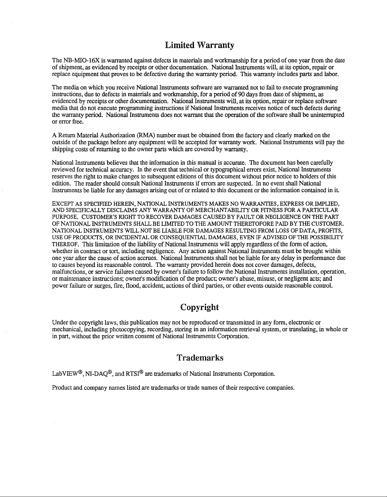
Limited
Warranty
The NB-MI0-16X is warranted against defects in materials and workmanship
of
shipment,
replace equipment that proves
The media on which you receive National Instruments software are warranted not to fail
instructions, due
evidenced by receipts or other documentation. National Instruments will, at its option, repair or replace software
media that
the warranty period. National Instruments does not warrant that the operation of the software shall be uninterrupted
or error
A Return Material Authorization
outside of the package before
shipping costs
National Instruments believes that
reviewed for technical accuracy.
reserves the right
edition. The reader should consult National Instruments
Instruments be liable for
EXCEPT
AND
SPECIFICALLY
PURPOSE.
OF
NATIONAL
NATIONAL
USE
OF
THEREOF.
whether in contract or tort, including negligence.
one year after the cause of action accrues. National Instruments shall not be liable for
to
causes beyond its reasonable control. The warranty provided herein does not cover damages, defects,
malfunctions, or service failures caused by owner's failure
or maintenance instructions; owner's modification of the product; owner's abuse, misuse, or negligent acts; and
power failure or surges, fire, flood, accident, actions of third parties, or other events outside reasonable control.
as
evidenced by receipts or other documentation. National Instruments will,
to
be defective during
to
defects in materials and workmanship, for a period of 90
do
not execute programming instructions
free.
(RMA)
any
of
returning
to
AS
SPECIFIED
CUSTOMER'S
INSTRUMENTS
INSTRUMENTS
PRODUCTS,
This limitation of the liability of National Instruments will apply regardless of the
to
the owner parts which are covered by warranty.
make changes
any
damages arising out of or related
HEREIN,
DISCLAIMS
RIGHT
SHALL
WILL
OR
INCIDENT
In
NATIONAL
TO
number must be obtained
equipment
the
the event that technical or typographical errors exist, National Instruments
to
subsequent editions of this document without prior notice
ANY
RECOVER
NOT
AL
will
information
WARRANTY
BE
LlMITED
BE
LlABLE
OR
CONSEQUENTIAL
the
warranty period. This warranty includes parts and labor.
if
National Instruments receives notice of such defects during
be
accepted for warranty
in
this manual
if
errors are suspected.
INSTRUMENTS
OF
MERCHANT
DAMAGES
FOR
Any
CAUSED
TO
THE
AMOUNT
DAMAGES
action against National Instruments must be brought within
to
follow the National Instruments installation, operation,
from
is
accurate. The document has been carefully
to
this document or
MAKES
DAMAGES,
NOW
ABILITY
BY
RESULTING
for
a period of one year
at
its option, repair or
to
execute programming
days
from date of shipment,
the factory and clearly marked on the
work.
National Instruments will pay
In
no
event shall National
the
information contained in
ARRANTIES,
OR
FITNESS
FAULT
THERETOFORE
EVEN
OR
FROM
IF
EXPRESS
FOR
NEGLlGENCE
PAID
BY
LOSS
OF
ADVISED
OF
form
any
delay in performance
from
as
to
holders of this
OR
IMPLlED,
AP
ARTICULAR
ON
THE
THE
CUSTOMER.
DATA,
PRoms.
THE
POSSIBILITY
of
action,
the date
the
it
PART
due
Copyright
Under
the
copyright laws, this publication
mechanical, including photocopying, recording, storing
the
in part, without
prior written consent of National Instruments Corporation.
may
not be reproduced or transmitted
in
an
information retrieval system, or translating, in whole or
Trademarks
Lab
VIEW®,
Product and company names listed are trademarks or trade names
NI-DAQ®.
and
RTSI®
are trademarks of National Instruments Corporation.
in
any
form,
of
their respective companies.
electronic or
Page 5

Warning Regarding Medical and Clinical Use
of
National Instruments Products
National Instruments products are
for
use
suitable
medical
part of
the
medical
traditional medical safeguards, equipment, and procedures that are appropriate in the particular situation
serious injury or death should always continue
National Instruments products are
equipment used
in treatment and diagnosis of
or
clinical treatment can create a potential
user or application designer.
or
clinical treatment must
to
monitor or safeguard human health
not
designed
Any
be
performed
NOT
intended to be a substitute for
with
components
humans.
use
to be
Applications of National Instruments products involving
for
accidental injury caused
or application of National Instruments products
by
properly trained
used
and
and
testing intended
and
qualified medical personnel,
when
National Instruments products are being
any
form
safety
in
medical
or
to
ensure
by
product failure, or
of established process, procedure,
clinical treatment
a level of reliability
by
for
or involving
and
errors
all
to
prevent
used.
on
the
or
Page 6
Preface
This manual describes the mechanical and electrical aspects
information concerning its operation and programming. The NB-MI0-16X is a high-performance
multifunction analog, digital, and timing input/output
NB-MI0-16X
The
two 12-bit digital-to-analog converters (DACs) with voltage outputs, eight lines
I/0,
digital
required, you can use the AMUX-64T multiplexer board.
and three 16-bit counter/timer channels for timing
contains a 16-bit analog-to-digital converter (ADC) with up to
of
the NB-MI0-16X and contains
(I/0)
board for Macintosh NuBus computers.
16
analog inputs,
of
TIL-compatible
I/0.
If
additional analog inputs are
Organization of This Manual
TheNB-MI0-16X
" Chapter
kit, the optional software, and the optional equipment; and explains how to unpack the
NB-MI0-16X.
" Chapter 2, Configuration and Installation, explains board configuration, installation
NB-MI0-16X
and cable wiring.
" Chapter 3, Theory
explains the operation
1,
User Manual is organized as follows:
Introduction, describes the NB-MI0-16X; lists the contents
in the Macintosh NuBus computer, signal connections to the NB-MI0-16X,
of
Operation, contains a functional overview
of
each functional unit making up the NB-MI0-16X.
of
of
your NB-MI0-16X
the NB-MI0-16X and
of
the
" Chapter 4, Programming, describes in detail the address and function
NB-MI0-16X
NB-MI0-16X.
the
" Chapter 5, Calibration Procedures, discusses the calibration procedures for the NB-MI0-16X
analog input and analog output circuitry.
" Appendix A, Specifications, lists the specifications
" Appendix
I/0
connector.
" Appendix C,
AmZ8073A System Controller (Advanced Micro Devices, Inc.) integrated circuit. This circuit
is used on the NB-MI0-16X.
" Appendix D, Customer Communication, contains forms for you
communication with National Instruments concerning our products.
" The Index contains an alphabetical list
the page where each one can
registers. This chapter also includes important information about programming
of
the NB-MI0-16X.
B,
I/0
Connector, contains the pinout and signal names for the NB-MI0-16X 50-pin
AMD
Data Sheet, contains the manufacturer data sheet for the Am9513Af
of
key terms and topics used in this manual, including
be found.
of
each
of
the
to
complete to facilitate
©
National
Instruments
Corporation
V
NB-MI0-16X
User
Manual
Page 7
Preface
Conventions Used
The
following conventions are used in this manual:
DIFF
DMAboard
italic
Macintosh
NI-DAQ
NRSE
RSE
DIFF refers to differential input configuration.
DMA
unless otherwise noted.
Italic text denotes emphasis, a cross reference,
concept.
Macintosh refers to
unless otherwise noted.
NI-DAQ is used throughout this manual to refer to the NI-DAQ software for
Macintosh unless otherwise noted.
NRSE
RSE refers to referenced single-ended input configuration.
in
This Manual
board refers to the NB-DMA-8-G board
refers to non-referenced single-ended input configuration.
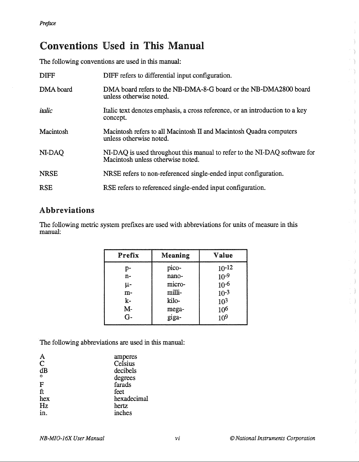
Abbreviations
or
the NB-DMA2800 board
or
an introduction
to a key
all Macintosh II and Macintosh Quadra computers
The
following metric system prefixes are used with abbreviations for units
manual:
Prefix
pn- nano-
µ-
m-
k-
M-
G-
The
following abbreviations are used in this manual:
A amperes
C
dB
0
F
ft
hex hexadecimal
Hz
in.
Celsius
decibels
degrees
farads
feet
hertz
inches
Meaning
pico-
micro-
milli-
kilomegagiga-
Value
10-12
10-9
lQ-6
10-3
103
106
109
of
measure
in
this
NB-MI0-16X
User
Manual
vi
©
National
Instruments
Corporation
Page 8
Preface
Abbreviations
m
M
.Q
(continued)
%
ppm
rms
sec
V
Vrms
Acronyms
The following acronyms
AC
ND
AOC
CMOS
DIA
DAC
DMA
EPROM
FIFO
I/0
LSB
NMR
ROM
RTSI
TC
TIL
VDC
VI
meters
megabytes of memory
ohms
percent
parts per million
mean
root
square
seconds
volts
volts root mean square
are
used in this
manual:
alternating current
analog-to-digital
AID
converter
complementary metallic oxide semiconductor
digital-to-analog
DI A converter
direct
memory
access
electrical programmable read-only memory
first-in-first-out
input/output
least significant bit
nonmaskable interrupt request
read-only memory
Real-Time
System
Integration
terminal count
transistor-transistor logic
volts direct current
virtual instrument
Related Documentation
The following documents contain information that you
• The Macintosh II or Quadra Owner's Manual, Getting Started manual, or Setting
if
you
plan
to
Consult the following manual
NB-MI0-16X:
• The Am9513A/Am9513 System Timing Controller technical manual
©
National
Instruments
Corporation
program the Am9513A Counter!fimer
vii
may
find helpful
as
you
NB-MJ0-16X
read
this manual:
Up
manual
used
on
the
User
Manual
Page 9
Preface
Consult the following National Instruments manuals
if
you plan to program
DMA
operations with
this board:
0
The
NB-DMA-8-G User Manual (part number 320097-01)
0
The
NB-DMA2800 User Manual (part number 320240-01)
Customer Communication
National Instruments wants to receive your comments on our products and manuals.
interested in the applications you develop with our products, and we want to help
problems with them. To make it easy for you to contact us,
this
manual contains comment and
configuration forms for you to complete. These forms are in Appendix D, Customer
Communication,
at the end
of
this
manual.
if
you have
We
are
NB-MI0-16X
User
Manual
viii
© National
Instruments
Corporation
Page 10
Contents
Chapter 1
Introduction
What Your Kit Should Contain ...................................................................................... 1-3
Optional Software .......................................................................................................... 1-4
Optional Equipment ....................................................................................................... 1-4
Unpacking ...................................................................................................................... 1-5
Chapter 2
Configuration
Board Configuration ...................................................................................................... 2-1
Jumper Settings .............................................................................................................. 2-1
Analog Input Configuration ........................................................................................... 2-4
Analog Output Configuration ........................................................................................ 2-9
Installation ...................................................................................................................... 2-13
Signal Connections ........................................................................................................ 2-13
..........................................................................................................................
and
Input Mode ......................................................................................................... 2-4
Input Polarity and Input Range .......................................................................... 2-7
External and Internal Reference ......................................................................... 2-9
Analog Output Polarity Selection ...................................................................... 2-10
Analog Input Signal Connections ...................................................................... 2-14
Types
Input Configurations .......................................................................................... 2-16
Analog Output Signal Connections .................................................................... 2-22
Digital
Power Connections ............................................................................................ 2-25
Timing Connections ........................................................................................... 2-26
1-1
Installation
DIFF Input
RSE Input (16 Channels) ....................................................................... 2-5
NRSE Input (16 Channels) .................................................................... 2-6
Considerations for Selecting Input Ranges ............................................ 2-7
External Reference Selection ................................................................. 2-9
Internal Reference Selection (Factory Setting) ...................................... 2-9
Bipolar Output Selection (Factory Setting) ........................................... 2-10
Straight Binary Mode ................................................................. 2-11
Two's Complement Mode (Factory Setting) .............................. 2-11
Unipolar Output Selection ..................................................................... 2-12
of
Signal Sources ..................................................................................... 2-16
Floating Signal Sources ......................................................................... 2-16
Ground-Referenced Signal Sources ....................................................... 2-16
Differential Connection Considerations (DIFF Configuration) ............. 2-17
Differential Connections for Grounded Signal Sources ........................ 2-17
Differential Connections for Floating Signal Sources ........................... 2-18
Single-Ended Connection Considerations ............................................. 2-20
Single-Ended Connections for Floating Signal Sources
(RSE Configuration) .............................................................................. 2-20
Single-Ended Connections for Grounded Signal Sources
(NRSE Configuration) ........................................................................... 2-21
Common Mode Signal Rejection Considerations .................................. 2-21
I/0
Signal Connections .......................................................................... 2-23
Data Acquisition Timing Connections ................................................... 2-26
General-Purpose Timing Signal Connections ........................................ 2-28
.......................................................................................
(8
Channels, Factory Setting) ............................................. 2-4
2-1
©
National
Instruments
Corporation
ix
NB-MI0-16X
User
Manual
Page 11
Contents
Cabling and Field Wiring ............................................................................................... 2-32
Field Wiring Considerations .............................................................................. 2-32
Cabling Considerations ...................................................................................... 2-33
Chapter 3
Theory of Operation
Functional Overview ...................................................................................................... 3-1
NuBus Interface Circuitry .............................................................................................. 3-2
Analog Input and
Analog
Data
Analog Output Circuitry ................................................................................................. 3-8
Digital
Timing
RTSI Bus Interface Circuitry ......................................................................................... 3-13
I/0
J/0 Circuitry ...................................................................................................... 3-11
In~u~
Acqu1s1tton TlIIlmg Crrcmtry .................................................................... 3-6
Single-Channel Data Acquisition .......................................................... .3-7
Multiple-Channel (Scanned) Data Acquisition ..................................... .3-7
Circuitry ....................................................................................................... 3-9
Chapter 4
Programming
Register Access .............................................................................................................. 4-1
Register Description ....................................................................................................... 4-3
........................................................................................................................
Slot Address Space ............................................................................................. 4-1
Register Map ...................................................................................................... 4-2
Register Sizes ..................................................................................................... 4-3
Register Description Format .............................................................................. 4-4
Configuration and Status Register Group ......................................................... .4-5
Status Register ........................................................................................ 4-6
Command Register 1 .............................................................................. 4-8
Command Register 2 .............................................................................. 4-11
The
Event Strobe Register Group ..................................................................... .4-13
Start Convert Register ............................................................................ 4-14
Start
AID
External Multiplexer Strobe Register .................................................... .4-17
Internal Calibration Register .................................................................. 4-18
Analog Output Register Group .......................................................................... 4-19
DACO,
TMRINTCL Register ............................................................................. 4-21
Analog Input Register Group ............................................................................. 4-22
Mux-Counter Register ............................................................................ 4-23
Mux-Gain Register ................................................................................. 4-24
AID
Arn9513A Counter/fimer Register Group ........................................................ .4-27
Arn9513A Data Register ........................................................................ 4-28
Arn9513A Command Register .............................................................. .4-29
Arn9513A Status Register ...................................................................... 4-30
Digital
The
I/0
Digital Input Register ............................................................................. 4-32
Digital Output Register .......................................................................... 4-33
RTSI Switch Register Group ...................................................................... 4-34
RTSI Switch Shift Register .................................................................... 4-35
RTSI Switch Strobe Register ................................................................. 4-36
...........................................................................................................
Data
Acquisition Circuitry ............................................................... .3-3
~ircu.it:rr ·······:·····:·········································································3-5
DAQ
Clear Register ................................................................................. 4-16
FIFO Register ................................................................................. 4-26
Register Group ................................................................................. 4-31
Register ................................................................................ 4-15
DACl
Registers ......................................................................... 4-20
3-1
4-1
NB-MI0-16X
User
Manual
X
© National Instruments
Corporation
Page 12
Contents
The Configuration EPROM ........................................................................................... 4-37
Programming Considerations ......................................................................................... 4-38
Register Programming Considerations ............................................................. .4-38
Initializing the NB-MI0-16X Board ................................................................. .4-38
Initializing the RTSI Bus Switch .......................................................... .4-39
Initializing the Am9513A ...................................................................... 4-39
Performing an Internal ADC Calibration .............................................. .4-40
Initializing the Analog Output Circuitry ............................................... .4-41
Programming the Analog Input Circuitry ......................................................... .4-41
1.
Select analog input channel and gain ............................................... .4-41
2.
Initiate an
3. Read the
ND
FIFO Output Binary Formats ........................................................ .4-42
ND
conversion ................................................................ 4-41
ND
conversion result ....................................................... .4-42
Clearing the Analog Input Circuitry ..................................................... .4-44
Programming Multiple
1.
Select analog input channel and gain ............................................... .4-45
2.
Program the sample-interval counter ................................................ 4-45
ND
Conversions on a Single Input Channel .............. .4-44
3. Program the sample counter .............................................................. 4-46
Sample Counts 2 through 65,536 .............................................. .4-46
Sample Counts Greater than 65,536 ......................................... .4-47
4. Clear the
ND
circuitry ...................................................................... 4-48
5. Enable the data acquisition operation .............................................. .4-48
6.
Apply a trigger .................................................................................. 4-48
7. Service the data acquisition operation ............................................. .4-48
External Timing Considerations for Multiple
ND
Conversions ...................... .4-49
Pretriggering with the STOPTRIG Signal ............................................ .4-49
1.
Select analog input channel and gain .................................... 4-50
2.
Program the sample-interval counter ................................... .4-50
3.
Program the sample counter ................................................. .4-51
Sample Counts 2 through 65,536 ................................ .4-51
Sample Counts Greater than 65,536 ............................. .4-51
4.
Clear the
ND
circuitry .......................................................... 4-52
5. Apply a trigger ...................................................................... 4-52
6.
Service the data acquisition operation ................................. .4-53
Controlling Multiple
ND
Conversions
with the EXTCONV* Signal ................................................................ .4-54
1.
Select analog input channel and gain ................................... .4-54
2.
Clear the
3.
Service the data acquisition operation ................................. .4-54
Programming Multiple
Multiple
ND
ND
circuitry .......................................................... 4-54
ND
Conversions with Channel Scanning ................... .4-55
Conversions with Continuous Channel Scanning
(Round-Robin) ....................................................................................... 4-56
1.
Set up the analog channel and gain selection sequence ....... .4-56
2.
Program the sample-interval counter ................................... .4-57
3.
Program the sample counter ................................................. .4-58
Sample Counts 2 through 65,536 .................................. .4-58
Sample Counts Greater than 65,536 ............................. .4-58
4.
Clear the
ND
circuitry and reset the mux counter .............. .4-59
5. Enable the scanning data acquisition operation ................... .4-59
6.
Apply a trigger ...................................................................... 4-60
7. Service the data acquisition operation ................................. .4-60
Multiple
ND
Conversions with Interval Channel Scanning (Pseudo-
Simultaneous) ......................................................................................... 4-61
1.
Set up the analog channel and gain selection sequence ....... .4-61
@ National Instruments
Corporation
xi
NB-MI0-16X User Manual
Page 13
Contents
2. Program the sample-interval counter ................................... .4-62
3. Program the sample counter ................................................. .4-63
Sample Counts 2 through 65,536 .................................. .4-63
Sample Counts Greater than 65,536 ............................. .4-64
4. Program the scan-interval counter ....................................... .4-65
5. Clear the
6.
Enable the scanning data acquisition operation ................... .4-66
7. Apply a trigger ...................................................................... 4-66
8.
Service the data acquisition operation ................................. .4-66
External Timing Considerations for Scanned Data Acquisition ........... .4-67
Resetting the Hardware after a Data Acquisition Operation ............................. .4-68
Resetting Counter 2 ................................................................................ 4-68
Resetting Counter 3 ................................................................................ 4-68
Resetting Counter 4 ................................................................................ 4-69
Resetting Counter 5 ................................................................................ 4-69
Programming the Analog Output Circuitry ...................................................... .4-70
Programming the Digital
Programming the Am9513A Counter!fimer .................................................... .4-73
RTSI Bus Trigger Line Programming Considerations ..................................... .4-73
NB-MI0-16X RTSI Signal Connection Considerations ...................... .4-74
Programming the RTSI Switch ............................................................. .4-75
Programming
Interrupt Programming ....................................................................................... 4-77
DMA
Operations ........................................................................ .4-76
ND
circuitry and reset the mux counter .............. .4-66
I/0
Circuitry ............................................................. .4-72
Chapter
5
Calibration Procedures
Calibration Equipment Requirements ............................................................................ 5-1
Calibration Trimpots ...................................................................................................... 5-2
Analog Input Calibration ............................................................................................... 5-3
Sample Averaging .............................................................................................. 5-3
Board Configuration .......................................................................................... 5-3
Bipolar Input Calibration Procedure .................................................................. 5-4
Unipolar Input Calibration Procedure ................................................................ 5-5
Analog Output Calibration ............................................................................................. 5-6
Board Configuration .......................................................................................... 5-6
Bipolar Output Calibration Procedure ............................................................... 5-7
Unipolar Output Calibration Procedure ............................................................. 5-8
Appendix A
Specifications
Analog Input ..................................................................................................................
Analog Data Acquisition Rates ...................................................................................... A-3
Analog Output ................................................................................................................ A-4
Digital
Timing
Power Requirement (from NuBus) ................................................................................ A-5
Physical .......................................................................................................................... A-5
Operating Environment .................................................................................................. A-5
Storage Environment. ..................................................................................................... A-5
........................................................................................................................
Explanation
Single-Channel Acquisition Rates ..................................................................... A-3
Multiple-Channel Acquisition Rates .................................................................. A-3
Explanation
I/0
...................................................................................................................... A-4
I/0
...................................................................................................................... A-5
of
of
.....................................................................................................
Analog Input Specifications ...................................................... A-2
Analog Output Specifications ................................................... A-4
5-1
A-1
A-1
NB-MI0-16X
User
Manual xii
© National Instruments
Corporation
Page 14
AppendixB
1/0
Connector
.......................................................................................................................
Appendix C
AMD Data Sheet
..................................................................................................................
AppendixD
Customer Communication
Contents
..............................................................................................
B-1
C-1
D-1
Index
Figure 1-1.
Figure 2-1.
Figure 2-2.
Figure 2-3.
Figure 2-4.
Figure 2-5.
Figure 2-6.
Figure 2-7.
Figure 2-8.
Figure 2-9.
Figure 2-10.
Figure 2-11.
Figure 2-12.
Figure 2-13.
Figure 2-14.
Figure 2-15.
Figure 2-16.
Figure 2-17.
Figure 2-18.
Figure 2-19.
Figure 2-20.
Figure 2-21.
Figure 2-22.
Figure 2-23.
Figure 2-24.
Figure 2-25.
Figure 2-26.
Figure 2-27.
Figure 2-28.
..................................................................................................................................
Index-I
Figures
NB-MI0-16X Interface Board ........................................................................... 1-2
Parts Locator Diagram ....................................................................................... 2-3
DIFF Input Configuration (Factory Setting) ...................................................... 2-5
RSE Input Configuration ................................................................................... 2-6
NRSE Input Configuration ................................................................................. 2-6
5 V Input Configuration ..................................................................................... 2-7
.2-
10 V Input Configuration (Factory Setting) ......................................................
External Reference Configuration ..................................................................... 2-9
Internal Reference Configuration (Factory Setting) .......................................... 2-10
Reference Choice Configurations ...................................................................... 2-10
Bipolar Output Configuration (Factory Setting) ................................................
Straight Binary Mode .........................................................................................
Two's Complement Mode (Factory Setting) ...................................................... 2-12
Unipolar Output Configuration .......................................................................... 2-12
NB-MI0-16X
NB-MI0-16X Instrumentation Amplifier .......................................................... 2-15
Differential Input Connections for Grounded Signal Sources ........................... 2-18
Differential Input Connections for Floating Sources ......................................... 2-19
Single-Ended Input Connections for Floating Signal Sources ........................... 2-20
Single-Ended Input Connections for Grounded Signal Sources ........................ 2-21
Analog Output Connections ............................................................................... 2-23
Digital
EXTSTROBE* Signal Timing ........................................................................... 2-26
EXTCONV* Signal Timing ............................................................................... 2-27
STARTTRIG* Signal Timing ............................................................................ 2-27
STOPTRIG Signal Timing ................................................................................. 2-28
Event-Counting Application with External Switch Gating ................................ 2-29
Frequency Measurement Application ................................................................ 2-30
General-Purpose Timing Signals ....................................................................... 2-31
I/0
I/0
Connector ............................................................................. 2-14
Connections ..................................................................................... 2-25
7
2-11
2-11
Figure 3-1.
Figure 3-2.
Figure 3-3.
Figure 3-4.
Figure 3-5.
Figure 3-6.
© National
Instruments
NB-MI0-16X Block Diagram ........................................................................... 3-1
NuBus Interface Circuitry Block Diagram ........................................................ 3-2
Analog Input and Data Acquisition Circuitry Block Diagram ......................... .3-4
Analog Output Circuitry Block Diagram ........................................................... 3-8
I/0
Digital
Timing
Circuitry Block Diagram ................................................................ .3-10
I/0
Circuitry Block Diagram ................................................................ .3-11
Corporation
xiii NB-MI0-16X
User
Manual
Page 15
Contents
Figure 3-7.
Figure 3-8.
Figure 4-1.
Figure 5-1.
Figure B-1.
Table
2-1.
Table 2-2.
Table
Table
2-3.
2-4.
Table 4-1.
Table
Table
Table
Table
Table
Table
Table
Table
4-2.
4-3.
4-4.
4-5.
4-6.
4-7.
4-8.
4-9.
Counter Block Diagram ..................................................................................... 3-12
RTSI Bus Interface Circuitry Block Diagram .................................................... 3-14
RTSI Switch Control Pattern ............................................................................. 4-75
Calibration Trimpot Location Diagram ............................................................. 5-2
NB-MI0-16X
I/0
Connector ............................................................................. B-1
Tables
Jumper Settings .................................................................................................. 2-2
Input Configurations Available for the NB-MI0-16X ...................................... 2-4
Actual Range and Measurement Precision Versus Input Range
Selection and Gain ............................................................................................. 2-8
Recommended Input Configurations for Ground-Referenced
and Floating Signal Sources ............................................................................... 2-17
Macintosh Slot Addresses .................................................................................. 4-2
NB-MI0-16X Register Map .............................................................................. 4-3
Straight Binary Mode
Two's Complement Mode
Single-Channel Data Acquisition Rates ............................................................ .4-49
Multiple-Channel Data Acquisition Rates ........................................................ .4-67
Analog Output Voltage Versus Digital Code (Unipolar Mode) ....................... .4-71
Analog Output Voltage Versus Digital Code (Bipolar Mode) ......................... .4-72
RTSI Switch Signal Connections ...................................................................... .4-74
ND
Conversion Values ................................................ .4-43
ND
Conversion Values .......................................... .4-43
NB-MI0-16X
User
Manual
xiv
© National
Instruments
Corporation
Page 16

Chapter 1
Introduction
This chapter describes the
software, and
The
NB-MI0-16X
Macintosh
•
Fast
Programmable
42
Guaranteed rates up to 55 ksamples/sec
Internal or external
"
Two
Unipolar and bipolar voltage output available
Onboard reference voltages
the
optional equipment; and explains
is a high-perfonnance multifunction analog, digital and timing
NuBus
16-bit
16 single-ended or 8 differential channels (expandable with AMUX-64T multiplexer board)
µsec converter
16-word
double-buffered multiplying 12-bit
computers.
ADC
FIFO
gains
ND
NB-MI0-16X;
The
NB-MI0-16X
of
1, 10,
or
18 µsec converter
buffer to obtain the highest possible data acquisition rate
ND
timing
of
lists the contents
has
100,500,
5 V and 10 V
or
DACs
how
to unpack the
the
following features:
1, 2, 4, 8
of
your
NB-MI0-16X
NB-MI0-16X.
kit, the optional
J/0
board for
Onboard timer for wavefonn generation
• Eight digital
• Three independent 16-bit counter/timers for frequency counting, event counting,
output applications
" Timer-generated interrupts
• High-perfonnance
Triggers for system-level timing
DMA
©
National
Instruments
J/0
lines,
each
able to sink up to
RTSI
bus interface
operation over a RTSI bus with a
Corporation
24
mA
DMA
1-/
current
board
NB-M/0-16X
and
pulse
User
Manual
Page 17
Introduction
Chapter
1
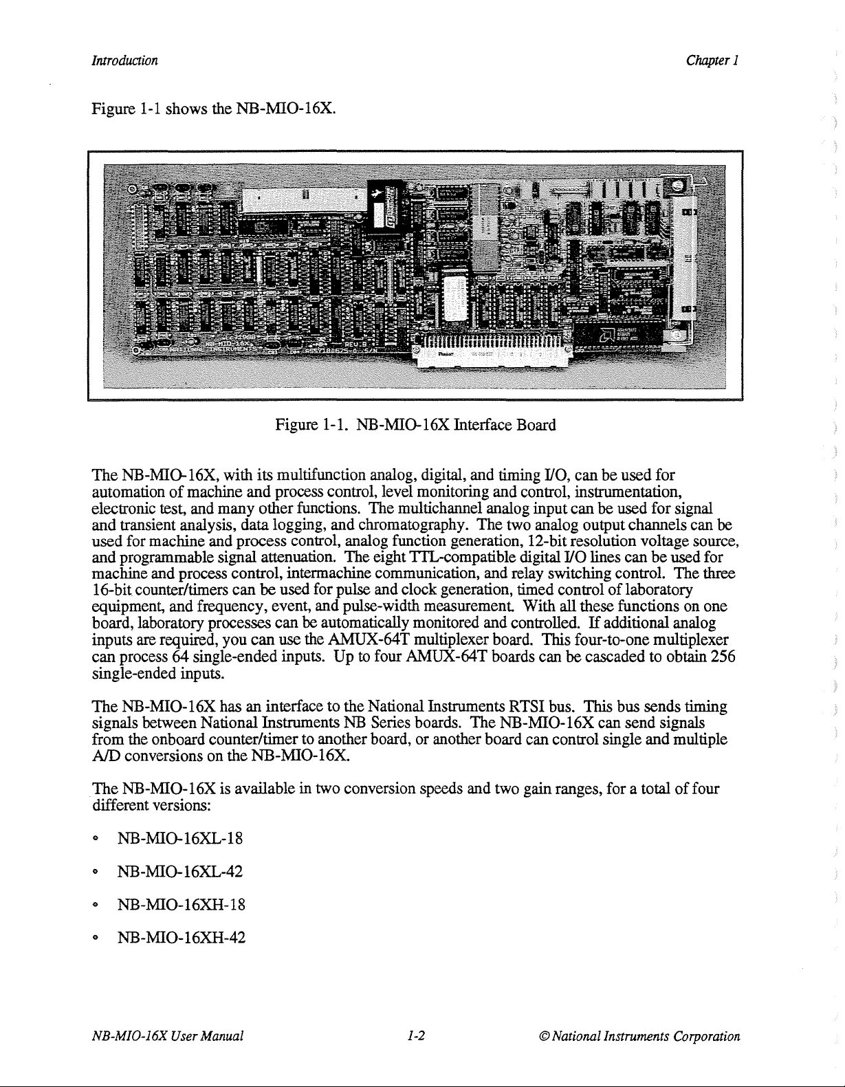
Figure
1-1
shows the
NB-MI0-16X.
Figure 1-1. NB-MI0-16X Interface Board
The
NB-MI0-16X, with its multifunction analog, digital, and timing
automation
of
machine and process control, level monitoring and control, instrumentation,
electronic test, and many other functions. The multichannel analog input can
I/0,
can be used for
be used for signal
and transient analysis, data logging, and chromatography. The two analog output channels can be
used for machine and process control, analog function generation, 12-bit resolution voltage source,
I/0
and programmable signal attenuation. The eight TTL-compatible digital
machine and process control, intermachine communication, and relay switching control. The
16-bit counter/timers can be used for pulse and clock generation, timed control
lines can be used for
three
of
laboratory
equipment, and frequency, event, and pulse-width measurement. With all these functions on one
board, laboratory processes can be automatically monitored and controlled.
If
additional analog
inputs are required, you can use the AMUX-64T multiplexer board. This four-to-one multiplexer
can process
64
single-ended inputs.
Up
to
four AMUX-64T boards can be cascaded to obtain 256
single-ended inputs.
The
NB-MI0-16X has an interface to the National Instruments RTSI bus. This bus sends timing
signals between National Instruments NB Series boards. The NB-MI0-16X can send signals
from the onboard counter/timer to another board, or another board can control single and multiple
AID conversions on the NB-MI0-16X.
The
NB-MI0-16X is available in two conversion speeds and two gain ranges, for a total
of
four
different versions:
• NB-MI0-16XL-18
• NB-MI0-16XL-42
• NB-MI0-16XII-18
• NB-MI0-16XII-42
NB-MI0-16X
User
Manual
1-2
© National Instruments
Corporation
Page 18
Chapter
The
analog input signals. The NB-MI0-16XH
and 8 for high-level analog input signals. The
µsec
capable
I
NB-MI0-16XL
conversion rate, which is about 24 kbytes/sec. The NB-MI0-16X(L/H)-18 has an ADC
of
an 18
has software-programmable gain settings
has software programmable gain settings
NB-MI0-16X(LJH)-42 has an ADC capable
µsec
conversion rate, which is about 55 kbytes/sec.
of
1, 10, 100, and 500 for low-level
Introduction
of
1, 2, 4,
of
a 42
Detailed specifications for the NB-MI0-16X are included
What
Each version
follows.
Kit
Your
of
Name
Kit Should Contain
the NB-MI0-16X board has a different part number and kit part number, listed as
Kit
Part
Number
in
Appendix A, Specifications.
Kit
Component
Board
Part
Number
NB-MI0-16XL-18
NB-MI0-16XL-42 776259-02
NB-MI0-16XH-18
NB-MI0-16XH-42
The board part number is printed on your board along the top edge on the component side. You
can identify which version
the preceding table.
776259-01 NB-MI0-16XL-18 board 180675-01
NB-MI0-16XL-42 board 180675-02
776259-11
776259-12 NB-MI0-16XH-42 board
of
the NB-MI0-16X board you have by looking up the part number in
NB-MI0-16XH-18 board
180675-11
180675-12
In addition to the board, each version
Kit
NB-MI0-16X
NI-DAQ software for Macintosh, with manuals 776181-01
NI-DAQfor Macintosh Software Reference Manual 320103-01
If
your kit is missing any
Instruments.
Your
NB-MI0-16X
of
functions that can be called from your application programming environment These functions
include routines for analog input
conversion), analog output (D/A conversion), waveform generation, digital
SCXI, RTSI, and self-calibration. NI-DAQ maintains a consistent software interface among its
different versions so you can switch between platforms with minimal modifications to your code.
NI-DAQ comes with language interfaces for MPW C,
QuickBASIC. Any language that uses Device Manager Toolbox calls can access NI-DAQ.
User Manual 320157-01
of
the components or
is shipped with the NI-DAQ software for Macintosh. NI-DAQ has a library
of
the NB-MI0-16X kit contains the following components.
Component
if
you received the wrong version, contact National
(ND
conversion), buffered data acquisition (high-speed
THINK
C, Pascal, and Microsoft
Part
I/0,
Number
ND
counter/timer,
©
NaJi.onal
lnstrwnents
CorporaJion
1-3
NB-MI0-16X
User
Manual
Page 19
Introduction
Chapter
Optional Software
This manual contains complete instructions for directly programming the NB-MI0-16X.
to
Normally, however, you should not need
manual because the NI-DAQ software package for controlling the NB-MI0-16X is included with
the board. Using NI-DAQ is quicker and easier than and
programming described in Chapter 4,
read the low-level programming details in the user
as
flexible as using the low-level
Programming.
1
The NB-MI0-16X can also
be
used with Lab VIEW (part number 776141-01), a software system
that features interactive graphics, a state-of-the-art user interface, and a powerful graphical
programming language. The Lab VIEW Data Acquisition VI Library, a series of VIs
for
using
Lab VIEW with the NB-MI0-16X and other National Instruments boards, is included with
Lab
VIEW.
The
Lab
VIEW Data Acquisition VI Library
is
functionally equivalent
to
the
NI-DAQ
software for Macintosh.
Optional
NB-DMA2800 board
NB-DMA-8-G board
CB-50
NB
I/0
with 0.5-m
with 1.0-m
Series R TSI bus cables for
Equipment
connector block
type
NB
1 cable
type
NB
1 cable
Equipment
(50
screw terminals)
Part
Number
776305-01
776161-01
776164-01
776164-02
2 boards 776188-02
3 boards
4 boards
5 boards
776188-03
776188-04
776188-05
SCXI signal conditioning modules
SCXI-1100 32-channel differential multiplexer/ amplifier
SCXI-1120 8-channel isolated analog input
SCXI-1121 4-channel isolated transducer amplifier with excitation 776572-21
SCXI-1140 8-channel simultaneously sampling differential amplifier
SCXI-1180 feedthrough panel
SCXI-1181 breadboard
AMUX-64T analog multiplexer board
with 0.2-m ribbon cable
with 0.5-m ribbon cable
with 1.0-m ribbon cable
with 2.0-m ribbon cable
NB-MI0-16X
User
Manual
1-4
©
National
Instruments
776572-00
776572-20
776572-40
776572-80
776572-81
776366-02
776366-05
776366-10
776366-20
(continues)
Corporation
Page 20
Chapter
1
Introduction
Equipment
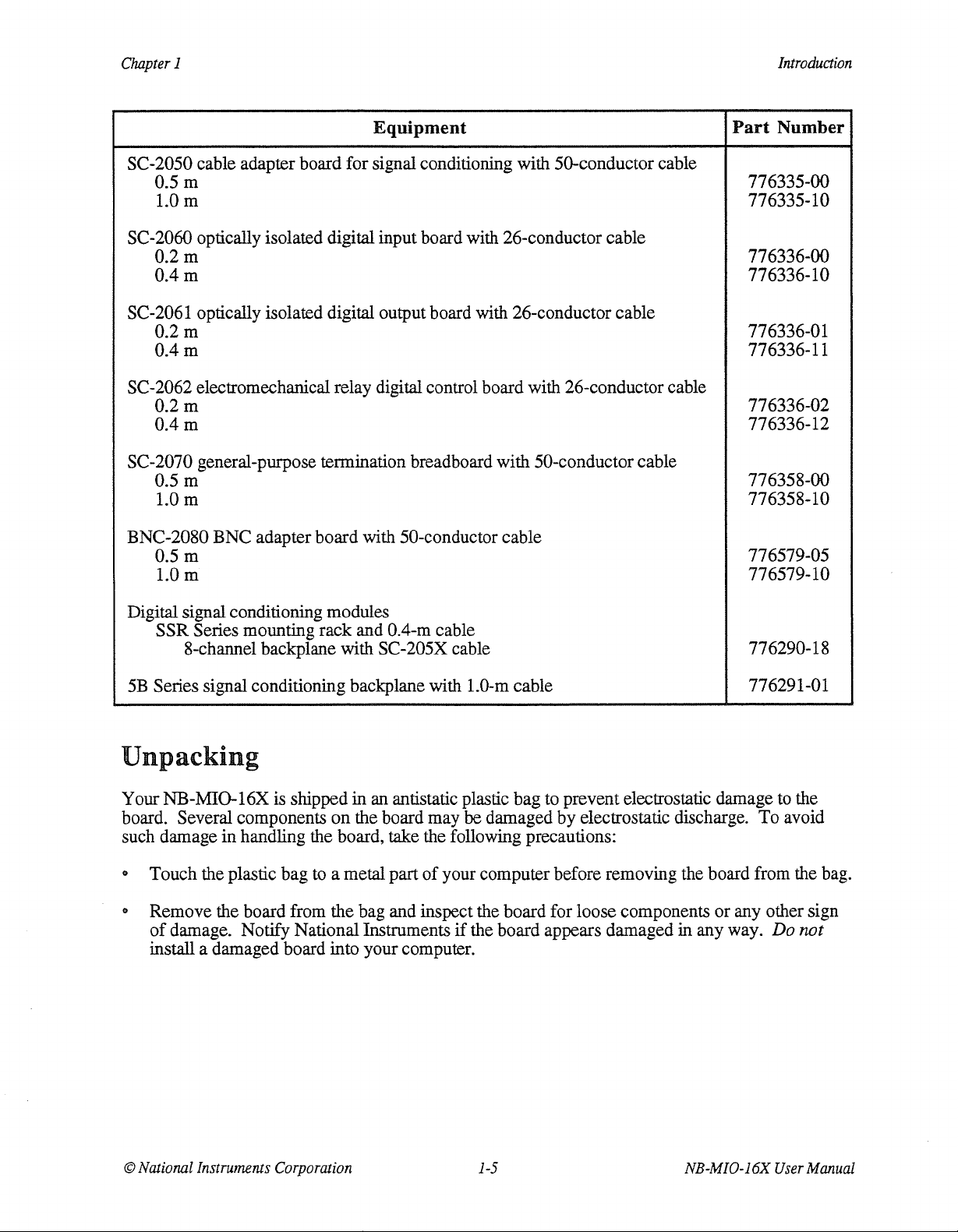
SC-2050 cable adapter board for signal conditioning with 50-conductor cable
0.5m
1.0 m
SC-2060 optically isolated digital input board with 26-conductor cable
0.2m
0.4m
SC-2061 optically isolated digital output board with 26-conductor cable
0.2m
0.4m
SC-2062 electromechanical relay digital control board with 26-conductor cable
0.2m
0.4m
SC-2070 general-purpose termination breadboard with 50-conductor cable
0.5m
1.0 m
BNC-2080 BNC adapter board with 50-conductor cable
0.5m
1.0 m
Part Number
776335-00
776335-10
776336-00
776336-10
776336-01
776336-11
776336-02
776336-12
776358-00
776358-10
776579-05
776579-10
Digital signal conditioning modules
SSR Series mounting rack and 0.4-m cable
8-channel backplane with SC-205X cable
5B
Series signal conditioning backplane with 1.0-m cable
776290-18
776291-01
Unpacking
Your NB-MI0-16X is shipped in an antistatic plastic bag to prevent electrostatic damage
on
board. Several components
such damage in handling the board, take the following precautions:
• Touch the plastic bag
• Remove the board from the bag and inspect the board for loose components or any other sign
of
damage. Notify National Instruments
install a damaged board into your computer.
the board may be damaged by electrostatic discharge. To avoid
to
a metal part
of
your computer before removing the board from the bag.
if
the board appears damaged in any way. Do
to
the
not
© National Instruments Corporation
1-5
NB-MI0-16X
User
Manual
Page 21

Chapter
2
Configuration
This chapter explains board configuration, installation
NuBus computer, signal connections to the NB-MI0-16X,
and
Installation
of
the NB-MI0-16X in the Macintosh
and
cable wiring.
Board Configuration
The NB-MI0-16X has 10 jumpers that determine the analog input and analog output
configurations
Jumpers W3, W5, and
W9, and WlO configure the analog output circuitry.
of
the board. The jumpers are shown in the parts locator diagram in Figure 2-1.
W8
configure the analog input circuitry. Jumpers
Wl,
W2, W4, W6, W7,
Jumper Settings
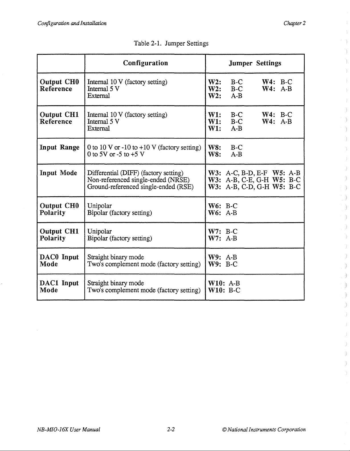
The NB-MI0-16X is shipped from the factory with the following configuration:
• Differential analog input
•
10
V input range
• ±10 V output range with internal 10 V reference selected
(8
channels)
" Two's complement
Table 2-1 lists all the available jumper configurations for the NB-MI0-16X with the factory
settings noted.
DAC
input mode
©
National
Instruments Corporation
2-1
NB-MI0-16X
User
Manual
Page 22
Configuration
and
Installation
Table 2-1. Jumper Settings
Chapter
2
Output
CHO Internal
Reference
Output
CHl
Reference
Input
Input
Output
Range
Mode
CHO Unipolar
Polarity
Configuration
10
V (factory setting)
Internal 5 V
External
Internal
10
V (factory setting)
Internal 5 V
External
0 to 10 V or -10 to +
-5
0 to 5V or
to
+5
10
V (factory setting)
V
Differential (DIFF) (factory setting)
Non-referenced single-ended (NRSE)
Ground-referenced single-ended (RSE)
Bipolar (factory setting)
W2:
W2:
W2:
Wl:
WI:
Wl:
WS:
WS:
W3:
W3:
W3:
W6:
W6:
Jumper
B-C
B-C
Settings
W4:
W4:
B-C
A-B
A-B
B-C
B-C
W4:
W4:
B-C
A-B
A-B
B-C
A-B
A-C, B-D, E-F WS: A-B
A-B, C-E, G-H WS: B-C
A-B, C-D, G-H WS: B-C
B-C
A-B
Output
Polarity
DACO
Mode
DACI
Mode
CHI
Input
Input
Unipolar
Bipolar (factory setting)
Straight binary mode
Two's complement mode (factory setting)
Straight binary mode
Two's complement mode (factory setting)
W7:
W7:
W9:
W9:
WIO:
WIO:
B-C
A-B
A-B
B-C
A-B
B-C
NB-MI0-16X
User
Manual
2-2
© National Instruments
Corporation
Page 23
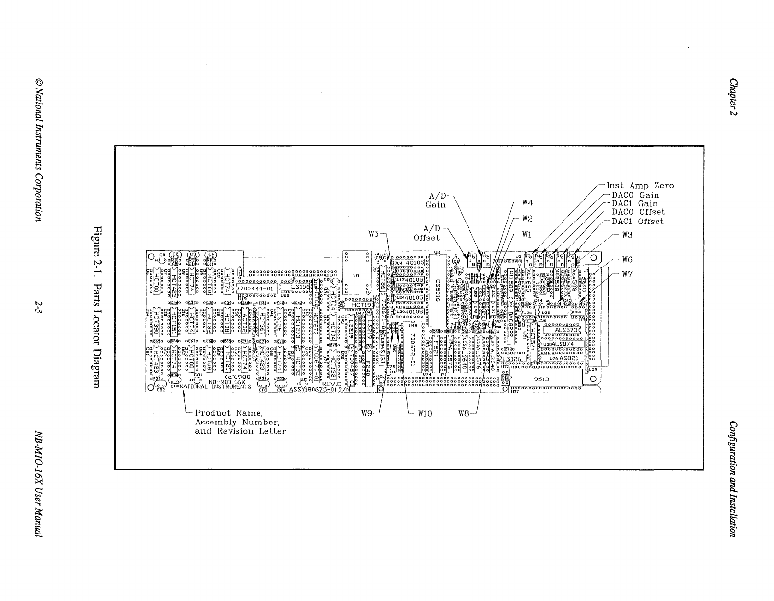
@
~
c3·
is
....
;;'
~
i
~
g
'g
g
c3·
:;:,i
"Tl
.....
(1Q
~
N
I
......
'1j
A/D-
Gain
-W'1
-W6
i
~
.....
tv
tv
~
&3
~
9
.._
~
~
.....
"'
f
i.:
e..
a
~
~
g
Cl
.....
~
~
W10
W8--
g
'Si
OQ
i.:
~
is·
:;:,i
l
a
s
~
c3·
:;:,i
Page 24
Configuration
and
Installation
Chapter2
Analog
You can select different analog input configurations
Table 2-1. The following paragraphs describe each
configuration illustrations throughout
Input
Configuration
this chapter, the black bars show where to place jumpers.
Input Mode
The
NB-MI0-16X
referenced single-ended (NRSE) input,
configurations use 16 channels. The
configurations
Configuration
offers three different input modes-referenced single-ended (RSE) input, non-
and
differential (DIFF)
DIFF
input configuration uses 8 channels. These
are
described
Table 2-2. Input Configurations Available for the
DIFF
RSE
in
Table 2-2.
Differential configuration.
Provides
the instrumentation amplifier tied to the multiplexer output
of
Channels 8 through 15.
Referenced Single-Ended configuration.
Provides 16 single-ended inputs with the negative (-) input
of
the instrumentation amplifier referenced to analog
ground.
8 differential inputs with the negative(-) input
by
using the jumper settings shown in
of
the analog input categories in detail.
input
The single-ended input
NB-MI0-16X
Description
of
In
the
NRSE
While reading the following paragraphs, you may find
Connections later
configurations.
DIFF Input
DIFF input means that each input signal has its own reference, and the difference between each
· signal and its reference is measured. The signal and its reference
channel. With
signals. You select the DIFF input configuration
W3:
in
this chapter, which contains diagrams showing the signal paths for the three
(8
Channels, Factory Setting)
this input configuration, the
A - C Jumper
together inside the board.)
B - D
AI
Non-Referenced Single-Ended configuration.
Provides 16 single-ended inputs with the negative(-) input
of
the instrumentation amplifier tied to AISENSE and not
connected
is placed
SENSE is tied
to
ground.
it
helpful to refer to
are
NB-MI0-16X
by
in
standby position. (A and C are always connected
to
the instrumentation amplifier signal ground.
can monitor eight different analog input
setting jumpers W3 and W5 as follows:
Analog
each assigned an input
Input Signal
NB-MJ0-16X.
User
Manual
24
©
National
I nstrwnents
Corporation
Page 25
Chapter
2
Configuratwn
andlnstallatwn
E-F
W5:
- B Multiplexer is configured to control eight input channels.
A
This configuration
Channels O through 7
instrumentation amplifier. Channels
(-) input
is
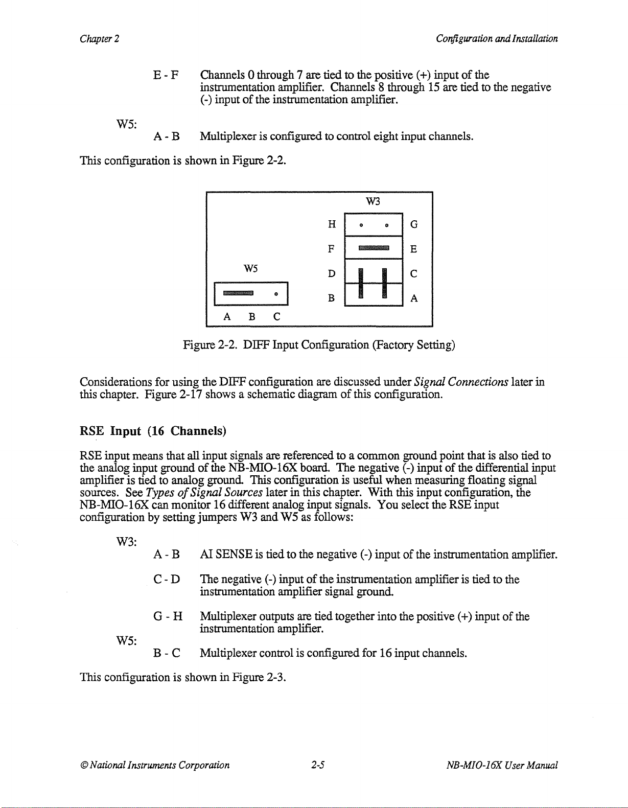
shown in Figure 2-2.
of
the instrumentation amplifier.
are
tied to the positive ( +) input
8 through
W3
H
F
"
..
G
E
15
-
W5
..
-
A
B C
Figure 2-2. DIFF Input Configuration (Factory Setting)
I
D
B
C
A
of
the
are
tied to the negative
Considerations for using the
this chapter. Figure 2-17 shows a schematic diagram
RSE Input (16 Channels)
RSE input means that all input signals
the analog input ground
is
amplifier
sources. See
NB-MI0-16X
configuration by setting jumpers
tied to analog ground. This configuration is useful when measuring floating signal
Types
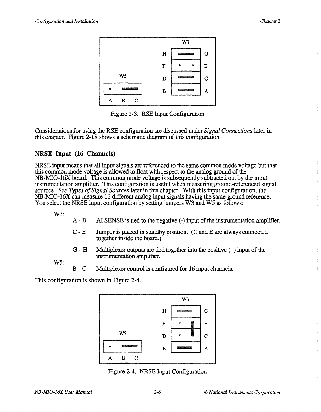
W3:
of
can monitor 16 different analog input signals.
A-B
C-D
G-H
W5:
B-C
This configuration
is
shown
DIFF
configuration are discussed under Signal Connections later in
are
referenced to a common ground point that is also tied to
of
the NB-MI0-16X board.
Signal
Sources
AI
SENSE is tied
The negative
instrumentation amplifier signal ground.
Multiplexer outputs
instrumentation amplifier.
Multiplexer control is configured for 16 input channels.
in
Figure 2-3.
W3
later
in
and
W5
to
(-) input
this chapter.
as
follows:
the negative (-) input
of
the instrumentation amplifier is tied to the
are
tied together into the positive ( +) input
of
this configuration.
The
negative(-) input
With
this input configuration, the
You
select the RSE input
of
the differential input
of
the instrumentation amplifier.
of
the
©
National
Instruments
Corporation
2-5
NB-MI0-16X
User
Manual
Page 26
Co,ifiguration
and
Installation
Chapter2
W3
H
G
-
•
-
•
E
C
A
I .
ws
1!1111111111111
F
D
B
-
B
A
Figure 2-3. RSE Input Configuration
Considerations for using the
this chapter. Figure 2-18 shows a schematic diagram
NRSE
NRSE input means that all input signals are referenced to the same common mode voltage but that
this common mode voltage
NB-MI0-16X board.
instrumentation amplifier.
sources. See
NB-MI0-16X can measure 16 different analog input signals having the same ground reference.
You select the NRSE input configuration by setting jumpers W3 and W5 as follows:
Input
Types
(16 Channels)
of
RSE
is allowed to float with respect to the analog ground
Tiris common mode voltage is subsequently subtracted out by the input
Tiris· configuration is useful when measuring ground-referenced signal
Signal Sources later in this chapter. With this input configuration, the
C
configuration are discussed under Signal Connections later
of
this configuration.
of
the
in
W3:
A-B
C-E
G-H
W5:
B-C
Tiris configuration is shown
AI SENSE is tied to the negative (-) input
Jumper is placed in standby position. (C and E are always connected
together inside the board.)
Multiplexer outputs are tied together into the positive (
instrumentation amplifier.
Multiplexer control is configured for 16 input channels.
in
Figure 2-4.
I .
A B
W5
-
C
H
F
D
B
-
•
"
-
W3
of
the instrumentation amplifier.
+) input
G
E
C
A
of
the
NB-MI0-16X
User
Manual
Figure 2-4. NRSE Input Configuration
2-6
©
National
Instruments
Corporation
Page 27
Chapter2
Considerations for using the NRSE configuration are discussed under Signal Connections later in
of
this chapter. Figure 2-19 shows a schematic diagram
this configuration.
Configuration
and
Installation
Input
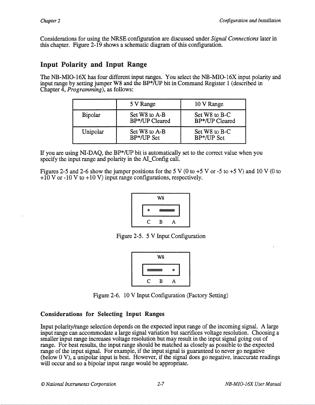
The
input range by setting jumper
Chapter 4,
If
you are using NI-DAQ, the BP*/UP bit is automatically set to the correct value when you
specify the input range and polarity in the AI_ Config call.
Figures 2-5 and 2-6 show the jumper positions for the 5 V
+ 10 V or -10 V to + 10 V) input range configurations, respectively.
Polarity
NB-MI0-16X
Programming), as follows:
Bipolar
Unipolar
and
Input
has four different input ranges. You select the
Range
W8
and the BP*/UP bit
5VRange
SetW8
BP*/UP Cleared BP*/UP Cleared
SetW8
BP*/UP Set BP*/UP Set
to A-B
to A-B
W8
in
Command Register 1 (described in
lOVRange
SetW8
SetW8
(0 to +5 V or -5 to +5 V) and 10 V (0
NB-MI0-16X
toB-C
toB-C
input polarity and
to
I·
--
c B A
Figure 2-5. 5 V Input Configuration
W8
C B A
Figure 2-6. 10 V Input Configuration (Factory Setting)
Considerations
Input polarity/range selection depends on the expected input range
input range can accommodate a large signal variation but sacrifices voltage resolution. Choosing a
smaller input range increases voltage resolution but may result in the input signal going out
range. For best results, the input range should be matched as closely as possible to the expected
of
range
(below O V), a unipolar input
will occur and
the input signal. For example,
for
Selecting
so
a bipolar input range would
Input
is best. However,
Ranges
if
the input signal
if
the signal does go negative, inaccurate readings
be
appropriate.
of
the incoming signal. A large
is
guaranteed to never
go
negative
of
©
National
Instruments
Corporation
2-7
NB-MI0-16X
User
Manual
Page 28
Configuration
and
Installation Chapter2
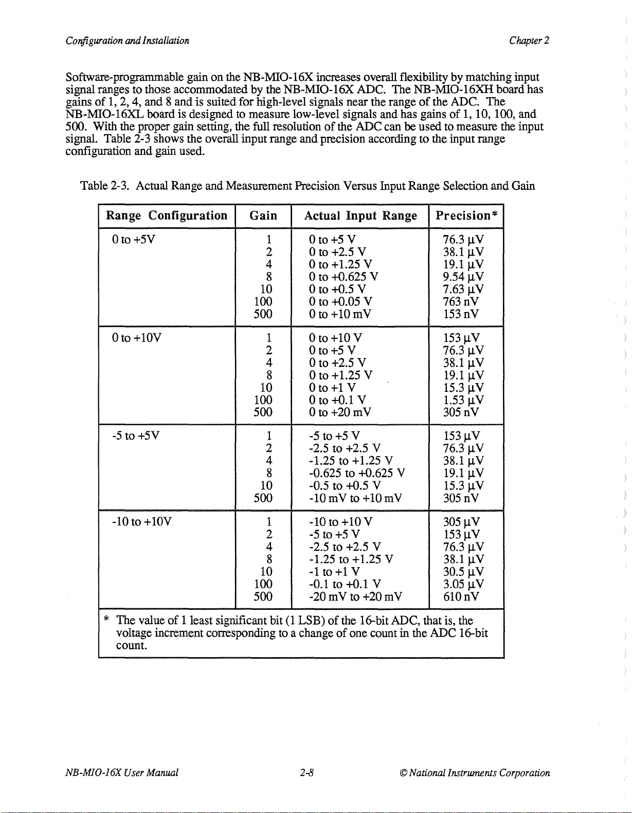
Software-programmable gain on the NB-MI0-16X increases overall flexibility by matching input
signal ranges to those accommodated by the NB-MI0-16X ADC. The NB-MI0-16XH board has
of
1,
gains
2, 4, and 8 and is suited for high-level signals near the range
NB-MI0-16XL board is designed to measure low-level signals and has gains
500. With the proper gain setting, the
signal. Table
2-3 shows the overall input range and precision according to the input range
full resolution
of
the ADC can be used to measure the input
of
the ADC. The
of
l,
10, 100, and
configuration and gain used.
Table 2-3. Actual Range and Measurement Precision Versus Input Range Selection and Gain
Range Configuration Gain Actual Input Range Precision*
Oto+SV 1
2 0
4
8
10
100 0 to +o.05 V
500
Oto+lOV
1
2
4
8 0 to
10
100
500
-5
to +SY
1
2 -2.5 to +2.5 V 76.3
4
8 -0.625 to +o.625 V 19.1
10 -0.5 to +o.5 V 15.3
500
-10 to +lOV
1
2 -5 to
4 -2.5 to +2.5 V 76.3 µV
8 -1.25 to + 1.25 V
10
100 -0.1 to
500 -20 mV to +20
Oto+S
0 to
V
to
+2.5 V 38.1
+l.25
V
76.3
19.1
0 to +o.625 V 9.54
0 to +o.5 V 7.63
763nV
Oto+lOmV
Oto+lOV
0
to+S
V 76.3
153nV
153µV
0 to +2.5 V 38.1
+l.25
Oto+l
Oto+o.l
V
V 15.3
V 1.53
Oto+20mV
-5 to +5 V
19.1 µV
305nV
153µV
-1.25 to + 1.25 V 38.1
-lOmVto+lOmV
-lOto+lOV
+5
V
305nV
305µV
153µV
38.1
-1
to+l
V 30.5
+o.l
V 3.05
mV
610nV
µV
µV
µV
µV
µV
µV
µV
µV
µV
µV
µV
µV
µV
µV
µV
µV
* The value
NB-MI0-16X
of
l least significant bit
(1
LSB)
of
voltage increment corresponding to a change
count.
User
Manual
2-8
the 16-bit ADC, that is, the
of
one count in the ADC 16-bit
© National lnstrwnents
Corporation
Page 29
Chapter
2
Configuration
and
Installation
Analog
You can select different analog output configurations by using the jumper settings shown in
Table 2-1. The following paragraphs describe each
Output
Configuration
of
the analog output configurations in detail.
External and Internal Reference
Each analog output channel can be connected to the NB-MI0-16X internal reference
the external reference signal connected to the EXTREF pin (pin 22) on the
channels need not be configured the same way, although only one
10
V) can be used at a time. (You cannot, for example, use the internal
of
I/0
the internal references
10
V reference on Channel
0 and the internal 5 V reference on Channel 1.)
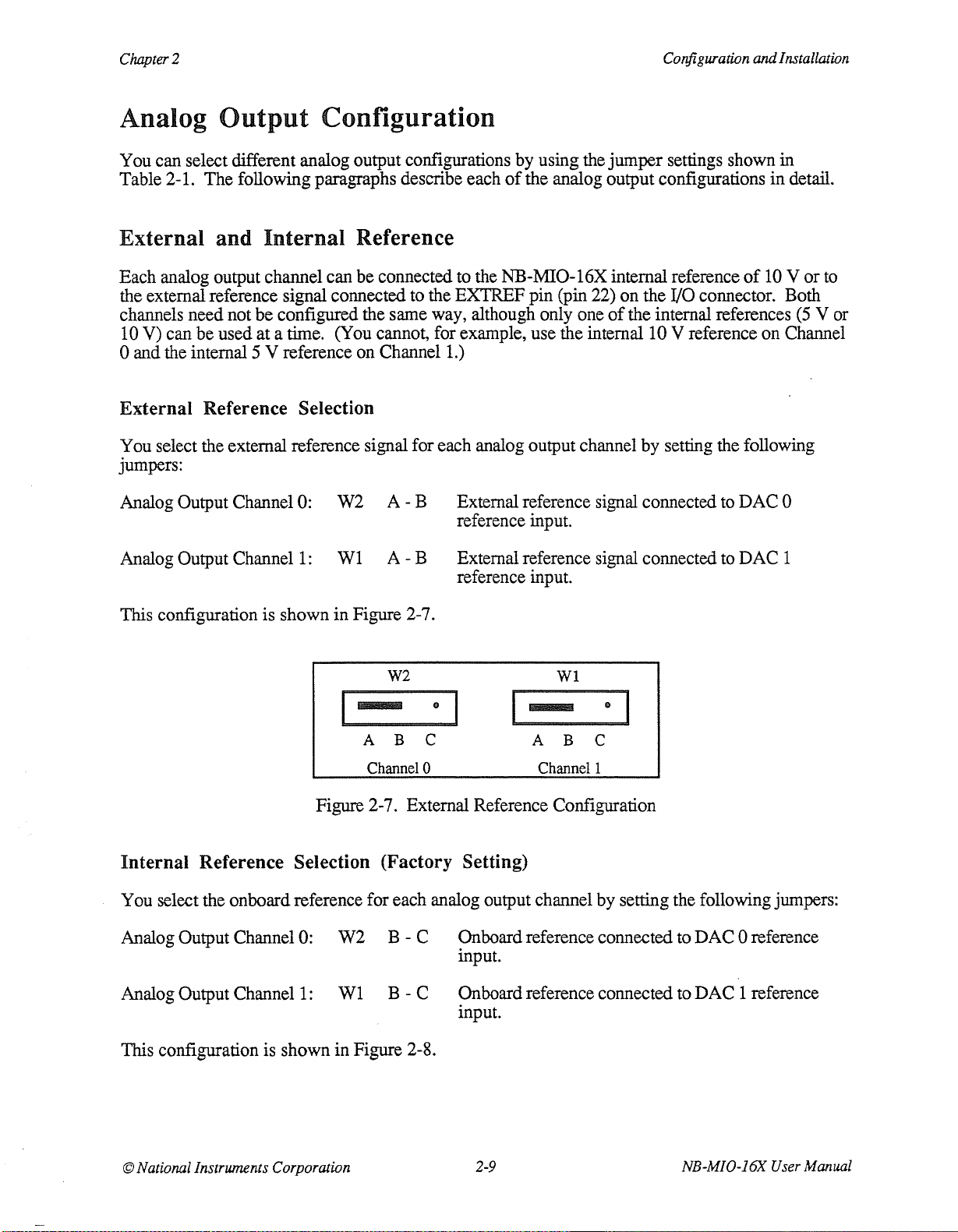
External Reference Selection
You select the external reference signal for each analog output channel by setting the following
jumpers:
Analog Output Channel
Analog Output Channel
0:
W2 A - B External reference signal connected
reference input.
1:
Wl
A - B External reference signal connected to DAC 1
reference input.
of
10 V or
connector. Both
(5
to
DAC 0
to
V or
This configuration is shown
in
Figure 2-7.
W2
- ·I
A B C
Channel 0
Figure 2-7. External Reference Configuration
Wl
- . I
A B C
Channel 1
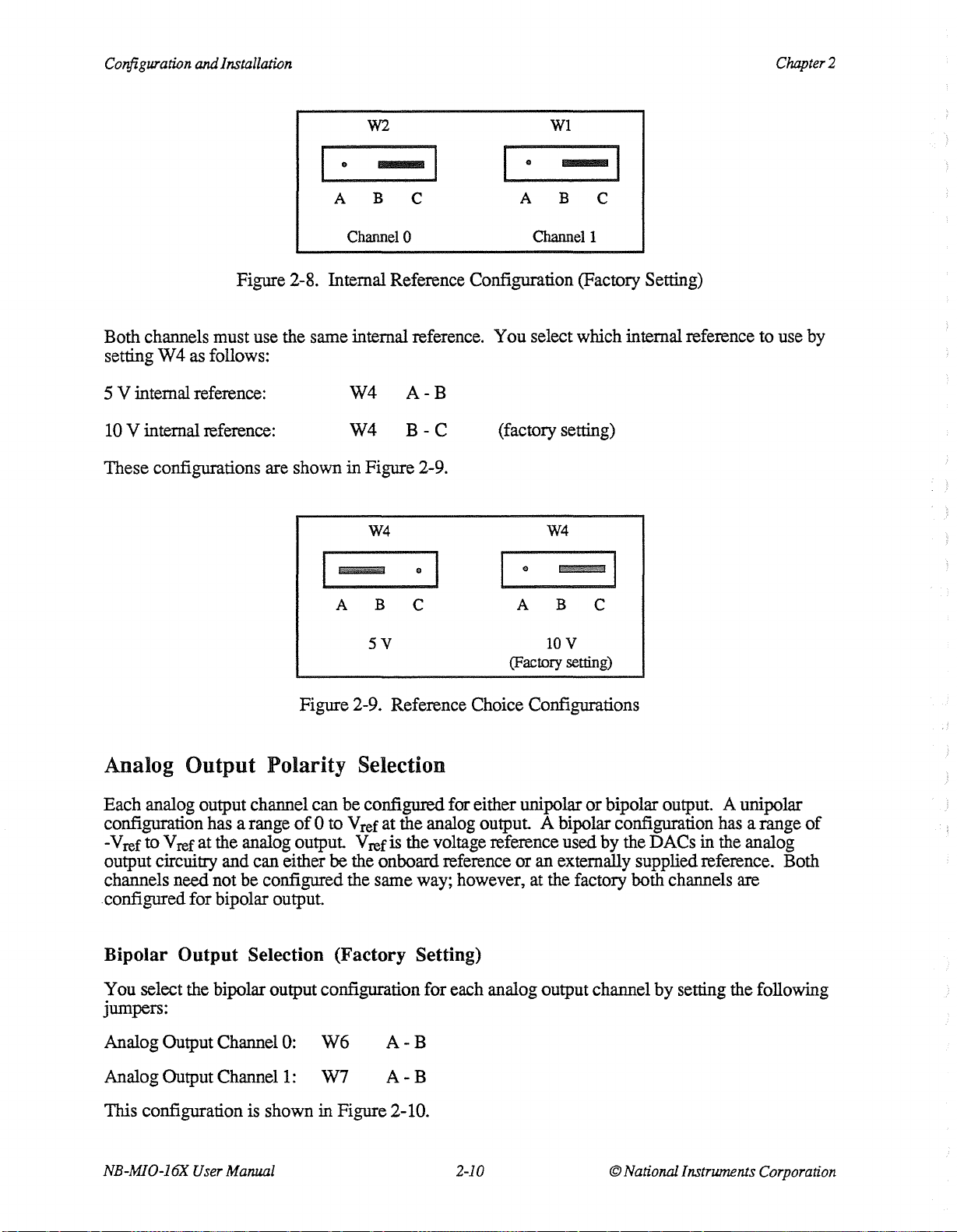
Internal Reference Selection (Factory Setting)
You select the onboard reference for each analog output channel by setting the following jumpers:
0:
Analog Output Channel
Analog Output Channel
This configuration is shown in Figure 2-8.
W2 B - C Onboard reference connected to DAC O reference
input.
1:
Wl
B - C Onboard reference connected to DAC 1 reference
input.
© National Instruments Corporation
2-9
NB-MIO-l
6X
User
Manual
Page 30
Configuration
and.Installation
Chapter2
W2
I·
Figure
Both channels must
setting
5 V internal reference:
10
These configurations are shown in Figure
W4
as
follows:
V internal reference:
use
2-8.
Internal Reference Configuration (Factory Setting)
the
same
-I
A B C A B C
Channel 0 Channel I
internal reference. You select which internal reference
W4
W4
A-B
B-C
W4
2-9.
WI
I·
(factory setting)
-I
W4
to
use
by
A B C
5V
Figure 2-9. Reference Choice Configurations
Analog Output Polarity Selection
Each analog output channel can
configuration
-V ref
to
output circuitry and can either
channels need not
configured for bipolar output.
Bipolar Output Selection (Factory Setting)
You
select
jumpers:
V
has
a range
ref
at
the
analog output V ref
be
the
bipolar output configuration for
of
configured the same
be
configured
Oto Vref at the analog output A bipolar configuration
is
be
the
onboard reference or
for
the voltage reference used
way;
however,
each
I·
(Factory setting)
either unipolar or bipolar output. A unipolar
analog output channel
-I
A B C
IOV
has
by
the
DA
Cs
in
the
an
externally supplied reference. Both
at
the
factory both channels
by
setting
a range of
analog
are
the
following
Analog Output Channel
Analog Output Channel
This configuration
NB-MI0-16X
User
is
shown in Figure 2-10.
Manual
0:
W6 A - B
1:
W7
A - B
2-10
© National Instruments
Corporation
Page 31

Chapter
2
Configuration
and.Installation
111111111111111.
A B C
Figure 2-10. Bipolar Output Configuration (Factory Setting)
When
two's complement
channel range
written
Straight
The data value written
when
you
use the bipolar configuration, you need
to
the DAC. In straight binary mode, data values written
from
O to
4095
decimal
to
the the
Binazy
the following jumpers
analog output channel range
Mode
to
each analog output channel is interpreted
are
set:
Analog Output Straight Binary for
Analog Output Straight Binary for
W6
ChannelO Channel 1
to
select whether
(0
to
OFFF
hex).
from
-2048
Channel
Channel
0:
1:
W7
A B C
In
two's
complement mode, data values
to
2047
W9
WlO
to
write straight binary or
to
the analog output
decimal (F800
as
a straight binary number
to
07FF
A-B
A-B
hex).
This configuration is shown in Figure 2-11.
W9
C
B
A
I
ChannelO
Figure
2-11.
Two's Complement Mode (Factory Setting)
data value written
The
when
the
following jumpers
Analog Output Two's Complement for
to
each analog output channel is interpreted
are
set:
Channel
WlO
..
C
B
I
A
Channel I
Straight Binary Mode
0:
W9
as a two's
B-C
complement number
Analog Output Two's Complement for
This configuration
© National Instruments Corporation
is
shown in Figure 2-12.
Channel
1:
2-11
WlO
B-C
NB-MI0-16X
User
Manual
Page 32

Configuration
and
Installation
Chapter2
W9
C
I
B
A A
ChannelO
Figure 2-12. Two's Complement Mode (Factory Setting)
Unipolar Output Selection
You select the unipolar output configuration for each analog output channel by setting the
following jumpers:
Analog Output Channel 0:
Analog Output Straight Binary for Channel
Analog Output Channel
1:
0:
WlO
C
I
B
Channel 1
W6
W9
W7
B-C
A-B
B-C
W7
-
B
A
Channel 1
WlO
C
B
A
WlO
C
9
I
Analog Output Straight Binary for Channel
Notice that the straight binary format should be used when in unipolar output mode.
This configuration is shown in Figure 2-13.
W6
I .
1:
I .
-
A
B C
Channel 0
W9
9
C
B
A
I
A-B
NB-MI0-16X
User
Manual
Channel 0 Channel 1
Figure 2-13. Unipolar Output Configuration
2-12
© National Instruments
Corporation
Page 33

Chapter
2
Configuration
and
Installation
Note:
If
you are using a software package such as NI-DAQ
reconfigure your software to reflect any changes in
or
Lab
jumper
VIEW
or
2, you may need to
switch settings.
Installation
Within the manual shipped with your Macintosh computer, read the instructions for installing the
unit
video card in the main
Read the entire installation procedure before installing the
can install the
noise performance, you should leave as much room as possible between the
other boards and hardware.
the only other board in the computer, you should install it in Slot 3
NB-MI0-16X
These instructions can be used as a universal board installation guide.
in
For
any
of
the Macintosh NuBus slots. However, to achieve best
instance,
NB-MI0-16X
if
the video board is in Slot 1 and the
into the Macintosh. You
NB-MI0-16X
NB-MI0-16X
or
4.
and
is
Signal Connections
This section describes input and output signal connections to the
NB-MI0-16X
specifications for the signals provided on the
Warning:
I/0
connector. This section includes connection instructions and some
NB-MI0-16X
Connections that exceed any
NB-MI0-16X
computer. Maximum input ratings for each signal are given
discussion
from any such signal connections.
may result in damage to the
of
that signal. National Instruments
of
the maximum ratings
NB-MI0-16X
NB-MI0-16X
I/0
connector.
of
input
board and to the Macintosh
is
not liable for any damages resulting
board via the
or
output signals on the
in
this section under the
The pinout for the
NB-MI0-16X
I/0
connector is shown in Figure 2-14.
©
National
Instruments
Corporation
2-13
NB-MI0-16X
User
Manual
Page 34

Configuration
and
Installation
Chapter2
AIGND
ACHO
ACRI
ACH2
ACH3
ACH4
ACH5
ACH6
ACH7
AI
SENSE
DAClOur
AOGND
ADIOO
ADIOl
ADI02
ADI03
DIGGND
+5
V
EXTS1ROBE*
STOPTRIG
SOURCE!
Ourl
GA1E2
SOURCES
ours
1 2
4
3
5 6
7 8
9
10
12
11
14
13
15 16
17
18
19
20
21
22
23
24
25 26
27
28
29
30
31
32
33 34
35 36
37
38
39
40
41
42
43 44
45
46
47
48
49
50
AIGND
ACH8
ACH9
ACHlO
ACHll
ACH12
ACH13
ACH14
ACH15
DACOOur
EXTREF
DIGGND
BDIOO
BDIOI
BDI02
BDI03
+5
V
SCANCLK
STARTIRIG*
EXTCONV*
GA1El
SOURCE2
0Uf2
GA1E5
Four
Figure 2-14. NB-MI0-16X
I/0
Connector
The signals on the connector can be classified as analog input signals, analog output signals, digital
I/0
signals, digital power connections, and timing
connection guidelines for each
Analog
Pins 1 through 19
Input
Signal Connections
of
the
I/0
of
these groups.
connector are analog input signal pins. Pins 1 and 2 are AI GND
I/0
signals. The following sections have signal
signal pins. AI GND is an analog input common signal that is routed directly to the ground tie
point on the NB-MI0-16X. These pins can be used for a general analog power ground tie point to
the
NB-MI0-16X
connected internally to the negative (-) input of the NB-MI0-16X instrumentation amplifier.
DIFF mode, this signal
if
necessary. Pin 19 is the AI SENSE pin.
is
connected to the reference ground at the output
In
NRSE mode, this pin is
of
the instrumentation
In
amplifier.
NB-MI0-16X
User
Manual
2-14
©
National
Instruments
Corporation
Page 35

Chapter2
Configuration
and
Installation
Pins 3 through
channels
routed
to
signals connected to ACH<7
instrumentation amplifier, and signals connected
input
of
the NB-MI0-16X instrumentation amplifier.
The following input ranges and maximum ratings apply to inputs ACH<15
Differential Input Range
Common Mode Input Range
Input Range
Maximum Input Voltage Rating
Warning:
18
are ACH<15
of
the NB-MI0-16X.
the positive(+) input
..
0>
signal pins. These pins are tied to the 16 analog input
In
single-ended mode, signals connected to
of
the NB-MI0-16X instrumentation amplifier.
..
0> are routed to the positive(+) input
to
ACH<15
..
±lOV
±7 V with respect to NB-MI0-16X AGND
±12 V with respect to
±20 V for
±35 V for
NB-MI0-16X
NB-MI0-16X
Exceeding the differential and common mode input ranges
of
ACH<l5
the
NB-MI0-16X
..
0> are
In
DIFF mode,
8> are routed to the negative(-)
..
0>:
NB-MI0-16X
AGND
board powered off
board powered on
will
result in distorted
input signals. Exceeding the maximum input voltage rating may result in damage
the
NB-MI0-16X
board and to the Macintosh computer. National Instruments is
not liable for any damages resulting from any such signal connections.
of
Connection
analog input signals to the NB-MI0-16X depends on the configuration
NB-MI0-16X analog input circuitry and the type
of
input signal source. The different
of
the
NB-MI0-16X configurations allow the NB-MI0-16X instrumentation amplifier to be used in
of
the
different ways. Figure 2-15 shows a diagram
NB-MI0-16X
instrumentation amplifier.
to
VIN +
o------1
+
V M
Measured
Voltage
Figure 2-15. NB-MI0-16X Instrumentation Amplifier
The NB-MI0-16X instrumentation amplifier applies gain, common-mode voltage rejection, and
high-input impedance to the analog input signals connected to the NB-MI0-16X board. Signals
of
are routed to the positive ( +) and negative (-) inputs
the instrumentation amplifier through input
multiplexers on the NB-MI0-16X. The instrumentation amplifier converts two input signals to a
of
signal that is the difference between the two input signals multiplied by the gain setting
the
© National
Instruments
Corporation
2-15
NB-MI0-16X
User
Manual
Page 36

Configuration
and
Installation
Chapter2
amplifier. The amplifier output voltage is referenced to the
NB-MI0-16X
All signals must
NB-MI0-16X.
at the NB-MI0-16X.
connection at the NB-MI0-16X.
The following sections have connection guidelines for single-ended and differential configurations
and for grounded and floating signal sources.
ADC
measures this output voltage when
be
referenced
If
you have a floating source, you must use a ground-referenced input connection
If
to
ground somewhere, either at the source device or at the
you have a grounded source,
NB-MI0-16X
it
performs
you
must use a non-referenced input
ND
ground. The
conversions.
Types of Signal Sources
When configuring the input mode
first determine whether the signal source is floating or ground-referenced. These two types
signals are described in the following sections.
Floating
A floating signal source is one that is not connected in any way to the building ground system but
rather has an isolated ground reference point. Some examples
outputs
isolation amplifiers. The ground reference
analog input ground in order to establish a local or onboard reference for the signal. Otherwise,
the measured input signal varies or appears to float.
isolated output falls into the floating signal source category.
Signal Sources
of
transformers, thermocouples, battery-powered devices, optical isolator outputs, and
of
the NB-MI0-16X and making signal connections, you must
of
floating signal sources are
of
a floating signal must be tied to the NB-MI0-16X
An
instrument or device that provides an
of
Ground-Referenced
A ground-referenced signal source is one that is connected in some way to the building system
ground and is therefore already connected to a common ground point with respect to the
NB-MI0-16X
isolated outputs
category.
The
difference
system is typically between 1 m V and 100 m V, but can
circuits are not properly connected.
difference may show up as an error in the measurement. The following connection instructions for
grounded signal sources are designed to eliminate this ground potential difference from the
measured signal.
Input
The
NB-MI0-16X
following sections discuss the use
considerations for measuring both floating and ground-referenced signal sources. Table 2-4
summarizes the recommended input configuration for both types
board, assuming that the Macintosh is plugged into the same power system. Non-
of
in
ground potential between two instruments connected
Configurations
Signal
instruments and devices that plug into the building power system fall into this
can
be
configured for one
Sources
to
the same building power
be
much higher
If
a grounded signal source is measured improperly, this
of
three input modes: NRSE, RSE,
of
single-ended and differential measurements, and
if
power distribution
of
signal sources.
or
DIFF. The
NB-MI0-16X
User
Manual
2-16
© National
Instruments
Corporation
Page 37

Chapter
2
Table 2-4. Recommended Input Configurations for Ground-Referenced
and Floating Signal Sources
Configuration
and
Installation
Type
of
Signal
Recommended
Input
Configuration
Ground-Referenced DIFF
(non-isolated outputs,
NRSE
plug-in instruments)
Floating
(batteries, thermocouples,
DIFF with bias resistors
RSE
isolated outputs)
Differential
Connection
Considerations
(DIFF
Configuration)
Differential connections are those in which each NB-MI0-16X analog input signals has its own
reference signal or signal return path. These connections are available when the
configured in the DIFF mode. Each input signal is tied to the positive(+) input
instrumentation amplifier, and its reference signal, or return, is tied to the negative (-) input
NB-MI0-16X
of
the
of
the
instrumentation amplifier.
When the NB-MI0-16X is configured for DIFF input, each signal uses two
of
the multiplexer
inputs-one for the signal and one for its reference signal. Therefore, only eight analog input
The
channels are available when using the DIFF configuration.
be
used when any
of
the following conditions are present:
DIFF input configuration should
is
• Input signals are low-level (less than 1 V).
• Leads connecting the signals
• Any
of
the input signals requires a separate ground reference point or return signal.
to
the NB-MI0-16X are greater than 15
ft
• The signal leads travel through noisy environments.
Differential signal connections reduce induced noise and increase common mode signal and noise
rejection. They also permit input signals to float within the common mode limits
of
the input
instrumentation amplifier.
Differential Connections for
Figure 2-16 shows how to connect a ground-referenced signal source to an
configured for DIFF input. Configuration instructions are included under
Configuration
earlier in this chapter.
Grounded
Signal
Sources
NB-MI0-16X
Analog Input
board
© National Instrwnents
Corporation
2-17
NB-MI0-16X
User
Manual
Page 38

Configuration and Installation
Chapter2
Ground-
Referenced
Signal
Source
Common
Mode
Noise,
Ground
etc.
3
5
7
ACH<0
..
..
4
6
8
ACH<8
..
..
Input Multiplexers
AI
SENSE
..
7>
..
15>
AIGND
+
Measured
Voltage
I/0
Connector
NB-MI0-16X Board
in DIFF Configuration
Figure 2-16. Differential Input Connections for Grounded Signal Sources
type
of
With this
connection, the instrumentation amplifier rejects both the common mode noise in
the signal and the ground potential difference between the signal source and the NB-MI0-16X
cm
in
ground (shown as V
Figure 2-16).
Differential Connections for Floating Signal Sources
Figure 2-17 shows how to connect a floating signal source
for DIFF
input
Configuration instructions are described under Analog Input Configuration earlier
in this chapter.
to
an
NB-MI0-16X
board configured
NB-MI0-16X
User
Manual 2-18
© National Instruments
Corporation
Page 39

Chapter2
Configuration
and Installation
Floating
Signal
Source
Bias
Current
Return
Paths
1 1
(
3
5
7
4
6
8
19
<>+----1
ACH<0
•
•
ACH<8
..
Input Multiplexers
AI
SENSE
..
..
7>
15>
+
Measured
Voltage
I/0
Connector
in
DIFF
NB-MI0-16X Board
Configuration
Figure 2-17. Differential Input Connections for Floating Sources
The
100
kQ
resistors shown in Figure 2-17 create a return path to ground for the bias currents
the instrumentation amplifier.
If
a return path is not provided, the instrumentation amplifier bias
of
currents charge up stray capacitances, resulting in uncontrollable drift and possible saturation in the
amplifier. Typically, values from 10
to 100
kQ
are used.
kQ
A resistor from each input to ground, as shown in Figure 2-17, provides bias current return paths
for an AC-coupled input signal. This solution, although necessary for AC-coupled signals, lowers
of
the input impedance
the analog input channel. In addition, the input offset current
instrumentation amplifier contributes a
of
±15
maximum input offset current
by
the 100
offset voltage drift
kQ
resistor,
of
this
current contributes a maximum offset voltage
2 µV/°C at the input. Keep this in mind when you observe DC offsets with
nA
DC
offset voltage at the
input
and a typical offset current drift
The
amplifier has a
of
±20
of
1.5 mV and a typical
of
pN°C.
the
Multiplied
AC-coupled inputs.
If
the input signal is DC-coupled, then only the resistor connecting the negative (-) signal input to
ground is needed.
or
cause an offset at the
This connection does not lower the input impedance
input
of
the analog input channel
© National Instruments
Corporation
2-19 NB-MI0-16X
User
Manual
Page 40

Configuration
and
Installation
Chapter2
Single-Ended Connection Considerations
Single-ended connections are those in which all NB-MI0-16X analog input signals are referenced
to
one common ground. The input signals are tied to the positive ( +) input
of
the instrumentation
amplifier, and their common ground point is tied to its negative (-) input.
When the
NB-MI0-16X
is configured for single-ended input (NRSE or RSE), 16 analog input
channels are available. Single-ended input connections can be used when the following criteria are
met by all input signals:
..
Input signals are high-level (greater than 1 V).
..
Leads connecting the signals
..
All input signals share a common reference signal (at the source).
If
any
of
the above criteria is not met, using DIFF input configuration is recommended.
The NB-MI0-16X can be jumper configured for two different types
RSE configuration and NRSE configuration. The RSE configuration
to
the NB-MI0-16X are less than 15 ft.
of
single-ended connections-
is
used for floating signal
sources. In this case, the NB-MI0-16X provides the reference ground point for the external
signal. The NRSE configuration is used for ground-referenced signal sources. In this case, the
external signal supplies its own reference ground point and the NB-MI0-16X should not supply
one.
Single-Ended Connections for Floating Signal Sources (RSE Configuration)
Figure 2-18 shows how to connect a floating signal source
for single-ended
input
input to make these types
Input Configuration
The NB-MI0-16X analog input circuitry must be configured for RSE
of
connections. Configuration instructions are included under Analog
earlier in this chapter.
to
an NB-MI0-16X board configured
Floating
Signal
Source
NB-MI0-16X
ACH<0
..
15>
..
1,2
I/0
Connector
Figure 2-18. Single-Ended Input Connections for Floating Signal Sources
User
Manual
Input Multiplexer
NB-MI0-16X Board
2-20
in
RSE
Configuration
©
National
Measured
Voltage
Instruments
Corporation
Page 41

Chapter2
Configuration
and
Installation
Single-Ended Connections for Grounded Signal Sources (NRSE Configuration)
If
a grounded signal source is to
NB-MI0-16X
positive (
reference
ground point
difference between the
must be configured
+) input
is
of
the
NB-MI0-16X
connected to the negative(-) input
of
the signal should therefore be connected to the AI SENSE pin.
NB-MI0-16X
signal at both the positive ( +) and negative (-) inputs
difference
NB-MI0-16X
potentials appears as
is rejected
by
the amplifier. On the other hand,
is referenced to ground, such as
an
error
be
measured with a single-ended configuration, then the
in
the NRSE input configuration.
The
signal
instrumentation amplifier and the signal local ground
of
the
NB-MI0-16X
instrumentation amplifier. The
ground and the signal ground appears as a common mode
of
the instrumentation amplifier, and this
if
the input circuitry
in
the RSE configuration, this difference in ground
in
the measured voltage.
is
connected to the
Any
potential
of
the
Figure 2-19 shows how to connect a grounded signal source to an
in
the NRSE configuration. Configuration instructions are included under Analog Input
Configuration
Grmmd-
earlier
in
this chapter.
•
ACH<0
..
15>
NB-MI0-16X
board configured
•
Input Multiplexer
+
Measured
Voltage
I/0
Connector
NB-MI0-16X Board
Figure 2-19. Single-Ended Input Connections
in NRSE Input Configuration
for
Grounded Signal Sources
Common Mode Signal Rejection Considerations
Figures 2-16 and 2-19 show connections for signal sources that are already referenced to some
ground point with respect to the
reject any voltage due to ground potential differences between the signal source and the
NB-MI0-16X.
In addition, with differential input connections, the instrumentation amplifier can
reject common mode noise pickup
©
National
Instruments Corporation
NB-MI0-16X.
in
the leads connecting the signal sources to the NB-MI0-16X.
In these cases, the instrumentation amplifier can
2-21
NB-MI0-16X
User
Manual
Page 42

Configuration
The
common
magnitude
The
common
signal
formula for the allowed
V
cm-max
and Installation
of
01
diff =
mode
input range
the greatest
mode
input range for the
v+in -v-in)
= ± (12V - 2 )
of
the
NB-MI0-16X
common
and the gain setting
common
cliff * Gain
V
mode signal that
mode
can
NB-MI0-16X
of
the instrumentation amplifier.
input
range is
instrumentation amplifier is defined
be
rejected.
depends on the size
as
follows:
of
the differential input
The
exact
Chapter2
as
the
where
For
mode
of
The
calculated
where
signal
If
you need to limit the amount
NB-MI0-16X
the maximum value for V
±lOVrange
0 to +10 V range
±5
Vrange
example, for a differential voltage as large as
voltage that can
500, ±9.5 V
common
V
cm-actual = 2
V\n
at
the negative (-) input
the input signal
common
mode
by
the following formula:
is
the signal
ground.
be
rejected is ±7 V. However,
mode
voltage is measured with respect
cv+in + v-in)
at
common
cliff
is as follows:
V cliff-max =
V cliff-max = 10 V
cliff-max = ±5 V
V
voltage
the positive ( +) input
of
mode
of
floating that occurs
can
the instrumentation amplifier.
range exceeds ±7 V
±10
be
V
20
m V
and
a gain
if
the
differential signal is 10 m V with a gain
rejected.
to
the
NB-MI0-16X
of
the instrumentation amplifier and
with
respect to the
between
the signal ground and the
of
500, the largest
ground and
NB-MI0-16X
can
v-in
common
be
is the
ground,
Analog
Pins 20 through 23
Pins
output signal
output
Pin
22,
output channel
signal applied
configuration instructions are described under
The
following ranges and ratings apply to the
Useful input voltage range:
Absolute maximum ratings:
NB-MIO-I6X
Output
of
20
and 21 are the DACO
for
analog output channel 0.
channel 1.
EXTREF,
User
is the external reference input for
must
be
at
the external reference input to be used
Manual
Signal Connections
the
I/0
connector
OUT
configured individually for external reference selection
and
are
analog
DACl
DACl
output
OUT
OUT
signal pins.
signals pins. DACO
OUT
is the voltage
is the voltage output signal for analog
both
analog output channels.
by
that channel. Analog output
in
Each
order
analog
for
the
Analog Output Configuration earlier in this chapter.
EXTREF
±10 V peak
±25 V
2-22
input:
with respect to
peak
with respect to
AO
GND
AO
GND
© National Instruments
Corporation
Page 43

Chapter2
Configuration
and
Installation
Pin 23,
AO
GND, is the ground reference point for both analog output channels and for the
external reference signal.
Figure 2-20 shows how to make analog output connections and the external reference input
connection to the
NB-MIQ..16X board.
If
neither channel is configured to use an external
reference signal, do not connect anything to the EXTREF pin.
EX1REF
22
DACOOUT
External
Reference
Signal
(Optional)
Load
Load
VOUTO
VOUTl
+
+
20
DAClOUT
21
Channel 0
Channel 1
Analog Output Channels
NB-MI0-16X Board
Figure 2-20. Analog Output Connections
The external reference signal can be either a DC or an AC signal. This reference signal is
multiplied by the DAC code to generate the output voltage.
Digital
Pins 24 through 32
Pins 25, 27, 29, and
26, 28, 30, and 32 are connected to the digital lines
DIG GND, is the digital ground pin for both digital
I/0
Signal Connections
of
the
I/0
connector are digital
31
are connected to the digital lines
I/0
signal pins.
ADI0<3:0>
BDI0<3:0>
I/0
ports. Ports A and B can be programmed
for digital
for digital
I/0
port A Pins
I/0
port B. Pin 24,
individually to be inputs or outputs.
The following specifications and ratings apply to the digital
I/0
lines:
Absolute maximum voltage
input rating:
5.5 V with respect to DIG GND
© National Instruments Corporation
2-23
NB-MI0-16X
User
Manual
Page 44

Configuration
and
Installation
Digital Input Specifications (referenced to DIG GND):
Chapter2
Vrn input logic high voltage:
Vn...
input logic low voltage:
Irn
input current load,
logic high input voltage:
Irr..
input current load,
logic low input voltage:
2Vminimum
0.8 V maximum
µA maximum
40
µA maximum
-120
Digital Output Specifications (referenced to DIG GND):
OH
output logic high voltage:
V
VOL
output logic low voltage:
2.4 V minimum
0.5 V maximum
IoH output source current,
mA
mA
maximum
maximum
11
logic high:
loH
output sink current,
logic low:
2.6
24
With these specifications, each digital output line can drive
TTL
loads.
Figure 2-21 depicts signal connections for three typical digital
standard
I/0
applications.
TTL
loads and over 50 LS
NB-MI0-16X
User
Manual
2-24
©
National
Instruments
Corporation
Page 45

Chapter2
LED
+5 V
31
29
27
25
32
Configuration
Port A
ADI0<3
.. 0>
and
Installation
TTL Signal
30
28
+5V
Switch
I/0
Connector
Figure 2-21. Digital
In Figure
2-21, port A is configured for digital output, and port
Digital input applications include receiving
the state
of
the switch
in
Figure 2-21. Digital output applications include sending
TIL
26
24
DIGGND
I/0
Connections
signals and sensing external device states such
driving external devices such as the LED shown in Figure
2-21.
PortB
BDICk3
NB-:rvIT0-16X
Bis
configured for digital input.
..
0>
Board
TIL
as
signals and
Power Connections
Pins 34 and 35
are referenced to DIG GND and can
Power rating:
Warning:
©
National
of
the
I/0
connector provide
0.5Aat+5V±10%
Under no circumstances should these +5 V power pins be connected directly
or
digital ground or to any other voltage source on the NB-MI0-16X or any other
device. Doing so may damage the
Instruments
Instruments
is not liable for damage resulting from such a connection.
Corporation
be used
+5
V from the Macintosh power supply. These pins
to
power external digital circuitry.
to
NB-MI0-16X and the Macintosh. National
2-25
NB-MJ0-16X
User
analog
Manual
Page 46

Configuration
and
Installation
Timing Connections
Chapter2
Pins 36 through 50
40 carry signals used for
Acquisition Timing Connections later in this chapter. Pins 41 through 50 carry general-purpose
of
the
I/0
connector are connections for timing
data acquisition timing. These signals are explained under
I/0
signals. Pins 36 through
Data
timing signals provided by the onboard Am9513A Counter!fimer. These signals are explained
under
Data
General-Purpose Timing Signal Connections later
Acquisition Timing Connections
in
this chapter.
The data acquisition timing signals are SCANCLK, EXTSTROBE*, STARTTRIG*, STOPTRIG,
and EXTCONV*.
SCANCLK is an output signal that generates a low-to-high edge whenever an
ND
conversion
begins. SCANCLK pulses only when scanning is enabled on the NB-MI0-16X. SCANCLK is
normally high and pulses low for approximately 1
µsec
before the
ND
conversion begins. The
low-to-high edge can be used to clock external analog input multiplexers. The SCANCLK signal
is driven
by
one LS
TTL
gate.
A low pulse is generated on the EXTSTROBE* pin when the External Strobe Register is loaded
(see
External Strobe Register in Chapter 4, Programming). Figure 2-22 shows the timing for the
EXTSTROBE* signal.
65
nsec
minimum
90
nsec
typical
Figure 2-22. EXTSTROBE* Signal Timing
The pulse is typically 90 nsec and is a minimum 65 nsec
LS TTL signal that can be used
ND
conversions can be externally triggered with the EXTCONV* pin. Applying an active low
pulse
to
the EXTCONV* initiates an
to-high edge
of
the applied pulse. Figure 2-23 shows the timing requirements for the EXTCONV*
by
an external device to latch signals
ND
conversion.
in
width. The EXTSTROBE* signal is an
or
trigger events.
The
ND
conversion is initiated by the low-
signal.
NB-MI0-16X
User
Manual
2-26
©
National
Instruments
Corporation
Page 47

Chapter
The minimum allowed pulse width is
low-to-high edge. There is no maximum pulse width limitation. EXTCONV* should be high for
at least 50 nsec before going low. The EXTCONV* signal is one LS
+5 V through a 4.7
2
ill
ND
conversion starts within
100 nsec from this point
Figure 2-23. EXTCONV* Signal Timing
50
nsec.
An
AID conversion starts within 100 nsec
resistor.
Configuration
lw 50 nsec minimum
TTL
load and is pulled up to
and
Installation
of
the
Note:
Any data acquisition sequence controlled
be initiated by an external trigger applied to the STARTTRIG* pin.
by the EXTCONV* signal,
counters are initialized and armed, applying a falling edge to the
counters, thereby initiating a data acquisition sequence.
The data acquisition operation is initiated by the high-to-low edge
2-25 shows the timing requirements for the STARTTRIG* signal.
EXTCONV* is also driven by the output
This counter is also referred to as the sample-interval counter. The output
must be disabled to a high-impedance state
pulses applied to the EXTCONV* pin.
output signal can be monitored at the EXTCONV* pin.
by
STARTIRIG*
vlli-~-0;;:.~
V
1L
-=--tw-=--~i
[ tw 50 nsec minimum
of
Counter 3
if
AID conversions are to be controlled
If
Counter 3 is used to control AID conversions, its
the onboard sample-interval and sample counters can
does not affect the acquisition timing. Once the two
~
of
the Am9513A Counterffimer.
STARTIRIG*
}----
of
Counter 3
If
conversions are generated
pin starts the
of
the applied pulse. Figure
by
First
ND
conversion starts within
1 sample interval from this point
Figure 2-24. STARTTRIG* Signal Timing
The
first
AID
The minimum allowed pulse width is 50 nsec.
interval from the high-to-low edge. The sample interval is controlled
of
period is the clock period
© National
Instruments
Corporation
the timebase or source signal used
2-27
conversion starts within one sample
by
the sample-interval counter.
by
Counter 3. This clock
NB-MIO-l6X
User
Manual
Page 48

Configuration
and
Installation
Chapter2
There is no maximum pulse width limitation; however,
50
nsec before going low. The STARTIRIG* signal is one LS TTL load and is pulled up to +5 V
kO
through a 4.7
The STOPTRIG pin
resistor.
is used during NB-MI0-16X pretriggered data acquisition operations. In
STARTIRIG*
should be high for at least
pretriggered mode, the data acquisition operation is started but no sample counting occurs until a
rising edge is applied to the STOPTRIG pin. The acquisition then completes when the sample
counter decrements
to
0. This mode acquires data both before and after a hardware trigger is
received. Figure 2-25 shows the timing requirements for the STOPTRIG signal.
Figure 2-25. STOPTRIG Signal Timing
The STOPTRIG signal is pulled up to +5 V through a 4.7
kQ
resistor.
General-Purpose
Timing
Signal Connections
The general-purpose timing signals include the GATE, SOURCE, and OUT signals for the
Arn9513A Counters
and 5
of
the Arn9513A Counterffimer can be used for general-purpose applications such as pulse
1,
2, and 5, and the FOUT signal generated
by
the Arn9513A. Counters
1,
2,
and square wave generation, event counting, and pulse-width, time-lapse, and frequency
measurements. For these applications, SOURCE and GATE signals can be directly applied to the
counters from the
The Arn9513A Counterffimer
programming information, consult the Arn9513A data sheet
I/0
connector, and the counters are programmed for various operations.
is described briefly in Chapter 3, Theory
in
Appendix C,
of
Operation. For detailed
AMD
Data Sheet. For
detailed applications information, consult the technical manual The Am9513A/Am9513 System
Timing Controller published by Advanced Micro Devices, Inc.
Pulses and square waves can be produced by programming Counter 1, 2, or 5 to generate a pulse
signal at its OUT output pin or to toggle the OUT signal each time the counter reaches the terminal
count.
For event counting, one
any
of
the Arn9513A SOURCE inputs. The counter value can then be read to determine the
of
the counters is programmed to count rising or falling edges applied to
number of edges that have occurred. Counter operation can be gated on and off during event
counting. Figure 2-26 shows connections for a typical event-counting operation where a switch is
used to gate the counter on and off.
NB-MI0-16X
User
Manual
2-28
©
National
Instruments
Corporation
Page 49

Chapter
2
Con.figuration
and
Installation
our
GATE
Switch
Signal
Source
IJO
33
Connector
NB-:MI0-16X Board
Counter
Figure 2-26. Event-Counting Application with External Switch Gating
To
perform pulse-width measurement, a counter is programmed to be level gated. The pulse to
measured is applied
signal at the GATE input is either high
timebase, then the pulse width is equal
For
time-lapse measurement, a counter
counter GATE input to start the counter. The counter can
receiving either a high-to-low edge or a low-to-high edge.
an internal timebase, then the time lapse since receiving the edge
to
the counter GATE input.
or
to
is
The
low.
counter
If
the counter is programmed
is
programmed to count while the
to
count an internal
the counter value multiplied by the timebase period.
programmed to be edge gated. An edge is applied to the
be
programmed to start counting after
If
the counter is programmed
is equal to the counter value
multiplied by the timebase period.
to
be
count
To
measure frequency, a counter is programmed to
counted in a signal applied to a SOURCE input.
of
some known duration. In this case, the counter is programmed to count either rising
is
falling edges at the SOURCE input while the gate is applied.
be
level gated and the rising
The
gate signal applied to the counter GATE input
The
frequency
or
falling edges are
of
the input signal
or
then the count value divided by the known gate period. Figure 2-27 shows the connections for a
be
frequency measurement application. A second counter could also
used to generate the gate
signal in this application.
© National Instruments
Corporation
2-29
NB-MI0-16X
User
Manual
is
Page 50

Configuration
and
Installation
Chapter2
our
GATE
Signal
Source
I/0
Gate
Connector
33
DIGGND
Figure 2-27. Frequency Measurement Application
Two
or
more counters can be concatenated by tying the OUT signal from one counter
of
SOURCE signal
another counter. The counters can then be treated as one 32-bit or 48-bit
counter for most counting applications.
1,
The GATE, SOURCE, and OUT signals for Counters
2, and 5, and the FOUT output signal are
tied directly from the Am9513A input and output pins to the
and SOURCE pins are pulled up to +5 V through a 4.7
ill
NB-MI0-16X
I/0
connector.
resistor.
Counter
Board
In
to
the
addition, the
GA
TE
The following specifications and ratings apply
to
the Am9513A
I/0
Absolute maximum voltage
input rating:
V to + 7 .0 V with respect to
-0.5
Am9513A Digital Input Specifications (referenced to DIG GND):
Vrn:
input logic high voltage: 2.2 V minimum
VIL input logic low voltage: 0.8 V maximum
Input load current:
±10
µA
maximum
Am9513A Digital Output Specifications (referenced to DIG GND):
OH
output logic high voltage: 2.4 V minimum
V
NB-MI0-16X
User
Manual
2-30
signals:
© National
DIG
GND
Instruments
Corporation
Page 51

Chapter2
Configuration and
Installation
VOL
output logic low voltage:
loH
output source current,
atVoH:
output sink current,
IoH
atVoL:
0.4 V maximum
200
3.2
Output current, high-impedance
state:
±25
Figure 2-28 shows the timing requirements for the
timing specifications for the
SOURCE
GATE
V
V
IB
n.,
OUT
output signals
of
µA
maximum
mA
maximum
µA
maximum
GATE
and SOURCE input signals and the
the Am9513A.
lgw
lout
our
145 nsec minimum
lsc
tsp
lgsu
lgh
lgw
tout
Figure 2-28. General-Purpose Timing Signals
The
GATE
SOURCE
edges.
of
the source signal, applies to the case in which the counter is programmed to count falling edges.
and
OUT
signal transitions
signal. This timing diagram assumes that the counters are programmed to count rising
The
same timing diagram, with the source signal inverted and referenced to the falling edge
The signal applied at a SOURCE input can
counter/timers and
by
the Am9513A frequency division output FOUT.
SOURCE input must not exceed a frequency
be
Am9513A counters can
applied
at
any
of
the Am9513A SOURCE
individually programmed to count rising or falling edges
70 nsec minimum
100 nsec minimum
10 nsec minimum
145
nsec
minimum
300
nsec
maximum
in
Figure 2-28 are referenced to the rising edge
be
used as a clock source by any
of 6 MHz
or
GATE
for proper operation
input pins.
of
the Am9513A
The
signal applied to a
of
the Am9513A. The
of
of
signals
the
© National Instruments Corporation
2-31
NB-MI0-16X
User
Manual
Page 52

Configuration
and Installation
Chapter2
In addition to the signals applied to the SOURCE and
internal timebase clocks from the clock signal supplied by the NB-MI0-16X. These clocks can be
used as counting sources, and they have a maximum skew
in
SOURCE signal shown
GA
TE
inputs,
AMD
Data Sheet, for further details.
Specifications for signals at the GATE input are referenced to the signal at the SOURCE input or
of
one
to the rising edge
before the rising or falling edge
shown by
after the rismg
gate high or low period must be at least 145 nsec in duration.
the gate signal cannot be synchronized with the clock.
edge take effect either on that source edge or on the next one.
uncertainty
Signals generated at the OUT output are referenced to the signal at the SOURCE input
the Am9513A internally generated clock signals. Figure 2-28 shows the
the rising edge
source signal rising
the Am9513A internally generated signals. Figure 2-28 shows the
Cabling
inputs,
of
a source signal. The gate must be valid (either high
tgsu
and
!izh
or
falling edge
of
one source clock period with respect to unsynchronized gating sources.
of
a source signal. Any OUT signal state changes occur within 300 nsec after the
or
and
Figure 2-28 represents any
or
internal timebase clocks. See the Am9513A data sheet in Appendix C,
of
a source signal for the gate to take effect at that source edge (as
in Figure 2-28). Similarly, the gate signal must
of
a source signal for the gate to take effect at that source edge. The
falling edge.
Field
Wiring
GATE
of
inputs, the Am9513A generates five
of
7 5 nsec between them. The
the signals applied at the SOURCE
GATE
or
be
held for at least 10 nsec
If
an internal timebase clock is used,
In
this case, gates applied close to a source
signal referenced
low) at least 100 nsec
This arrangement provides an
or
OUT
signal referenced to
to one
of
This section discusses cabling and field wiring guidelines for the
Field
Accuracy
environmental noise
between signal sources and the NB-MI0-16X board. The following recommendations apply
mainly to analog input signal -routing to the
signal routing in general.
Noise pickup can be minimized and measurement accuracy maximized by doing the following:
• Use individually shielded, twisted-pair wires
• Use differential analog input connections to reject common mode noise.
The following recommendations apply for all signal connections to the NB-MI0-16X:
• Physically separate
Wiring
of
measurements made with the NB-MI0-16X can
NB-MI0-16X. With this type
twisted together and then covered with a shield. This shield is then connected at only one point
to the signal source ground. This kind
areas with large magnetic fields or high electromagnetic interference.
lines are capable
run in parallel paths at a close distance. Reduce the magnetic coupling between lines
separating them
angles to each other.
Considerations
if
proper considerations are not taken into account when running signal wires
NB-MI0-16X
to
connect analog input signals to the
of
wire, the signals attached to the
of
connection is required for signals traveling through
NB-MI0-16X
of
inducing currents in or voltages on the
by
a reasonable distance
signal lines from high-current
if
they run in parallel, or by running the lines at right
board, though they are applicable for
NB-MI0-16X
be
seriously affected by
CH+
and CH- inputs are
or
high-voltage lines. These
NB-MI0-16X
signal lines
board.
if
by
they
NB-MI0-16X
User
Manual
2-32
© National
Instruments
Corporation
Page 53

Chapter
2
Configuration
and
Installation
• Do not run
• Protect
equipment, breakers, or transformers by running the
NB-MI0-16X
NB-MI0-16X
signal lines through conduits that also contain power lines.
signal lines from magnetic fields caused by electric motors, welding
NB-MI0-16X
signal lines through special
metal conduits.
Cabling
Considerations
National Instruments has a cable termination accessory, the CB-50, for use with the NB-MI0-16X
board. This kit includes a terminated 50-conductor flat ribbon cable and a connector block. Signal
I/0
leads can
NB-MI0-16X
be
attached
I/0
to
screw terminals on the connector block and thereby connected to the
connector.
The CB-50 is useful for prototyping an application or in situations where NB-MI0-16X
interconnections are frequently changed. Once a final field wiring scheme has been developed,
to
however, you may wish
guidelines for design
The NB-MI0-16X
I/0
develop your own cable. This section contains information and
of
such a cable.
connector is a 50-pin male ribbon cable header. Recommended
manufacturer part numbers for this header are as follows:
3M Scotchflex
T &B Corporation/ Ansley Electronics Division
part number 3596-5002
part number 609-5007
The mating connector for the NB-MI0-16X is a 50-position, ribbon socket connector, polarized,
with strain relief. National Instruments uses a polarized (keyed) connector to prevent inadvertent
upside down connection to the NB-MI0-16X. Recommended manufacturer part numbers for this
mating connector are as follows:
3M
Scotchflex
T &B Corporation/ Ansley Electronics Division
part number 3425-7650
part number 609-5041CE
A standard ribbon cable (50-conductor, 28 A WG, stranded) can be used with these connectors.
Recommended manufacturer part numbers for this ribbon cable are as follows:
3M Scotchflex
T &B Corporation/ Ansley Electronics Division
In making your own cabling, you may want
to
shield your cables. The following guidelines may
part number 3365/50
part number 171-50
help:
For the analog input signals, shielded twisted-pair wires for each analog input pair yield the
best results, assuming that differential inputs are used. Tie the shield for each signal pair to the
at
ground reference
the source.
The analog lines, pins 1 through 23, should be routed separately from the digital lines, pins 24
through 50.
of
When using a cable shield, use separate shields for the analog and digital halves
the cable.
Failure to do so will result in noise from switching digital signals coupling into the analog
signals.
©
National
Instruments
Corporation
2-33
NB-MI0-16X
User
Manual
Page 54

Chapter
3
Theory
This chapter contains a functional overview
each functional unit making up the NB-MI0-16X.
of
Operation
of
the NB-MI0-16X and explains the operation
Functional Overview
The block diagram
in
Figure 3-1 is a functional overview
RTSIBus
RI'SI
Bus
of
Interface
of
the NB-MI0-16X board.
<I)
=
=
=
z
Internal
Data
C)
u
~
£
C:
<n
-
~
Internal
i Control
Data
Acquisition
Bus
Bus
Figure 3-1. NB-MI0-16X Block Diagram
Tlffiing
Analog
Output
Digital
I/0
©National
Instrumerus
Corporation
3-1
NB-MI0-16X
User
Manual
Page 55

Theory
of
Operation
Chapter3
The following are the major constituents
• NuBus interface circuitry
0
Analog input and data acquisition circuitry
• Analog output circuitry
• Digital
• Timing
• RTSI bus interface circuitry
The internal data and control buses interconnect the components. The theory
of
these components is explained in the remainder
I/0
1/0
circuitry
circuitry
of
the
NB-MI0-16X
of
this chapter.
board:
NuBus Interface Circuitry
The
NB-MI0-16X
data bus with a 10
write operations, and an interrupt line that may be driven by boards
components making up the
is a full-sized 16-bit NuBus slave board. The NuBus is a 32-bit address and
MHz
clock.
In
addition, the NuBus provides interface signals for read and
NB-MI0-16X
in
NuBus slots. The
NuBus interface circuitry are shown
of
operation
in
Figure 3-2.
of
each
/CLOCK (10
NuBus
"'
=
_ /AD<31:0>
=
=
z
- NMR
-
/ID
<3:0>
Trrninl?
:MHz)
32
\
.
-
I
Hli""
l..jll!lo,
-
-
-
l
NuBus
Interface
Tuning
Data
Transceivers
Address
Latches
Slot
Decoder
On
board
Clock
Generation
1~
-
l..jll!lo,
r-1111='
i..a,..
.
'
Configuration
ROM
•
Address
Decoder
•
-
10
:MHz
:MHz
1
Read and Write
Signals
Internal
Data Bus
Internal
Address
Bus
Register
Selects
NB-1v1I0-16X
Interrupt
Clock
Clock
NB-MI0-16X
Figure 3-2. NuBus Interface Circuitry Block Diagram
User
Manual
3-2
© National Instruments Corporation
Page 56

Chapte:r
The NuBus interface circuitry consists of slot-decoding circuitry, address latches, data
transceivers, interface timing signals, address decoding circuitry, EPROM,
circuitry, and circuitry to generate onboard
generates
function circuitry.
3
the
signals necessary
NMR
10
MHz
and 1
MHz
clocks. This interface circuitry
to
control and monitor the operation of the NB-MI0-16X multiple
Theory
interrupt
of
Operation
The slot-decoding circuitry on the NB-MI0-16X matches NuBus address lines 24 through
slot
ID
lines provided by the slot in which the board resides. This matching
determine when the slot that it occupies
a unique slot address. The NuBus address lines O through
latches. These address lines
to generate
through
with both the 24-bit and 32-bit
The NB-MI0-16X
NuBus. The NuBus interface timing signals are decoded by the NB-MI0-16X NuBus interface
timing circuitry, which generates
circuitry. The
clock is also buffered onboard, and generates a 1
MHz
The
configuration ROM
NB-MI0-16X board. This
required by the
identify the board.
The NB-MI0-16X
interrupt line.
select
23
are
clocks for running the
signals for
left undecoded
is
a 16-bit interface board and therefore uses only
NuBus
NuBus
is
able
are
decoded
the
onboard configuration ROM and other registers. Address lines
by
the
bus
the
10 MHz clock
ADC.
is
an
8 kilobyte EPROM that contains information pertinent to the
ROM
and
is
used
to
cause interrupts in the Macintosh
is
being addressed. Each slot in the Macintosh
19
are latched by the onboard address
by
the NB-MI0-16X address-decoding circuitry in order
NB-MI0-16X board so that the NB-MI0-16X
modes
is
read
by
used by the Macintosh NuBus.
16
proper read and write signals for the remaining NB-MI0-16X
is
used to clock the NuBus interface timing circuitry. This
MHz
clock for the counter/timer and
by
the Macintosh Slot Manager at system startup. It
the
Macintosh operating system and other software
NuBus
is
used by the board
is
of
the
32 data lines on the
by driving the NuBus
27
to
NuBus
compatible
2,
5,
and
is
to
NMR
to
has
20
10
Analog
The NB-MI0-16X handles
16-bit
automatic timing
triggering, gating, and clocking. Figure
acquisition circuitry.
AID
Input
conversion. In addition,
of
and
multiple
Data Acquisition Circuitry
16
channels of analog input with software-programmable gain and
AID
conversions and includes advanced options
the
NB-MI0-16X contains data acquisition circuitry for
such
as
external
3-3
shows a block diagram of the analog input and data
© National Instruments
Corporation
3-3
NB-MIO-l
6X
User
Manual
Page 57

~
~
a
......
~
~
~
~
~
-
I.A)
-"-
(5)
~
is·
§.
~
~
1
\.>.)
I
\.>.)
~
I
.g
i::
.....
§
p.
Cf
s
>
.B
s.
en
.....
J;:1'.
0
::i
ft
(")
!·
td
-
~
Cf
.....
p.,
ACHO
ACHl
ACH2
ACH3
ACH4
ACH5
ACH6
ACH7
AI
SENSE
ACH8
ACH9
ACHIO
ACHll
ACH12
ACH13
ACH14
ACH15
SCANCLK
STARTTRIG*
STOPTRIG
EXTCONV*
~
0
(')
§
I
...
MUX
0
MUX
1
MUXOEN
MUXIOUT
MUXlEN
Multiplexer
Mode
Selection
(Y/3,W5)
GAINl
MA2
MAO
(')
0
SJ
g
Data
Acquisition
Timing
Sampling
ADC
MUXCTRCL
AID
Data
16
MUXGAINWR
Data
6
Counter
4
Counter(fimer
FIF
Mux
Signals
Data
16
A/DRead
CONVAVAIL
Data
4
MUXCTRWR
z
!;l
'
~
~
,S),
~
~
~·
;::i
i
~
~
'ti
C)
~
is·
;::i
1
f
I.A)
Page 58

Chapter
3
Theory
of
Operation
Analog
The analog input circuitry consists
software-programmable gain instrumentation amplifier, a 16-bit ADC, and a 16-bit FIFO.
The input multiplexer consists
channels. Multiplexer MUXO is connected to analog input channels O through 7. Multiplexer
MUXl
overvoltage protection
The multiplexer mode selection jumpers configure the analog input channels as 16 single-ended
inputs
multiplexers are tied together and routed to the positive
The negative(-) input
input
NRSE input.
of
the instrumentation amplifier, and the output
instrumentation amplifier.
The instrumentation amplifier fulfills two purposes
differential input signal into a single-ended signal with respect to the NB-MI0-16X ground for a
minimum input common mode rejection ratio
signal to
converted The instrumentation amplifier also applies gain to the input signal, allowing an input
analog signal to be amplified before being sampled and converted, and thus increasing
measurement resolution and accuracy. The gain
software control. The
100,
and
8.
Input
is connected to analog input channels 8 through 15.
or
8 differential inputs. When single-ended mode is selected, the outputs
or
to the analog return
be extracted from any common mode voltage
and
500.
Circuitry
of
of
When
DIFF mode is selected, the output
NB-MI0-16XL
The
NB-MI0-16XH
of
an input multiplexer, multiplexer mode selection jumpers, a
of
two CMOS analog input multiplexers and has 16 analog input
The
input multiplexers provide input
±35 V powered on and ±20 V powered off.
(+)input
the instrumentation amplifier is tied to the NB-MI0-16X ground for RSE
of
the input signals via the AISENSE input on the
of
MUXO is routed to the positive ( +) input
of
MUXl
on
of75
of
the instrumentation amplifier is selected under
(L
stands for low-level signals) provides gains
(H
stands for high-level signals) provides gains
is
the NB-MI0-16X
dB. This conversion allows the input analog
or
noise before being sampled and
of
the instrumentation amplifier.
routed to the negative(-) input
board
of
the two
I/0
connector for
It converts a
of
of
1,
of
1,
2, 4,
the
10,
Selection
The
multiplexer address bits to the input multiplexers and multiplexer mode selection circuitry that
select the analog input channels. Operation
under
The
converter allows the
provides a 16-bit digital word that represents the value
converter input range. The ADC supports four input ranges that can be selected by setting jumpers
on
the board and setting a software bit: -10
NB-MI0-16X
When an
FIFO is 16 bits wide and 16 words deep. This FIFO serves as a buff
two benefits. Any time an
reading, and the
AID
16
time (16 times the sample interval) to catch up with the hardware.
stored
occurs and
of
the analog input channel and the gain settings is controlled by the mux-gain memory.
mux-gain memory provides two gain control bits to the instrumentation amplifier and four
of
the mux-gain memory is explained in more detail
Data
Acquisition
ADC
is a 16-bit successive approximation sampling ADC. The 16-bit resolution
ADC
AID
conversion is complete, the ADC clocks the result into the
ADC
conversion values before any information is lost, thus allowing software
in
the
AID
AID
conversion information is lost.
Timing
ADC
is available
is free to start a new conversion. Secondly, the
FIFO and the
Circuitry
to resolve its input range into 65536 different steps. This resolution also
in
AID
conversion is complete, the value is saved in the
ND
later in this chapter.
of
the input voltage level with respect to the
to+
10 V, -5 to +5 V, 0
two different maximum conversion times: 42
FIFO is not read, an error condition called
of
to+
10 V, and
AID
er
to the ADC and provides
AID
FIFO can collect up to
If
more than 16 values are
Oto
or
18
FIFO. The
AID
FIFO for later
or
DMA
AID
FIFO overflow
the
+5
V.
µsec.
ND
extra
The
© National Instrwnents
Corporation
3-5
NB-MI0-16X
User
Manual
Page 59

Theory
of
Operation
The
AID
FIFO generates a signal that indicates when it contains
this signal can be read from the NB-MI0-16X Status Register. This signal can be used to generate
DMA
a
The
complement numbers. Straight binary numbers range from
numbers range from -32768 to +32767. Two's complement numbers are generated on the board
from straight binary numbers by inverting the most significant bit.
request signal
NB-MI0-16X can be programmed to generate either straight binary numbers
or
to generate an interrupt
AID
conversion data. The state
Oto
65535; two's complement
or
Chapter
of
two's
3
Data
A data acquisition operation refers to the process
sample interval (the time between successive
acquisition timing circuitry consists
acquisition are supported
channel data acquisition with continuous scanning, and multiple-channel data acquisition with
interval scanning.
Scanned data acquisition uses the mux counter and the mux-gain memory to automatically switch
between analog input channels during data acquisition. Continuous scanning cycles through the
mux-gain memory without any delays between cycles. Interval scanning assigns a time interval
called the
the time between starts for each cycle through the mux-gain memory.
Data acquisition timing consists
individual
sources for these signals
connected to the
connected to the RTSI bus.
Single
on
data acquisition, the onboard sample-interval counter (Counter 3
generates pulses that initiate
applying a stream
control over the sample interval and the number
Acquisition Timing Circuitry
of
by
the NB-MI0-16X board: single-channel data acquisition, multiple-
scan
the
interval
AID
conversions, gate the data acquisition operation, and generate scanning clocks. The
NB-MI0-16X
AID
conversions can be initiated by applying an active low pulse to the EXTCONV* input
I/0
connector
to each cycle through the mux-gain memory. The scan interval is basically
of
signals that initiate a data acquisition operation, initiate
can
be supplied by timers
I/0
connector,
or
writing
of
pulses at the EXTCONV*
to
the Start Convert Register
AID
conversions. The sample interval can be controlled externally by
of
taking a sequence
AID
conversions) carefully timed. The data
various clocks and timing signals. Three types
on
the
NB-MI0-16X
or
by signals from other NB Series boards
on
input
of
In
this case, you have complete external
AID
conversions performed.
of
AID
conversions with the
board, by signals
the
NB-MI0-16X
of
the Am9513A Counter/Timer)
board. During
of
data
The sample-interval timer is a 16-bit down counter that can be used with the five internal timebases
of
the Am9513A to generate sample intervals from 2 µsec to 6 sec (see
of
this chapter). The sample-interval timer can also use any
as
Am9513A
given by the internal timebase
generates a pulse and reloads with the programmed sample-interval
continues until data acquisition halts.
Data acquisition can be controlled by the onboard sample counter. This counter is loaded with the
number
16-bit for counts up to 65535
Counter 4
concatenated with Counter 5
decrements its count each time the sample-interval counter generates an
the sample counter stops the data acquisition process when
NB-MI0-16X
a timebase. During data acquisition, the sample interval counts down at the rate
or
external clock. Each time the sample-interval timer reaches 0,
of
samples to be taken during a data acquisition operation. The sample counter can be
or
32-bit for counts up to
of
the Am9513A Counter/Timer is used.
of
the Am9513A to form a 32-bit counter. The sample counter
User
Manual
If
3-6
the external clock inputs
(232
- 1).
more than 16 bits are needed, Counter 4 is
it
counts down to
Timi.ng
count
If
a 16-bit counter is needed,
AID
110
Circuitry
to
the
This operation
conversion pulse, and
0.
©
National
I nstrwnents
Corporation
later in
it
Page 60

Chapter
3
Theory
of
Operation
The sample counter can be triggered externally with the STOPTRIG input on the NB-MI0-16X
connector. The counter does not begin counting
on
signal occurs
before and after a hardware trigger
The data acquisition process can
NB-MI0-16X board or by applying
NB-MI0-16X
sample-interval counter then manages
reaches
0.
Single°Channel
During single-channel data acquisition,
STOPTRIG. With this method,
is
received.
be
initiated by writing
an
active low pulse
I/0
connector. These triggers start the sample-interval
the
data acquisition process until the sample counter
Data
Acquisition
the
the
ND
conversion pulses until a rising edge
ND
conversion samples can be collected both
to
the Start DAQ Register
to
the STARTIRIG* input
mux-gain memory is set
on
and
sample counters. The
up
to
select
the
the
on
gain
the
and
analog
input channel before data acquisition is initiated. These gain and multiplexer settings remain
constant during the entire data acquisition process; therefore, all
conversion data is
read
from
ND
single channel.
Multiple°Channel (Scanned)
Data
Acquisition
Multiple-channel data acquisition is performed by enabling scanning during data acquisition.
the
Multiple-channel scanning-is controlled by
mux counter and
the
mux-gain memory.
I/0
a
The mux-gain memory consists of
(4
multiplexer address
if
indicating
the entry is the last in the scan sequence. The mux-gain memory address is controlled
bits) for input analog channel selection, a gain setting
by the mux counter. Whenever a mux-gain memory address location
and
gain control bits contained in that memory location are applied
16
words of memory. Each word of memory contains a
(2
bits), and a bit
is
selected,
to
the analog input circuitry.
the
multiplexer
For scanning operations, the mux counter steps through successive locations in the mux-gain
memory at a rate determined
arbitrary sequence of channels
the scan clock. The mux-gain memory, therefore, allows
(16
maximum), with a separate gain setting for each channel
an
to
be
by
clocked through during a scanning operation.
to
Both the mux counter and the mux-gain memory can be directly written
registers. For writing purposes, the mux counter serves as a pointer
any
The counter can be loaded with
counter also allows scanning
to
start at
The SCANCLK signal is generated
the beginning of each
ND
conversion. The SCANCLK signal
4-bit value
any
from
to
point to any mux-gain memory location. This
location in the mux-gain memory.
the
sample-interval counter. This signal pulses once
is
supplied at the
through NB-MI0-16X
to
the mux-gain memory.
I/0
connector.
at
During multiple-channel scanning, the mux counter is incremented repeatedly, thereby sequencing
and
through the mux-gain memory
data acquisition. The MUXCTRCLK signal is generated from
pulses that increment the mux counter. MUXCTRCLK can be identical
incrementing the mux counter once after every
generated
allows the mux counter
can be performed
by
dividing SCANCLK
to
be incremented once every N
on
a single channel
automatically selecting new channel and gain settings during
the
SCANCLK
to
ND
conversion. MUXCTRCLK can also
by
Counter 1 of the Am9513A Counter/Timer. This method
ND
conversions such that N conversions
and
gain
selection before switching
and
SCANCLK,
to
the
next channel
provides the
be
and
gain selection.
©
National
Instruments
Corporation
3-7
NB-MI0-16X
User
Manual
Page 61

Theory
of
Operation
Analog Output Circuitry
The
NB-MIQ..16X provides two channels
provides options such as unipolar
selection. Figure 3-4 shows a block diagram
DACO
12
or
Unipolar
Selection
of
bipolar output and internal
Bipolar/
(W6)
12-bit DIA
of
the analog output circuitry.
output
Each analog output channel
or
external reference voltage
Chapter
DACOOUT
AOGND
3
DACl
Ill
=
=
=
;z
Each
analog output channel contains a 12-bit DAC, output operational amplifiers (op amps),
reference selection jumpers, and unipolar/bipolar output selection jumpers.
The
DAC
in each analog output channel generates a current proportional to the input voltage
reference (V
a 12-bit digital code
convert the
DACO OUT and
12-bit digital
when
an active low pulse occurs on the Am9513A OUT2 pin, when an external active low pulse
drives the
RTSI
Command Register
OUT2
bus. The update method used is selected by the RTSIWGEN and
----DAClWR
Biploar/
Unipolar
Selection (Wl)
Figure 3-4. Analog Output Circuitry Block Diagram
ref)
multiplied
DAC
current output to a voltage output provided at the NB-MIQ..16X
DA
code in any
signal
1.
by
the digital code loaded into the DAC. Each
by
writing to registers on the
Cl
OUT
pins.
The
of
four ways-immediately when the 12-bit code is written to the DACs,
on
the back connector,
+ Op Amps
(W7)
NB-MI0-16X
analog output
or
when an active low pulse is received from the
Reference
Selection
board. The output op amps
of
the DACs is updated to reflect the loaded
TMRWGEN
i..
.S
DACl
~
=
=
Q
u
EXTREF
g
DAC
can be loaded with
I/0
OUT
connector
bits
in
NB-MJ0-16X
User
Manual
3-8
©
National
Instrwnents
Corporation
Page 62

Chapter
The
output range. A unipolar output has an output voltage range
output provides an output voltage range
output corresponds to a digital code word
input
code word
code word
code word.
For unipolar output, use the following formula:
3
DAC
output op amps can be jumper configured to provide either a unipolar
of
is
jumper
-Vref to + V ref
of
0. For bipolar output, the form
selectable.
of
2,048.
of
0. One LSB is the voltage increment corresponding to an LSB change
If
straight binary form is selected, 0 V output corresponds to a digital
If
two's complement form is selected, 0 V output corresponds to a digital
-1
of
O to + V ref - 1 LSB
LSB V.
For
unipolar output, 0 V
Theory
or
of
the digital code
of
bipolar voltage
V.
A bipolar
in
the digital
Operation
1 LSB
For bipolar output, use the following formula:
1 LSB
The voltage reference source for each DAC
externally at the EXTREF input
signal.
AC signal appears
Bipolar output with an AC reference provides four-quadrant multiplication, which means that the
signal
2,047.
This attenuation is equivalent to multiplying the signal by (digital code word)
The internal voltage reference
buffer either produces 5 V or multiplies its input by 2 to give 10 V. Using the internal reference
supplies an output voltage range
2.44 m V for unipolar output and an output voltage range
or
-10 V to +9 .9951 V in steps
= Vref
4,096
= Vref
2,048
is
jumper selectable and can be supplied either
or
internally. The external reference can be either a
If
an
AC
reference is applied, the analog output channel acts as a signal attenuator, and the
at
the output attenuated by the digital code divided by 4,096 for unipolar output
is
inverted for digital codes -2,048 through -1, and
In
two's complement mode, a digital code word
is a buffered version
of
Oto 4.9988
of
4.88 m V for bipolar output.
of
Vin
DC
or
an AC
not
inverted for digital codes 1 through
of
O attenuates the input signal to O V.
I 2,048.
the 5 V reference supplied by the ADC. This
steps
of
1.22 m V or Oto 9.9976
of
-5 V to +4.9976 V in steps
Vin
of
steps
2.44 m V
of
Digital
The
NB-MI0-16X
lines each and are located at pins
shows a block diagram
© National Instruments Corporation
I/0
Circuitry
provides eight digital
of
the digital
I/0
ADI0<3
I/0
circuitry.
lines. These lines are divided into two ports
..
0> and
BDI0<3
3-9
..
0>
on the
I/0
connector. Figure 3-5
NB-MIO-I6X
of
User
four
Manual
Page 63

Theory
of
Operation
Data
i--
OOUT
<7
•
.........
.4>
--------,d'-1111111~
A Enable
Chapter
OOUIB
4
Digital
Output
Register
DI0<3
..
4
0>
3
OOUT
1,1:l.....,_D_a;;;;;ta;..,<,;;;.3_
'6
Re
..
. Write
0>
........
--,jl..lllil!I~
4 Digital
i OOUI'B Enable Output
DINRe
Data<7
The digital
I/0
lines
are
Register. The Digital Output Register
both ports A and
B. When port A
onto digital output lines ADI0<3
Register
are
driven onto digital output lines BDI0<3
.Read
.•
0>
8
4
External Strobe Signal
Figure 3-5. Digital
controlled by
is
..
0>.
OOUTA
Register
Digital
Input
Reg.B
Digital
Input
Reg.A
I/0
Circuitry Block Diagram
the
Digital Output Register and monitored
is
an 8-bit register that contains the digital output values for
enabled, bits
When
port
<3
..
0> in the Digital Output Register are driven
Bis
enabled, bits
..
0>.
EXTS1ROBE*
<7
. .4> in
the
by
the
Digital Input
Digital Output
Reading
ADI0<3
BDI0<3
the Digital Input Register serves
port. When a port
I/0
Both the digital input and output registers are
enabled,
I/0
the
Digital Input Register returns the state of
..
0>
are connected to bits
..
0> are connected to bits
is
lines
as
driven by
are
capable
of
not enabled, reading the Digital Input Register returns the state
an
external device.
sinking 24 mA
<3
..
0>
<7
. .4>
as
a read-back register, returning
of
line. When the ports are not enabled,
the
digital
of
the Digital Input Register. Digital
of
the Digital Input Register. When a port is enabled,
TIL
compatible.
current and sourcing 2.6
the
digital
I/0
lines act
I/0
lines. Digital
the
digital output value
The
digital output ports, when
mA
of
current on each digital
as
high-impedance inputs.
I/0
I/0
lines
lines
of
the digital
of
The external strobe signal EXTSTROBE*, shown in Figure 3-5, is a general-purpose strobe
to
an
signal. Writing
pulse
on
this
output pin. EXTSTROBE*
address location on the NB-MI0-16X
shown here because it can be used
is
not necessarily part of
to
latch digital output
board
generates
the
digital
from
the NB-MI0-16X into
an
active low
I/0
circuitry but
an
external
90
device.
NB-MI0-16X
User
Manual
3-10
© National I nstrwnents
Corporation
the
nsec
is
Page 64

Chapter
3
Theory
of
Operation
Timing
The
NB-MI0-16X
purpose timing
SOURCE
SOURCE2
SOURCES
I/0
FOUT
GATEl
I
OUTl
GATE2
OUT2
GATES
OUTS
Circuitry
uses an Am9513A Counter/Timer for data acquisition timing and for general-
J/0
functions. Figure 3-6 shows a block diagram
.A
( RTSI Bus
""
j l J
~
~'
1 ,
-
-
~
'"'
.s
C.I
~
=
-
~
=
=
u
0
--
-
-
'
, '
j l
....
....
-
--
-
-
-
-
-
-
FOUT
GATEl
SOURCEl
OUTl
GATE2
SOURCE2
OUT2
GATES
SOURCES
OUTS
Am9S13A
S-Channel
Counter/
Timer
OUTl
OUT2
OUTS
GATE3
SOURCE3
OUT3
GATE4
SOURCE4
OUT4
-
- -
~
~
~
-
-
~
...._
of
1MHz
Clock
,
16
\'
'2
the timing
+
10
Am9S13A
......
-
::.
Data
Acquisition
Timing
-
-
-
--
J/0
circuitry .
NuBus
- (10MHz)
DATA<lS
RD/WR
~8
..
Clock
O>
~
....:i
u
,:
~
~
:>
u
C:
X
~
-
-
-
!I.
,1.
(I)
=
-
-
=
z
EXTCONV*
STARTTRIG*
STOPIRIG
A j
l
~
-
'./
The Am9513A contains five independent 16-bit counter/timers, a 4-bit frequency output channel,
and five internally generated timebases. The five counter/timers can be programmed to operate in
several timing modes. The programming and operation
Appendix C,
The Am9513A clock input is a 1 MHz clock generated from the NuBus 10
Am9513A uses this clock input to generate five internal timebases. These timebases can be used
clocks by the counter/timers and by the frequency output channel. The five internal timebases
normally used for
100 Hz.
The 16-bit counters in the Am9513A are diagrammed
AMD Data Sheet.
1 ' , '
RTSI Bus
"-I If"
NB-MI0-16X
-
Figure 3-6. Timing
-
-
timing functions are 1 MHz, 100 kHz, 10 kHz, 1 kHz, and
Wavefonn
Generation
Timing
J/0
Circuitry Block Diagram
r-cl-
of
the Am9513A are presented in detail in
as
shown in Figure 3-7.
4 j l
-
MHz
SCANCLK
V
clock. The
as
© National Instruments Corporation
3-11
NB-MI0-16X
User
Manual
Page 65

Theory
of
Operation
Chapter
3
---4
---1
Source
Gate
Counter Out
t----
Figure 3-7. Counter Block Diagram
Each counter has a SOURCE input pin, a GA TE input pin, and an output pin labeled OUT. The
Am9513A counters are numbered 1 through 5, and their GATE, SOURCE, and
labeled GATE
For
counting operations, the counters can be programmed to use any
any
of
the five GA TE and five SOURCE inputs to the Am9513A, and the output
N,
SOURCE
N,
and
OUT
N,
where N is the counter number.
of
the five internal timebases,
OUT
pins are
of
the previous
counter (Counter 4 uses Counter 3 output, and so on). A counter can be configured to count either
falling
The
operation through software, a signal at the
operation. There are five gating modes supported
or
rising edges
counter
of
the selected input.
GA
TE input allows counter operation to be gated. Once a counter is configured for an
GA
TE input can be used to start and stop counter
by
the Am9513A: no gating, level gating active
high, level gating active low, low-to-high edge gating, and high-to-low edge gating. A counter can
also
be active high level gated by a signal at GA
TEN+
1 and
GA
TE N-1, where N is the counter
number.
The counter generates timing signals at its OUT output pin. The OUT output pin can also
a high-impedance state
signals during counter operation: terminal count
counter reaches
TC
counter reloads from an internal register when
counter generates a pulse during the cycle that it reaches
mode, the counter output changes state after it reaches
can be configured for positive logic output
or
a grounded output state. The counters generate two types
(fC)
pulse output, and
when
it
counts up
or
down and rolls over.
it
reaches TC.
TC
or
negative (inverted) logic output for a total
In
In
TC
TC
and reloads.
and reloads.
many counter applications, the
pulse output mode, the
TC
toggle
In
TC
In
addition, the counters
output
toggle output
of
output
of
be
A
four
possible output signals generated for one timing mode.
The SOURCE, GATE, and OUT pins for Counters
located on the NB-MI0-16X
I/0
connector. A rising edge signal on the STOPTRIG pin
connector sets the flip-flop output signal connected to the GA TE4 input
be used as an additional gate
input
The flip-flop output connected to GA TE4 is cleared when the
sample counter reaches TC, when an overflow or overrun occurs, or when the
is
written to.
The Am9513A SOURCES pin is connected to the
1,
2, and 5
of
NB-MI0-16X
the onboard Am9513A are
of
the
of
the Am9513A and can
ND
Clear Register
RTSI switch, which means that a
signal from the RTSI trigger bus can be used as a counting source for the Am9513A counters.
set to
I/0
NB-MI0-16X
User
Manual
3-12
© National I nstrwnents
Corporation
Page 66

Chapter
3
Theory
of
Operation
The Am9513A OUT2 pin
Command Register 1, an active low pulse
OUT2 can also be used to trigger interrupt requests.
rising edge signal
interrupt on an external signal connected
Counters 3 and 4
made available for general-purpose timing applications. Signals generated at OUT3 and OUT4 are
provided to the data acquisition timing circuitry. GATE3 is controlled
timing circuitry.
Counter 5 is used
a 32-bit sample counter whenever the 16*/32CNT bit in Command Register I is set high. The
SCANCLK signal
divide the SCANCLK signal for generating the MUXCTRCLK signal (see Data Acquisition
Timing
Counter 2 is sometimes used by the data acquisition timing circuitry to assign a time interval
each cycle through the scan sequence programmed in the mux-gain memory. This mode is called
interval channel scanning. See
The Am9513A
FOUT
can be selected as the frequency output source. The frequency output channel divides the selected
source by its
Circuitry earlier in this chapter).
pin. Any
is
of
the Am9513A are dedicated to data acquisition timing and therefore are not
by
is
4-bit programmable frequency output channel is provided at the
of
the five internal timebases and any
4-bit programmed value and provides the divided-down signal at the
can
be
used in several different ways.
on
OUT2 updates the analog output on the two DACs.
If
this
detected on OUT2. This interrupt can be used to update the DACs
to OUT2 through the
the data acquisition timing circuitry and concatenated with Counter 4 to form
connected to the SOURCE3 input
Multiple-Channel (
of
Scanned)
of
the counter SOURCE or
the Am9513A.
If
the
TMRWGEN
bit
is set, an interrupt occurs when a
I/0
connector.
by
the data acquisition
OUTI
Data Acquisition earlier
bit is set in
or
can be used to
in
this
I/0
connector
GATE
FOUT
to
to
chapter.
inputs
pin.
RTSI
The
trigger lines, seven
Series boards with
these signals. A block diagram
Bus
NB-MI0-16X
Interface
is interfaced to the National Instrument RTSI bus. The
DMA
RTSI
request lines, and eight interrupt lines. All National Instruments NB
bus connectors can be wired together inside the Macintosh and share
Circuitry
RTSI
of
the RTSI bus interface circuitry is shown in Figure 3-8.
bus has seven
© National Instrwnents Corporation
3-13
NB-MIO-I6X
User
Manual
Page 67

Theory
of
Operation
Chapter
3
OUT2
GATEl
OUTS
STOP1RIG
A2
DRY
Drivers
A4
DRY
RCY
Drivers
RCY
DMA
A2
A4
DMAA<2
REQUEST
EXTCONV
RTSIWG
SOURCES
RTSI
Select
Internal
Data
..
0>
---1---1111111>1
----11111*""1
NB-MI0-16X
Interrupt
Bus
3
ID*<2
DMA
Select
~~
----.1---l!lilll"'f
..
0>
----lllil""iINT
AO
Al
A2
A3
A4
A5
A6
RTSI
Switch
/SEL
DATA
3
BO
Bl
B2
B3
B4
B5
B6
DMARQ*
INT
Select
Driver
Trigger
7
INT*
8
5
C.I
-
Q,I
=
=
Q
u
Ill
=
=
7
...
r:'1
E--
er::
Figure 3-8. RTSI Bus Interface Circuitry Block Diagram
Figure 3-8 shows the DMA driver circuitry, the interrupt driver circuitry, and the RTSI switch.
These drivers and the RTSI switch route NB-MI0-16X signals to and from the RTSI bus.
The seven RTSI
routes the NB-MI0-16X
DMAA<2
DMA
..
0>. DMAA<2
request lines are driven by the
DMA
DMA
request signal onto the
..
0> are controlled by an NB-MI0-16X register.
driver circuitry. The DMA driver
DMA
request line selected by the bits
The eight RTSI interrupt lines are driven by the interrupt driver circuitry. The interrupt driver
routes the NB-MI0-16X interrupt signal onto the interrupt line selected by the bits
ID*<2
RTSI interrupt line selected is determined by the slot containing the NB-
..
0> are provided at the NuBus connector and are unique to each NuBus slot; therefore the
MI0-16X
The RTSI switch is a National Instruments custom integrated circuit that acts as a seven
crossbar switch. Pins B<6
are connected to seven signals
A<6
..
0> onto any one
trigger line signals onto any one
NB-MI0-16X
User
Manual
..
0> are connected to the seven RTSI bus trigger lines. Pins A<6
on
the board. The RTSI switch can drive any
or
more
of
the seven RTSI bus trigger lines and can drive any
or
more
of
the pins A<6
3-14
..
0>. This capability provides a
@National Instruments Corporation
ID*<2
..
0>.
board.
by
seven
of
the signals at pins
of
the seven
..
0>
Page 68

Chapter
3 Theory
of
Operation
completely flexible signal interconnection scheme for any NB Series board sharing the RTSI bus.
The RTSI switch is programmed via its select and data inputs.
On
the
NB-MI0-16X
of
the aid
shared with the
additional drivers. The signals
NB-MI0-16X
signal is connected to the
are shared with the
connected to the
generation. These onboard interconnections allow
board, nine signals are connected to pins A<6
I/0
connector and Am9S 13A Counter/fimer. The SOURCES
Am9Sl3A
I/0
connector and the data acquisition timing circuitry. The RTSIWG signal is
DI
A circuitry to permit use
SOURCES pin. The EXTCONV* and STARTTRIG* signals
GATEl,
of
OUTl,
timing signals from the RTSI for waveform
NB-MI0-16X
..
0>
of
the
RTSI
switch with
OUT2, OUTS, and STOPTRIG are
general-purpose and data
acquisition timing to be controlled over the RTSI bus as well as externally and allow the
NB-MI0-16X
and the
I/0
connector to provide timing signals to other NB Series boards connected
to the RTSI bus.
© National Instruments Corporation
3-15 NB-MI0-16X
User
Manual
Page 69

Chapter 4
Programming
This chapter describes
This chapter also includes important infonnation about programming the NB-MI0-16X.
in
detail the address and function
of
each
of
the NB-MI0-16X registers.
Register Access
The Macintosh uses memory mapping to access boards in the system. The following sections
discuss how to access the various registers on the NB-MI0-16X.
Slot Address Space
Each slot in the Macintosh is allocated a block
address
When an
slot address space. The block
number and whether the Macintosh
Consult your Macintosh manual to detennine the slot numbers used in your computer. Table 4-1
shows the slot address space for each slot, both for 24-bit mode and for 32-bit mode.
space.
All
I/0
boards plugged into Macintosh NuBus slots are therefore memory mapped.
I/0
board is plugged into a given slot, the board's registers can be accessed within that
of
memory addresses allocated to each slot depends on the slot
memocy manager is in 24-bit or 32-bit addressing mode.
of
Macintosh memory addresses known as the slot
©
National
Instrwnents
Corporation
4-1
NB-MI0-16X
User
Manual
Page 70

Programming
Chapter4
Table 4-1. Macintosh Slot Addresses
Slot
Number
24-BitMode
9
A
B
C
D
E
32-BitMode
0
1
2
3
4
5
6
7
8
9
A
B
C
D
E
Starting
0090 0000
OOAO
OOBO
ooco
OODO
OOEO
FOOO
FlOO
F200
F300
F400
F500 0000
F600
F700 0000
F800 0000
F900 0000
FAOO
FBOO
FCOO
FDOO
FEOO
Address (Hex)
0000
0000
0000
0000
0000
0000
0000
0000
0000
0000
0000
0000
0000
0000
0000
0000
Ending
009F
OOAF
OOBF
OOCF
OODF
OOEF
POFF
Fl
F2FF
F3FF
F4FF
F5FF
F6FF
F7FF
F8FF
F9FF
FAFF
FBFF
FCFF
FDFF
FEFF
Address (Hex)
FFFF
FFFF
FFFF
FFFF
FFFF
FFFF
FFFF
FFFF
FF
FFFF
FFFF
FFFF
FFFF
FFFF
FFFF
FFFF
FFFF
FFFF
FFFF
FFFF
FFFF
FFFF
Register
The register map for the NB-MI0-16X is shown in Table 4-2. This table lists the register name,
the register address offset from the slot starting address, the type
only,
or
Each register address in Table
the absolute address
address given in Table 4-1.
memory manager is
is, address
in 32-bit mode, the RTSI Switch Strobe Register is at address C 0004
address FBOC 0004.
The address decoding circuitry on the NB-MI0-16X is such that using a slot starting address
FssO
0000 (where
memory modes.
NB-MI0-16X
Map
read and write), and the size of the register in bits.
4-2 is the offset address from the slot starting address. To calculate
of
the register, add the register offset given in Table 4-2 to the slot starting
For
BO
0018 (hex).
User
Manual
example,
in
24-bit mode, the AID Clear Register is at address 00 0018 +
If
the NB-MI0-16X is plugged into slot
thesis
replaced by the slot number) properly accesses all registers in both
if
the
NB-MI0-16X
4-2
of
the register (read only, write
is plugged into slot B and the
BO
0000, that
Band
©
the memory manager is
+
FBOO
0000, that is,
National
Instruments
Corporation
of
Page 71

Chapter4
Programming
Table 4-2. NB-MI0-16X Register Map
Register
Configuration and Status Register Group:
Status Register Base address + 0
Command Register 1
Command Register 2
Event Strobe Register Group:
Start Convert Register
Start DAQ Register
ND
Clear Register
External Multiplexer Strobe Register Base address + 1 C Write-only 16-bit
Internal Calibration Register Base address + 2 0000
Analog Output Register Group:
DACO
DACl
TMRINTCL Register
Analog Input Register Group:
Mux-Counter Register
Mux-Gain Register
ND
Am9513A Counter/Timer Register Group:
Am9513A Data Register
Am9513A Command Register
Am9513A Status Register Base
Register
Register
FIFO Register
Name
Address
Base address + 0 Write-only 16-bit
Base address + 4 Write-only 16-bit
Base address + 10
address+
Base
Base address +
address+
Base
Base
address+
Base address + 4 0000 Write-only 16-bit
address+
Base
Base address + C
Base address + 2C Read-only 16-bit
Base address + 30 Read-and-write 16-bit
Base address + 34
address+
(Hex)
14 Write-only 16-bit
18
20 Write-only 16-bit
24 Write-only 16-bit
8 Write-only 16-bit
34
Type
Read-only
Write-only
Write-only 16-bit
Write-only
Write-only
Write-only
Read-only 16-bit
Size
16-bit
16-bit
16-bit
16-bit
16-bit
I/0
Digital
Digital Input Register
Digital Output Register
RTSI Switch Register Group:
RTSI Switch Shift Register
RTSI Switch Strobe Register
Register Group:
Base address + 38
Base address + 38
Base address + C 0000
Base address + C 0004 Write-only 8-bit
Read-only 16-bit
Write-only 16-bit
Write-only 8-bit
Register Sizes
The Macintosh supports three different memory word sizes for memory read and write operations:
byte (8-bit), half-word (16-bit), and word (32-bit). Table 4-2 shows the word sizes
NB-MI0-16X
16-bit (half-word) read operation at the specified address, whereas writing to the RTSI Switch
Strobe Register requires an 8-bit (byte) write operation at the specified address.
Register
Table 4-2 divides the
of
each
of
registers. For example, reading the
ND
FIFO Memory Register requires a
Description
NB-MI0-16X
the registers making up these groups is included later in this chapter.
registers into seven different register groups. A bit description
of
the
©
National
Instruments
Corporation
4-3
NB-MI0-16X
User
Manual
Page 72

Programming
Chapter4
The Configuration and Status Register Group controls the overall operation
hardware. The Event Strobe Group is a group
events on the NB-MI0-16X board. The registers
of
registers that, when written to, generate some
in
the Analog Output Group access the
of
the NB-MI0-16X
NB-MI0-16X DACs. The Analog Input Group allows the ADC output to be read. The
Counter/f
The registers in the Digital
imer Group consists
J/0
of
the three registers
of
the onboard Am9513A Counter/fimer chip.
Group access the onboard digital input and output lines. The
registers in the RTSI Switch Group control the onboard RTSI switch. Finally, the configuration
EPROM is not a set
of
registers but rather onboard read-only memory that contains information
required by the Macintosh operating system.
Register Description
The remainder
of
this register description section discusses each
Format
of
the NB-MI0-16X registers in
the order shown in Table 4-2. Each register group is introduced, followed by a detailed bit
description
and bit map
The register bit map shows a diagram
16-bit register, bit 7 for an 8-bit register) shown on the left, and the least significant bit (bit
shown on the
inside its rectangle.
of
each register. The individual register description gives the address, type, word size,
of
the register, followed
right
A rectangle is used to represent each bit. Each bit is labeled with a name
An asterisk (*) after the bit name indicates that the bit is inverted (negative
by
a description
of
the register with the most significant bit (bit
of
each bit.
15
for a
0)
logic).
In many
bits. When a register is read, these bits may appear set
they are not used. When a register is written to, setting
of
the registers, several bits are labeled with an X, indicating that these bits are don't care
or
cleared but should be ignored because
or
clearing these bit locations has no effect
on the NB-MI0-16X hardware.
The bit map field for some write-only registers may contain the message
not applicable, no bits
used. Writing to these registers generates a strobe in the NB-MI0-16X. These strobes are used to
cause some onboard events to occur.
For
example, they can be used to clear the analog input
circuitry or to start a data acquisition operation. The data itself is actually ignored when writing to
these registers; therefore, any bit pattern will suffice.
NB-MI0-16X
User
Manual
4-4
©
National
Instruments
Corporation
Page 73

Chapter4
Programming
Configuration and Status Register Group
The three registers making up the Configuration and Status Register Group allow general control
of
the
and monitoring
control operation
NB-MI0-16X
of
several different pieces
can be used to read the state
Bit
descriptions
of
the three registers making up the Configuration and Status Group are given on
the following pages.
of
hardware. Command Registers 1 and 2 contain bits that
of
the
different parts
NB-MI0-16X
of
the
NB-MI0-16X
hardware. The Status Register
hardware.
©
Na1.ional
Instruments
Corpora1.ion
4-5
NB-MI0-16X
User
Manual
Page 74

Programming
Chapter4
Status
The
interrupt and analog input status.
Address:
Type: Read-only
Word Size: 16-bit
Bit Map:
Register
Status Register contains 14 bits
Base
address + 0 (hex)
15
INT*
14
CMPLINT I
CONV
13
AV
7 6 5 4
GAIN"l
Bit
15
Name
INT*
GAINO
I
TIMERUP
Description
This bit reflects the overall state
NB-MI0-16X
asserting an interrupt request that has not
is set, no interrupt is pending. This bit is normally set.
of
NB-MI0-16X
12
MUXlEN
I
X
AIL!
hardware status information, including
11
I DAQPROG!
I MUXOEN I
board.
If
10
X
I OVERFLOW
3 2
MA2
of
interrupts generated
INT* is cleared, the
yet
9 8
!OVERRUN
1 0
MAl
by
the
NB-MI0-16X
been serviced.
MAO
is
If
INT*
14 CMPLINT
13
12 X Don't care bit.
11
10
CONVAVAIL This bit reflects the state
DAQPROG
X Don't care bit.
This bit reflects the status
is set, the current interrupt is due to the completion
acquisition operation. CMPLINT is cleared
Clear Register. CMPLINT interrupts are enabled by the
CMPLINTEN bit
one
or
more
ND
ND
FIFO.
and
CONV
conversion data is available in the
cleared, the
has been asserted.
If
DAQPROG is set, a data acquisition operation is in progress.
DAQPROG is cleared, a data acquisition operation is not
progress. This bit
that are timed internally. For instance,
to
time data acquisition, then DAQPROG does not indicate anything.
If
AV AIL is set, the current interrupt indicates that
ND
of
the CMPLINT interrupt
by
writing to the
in
Command Register
of
the
ND
conversion results are available to be read from the
conversion interrupts are enabled (CONVINTEN set)
FIFO.
1.
If
CONV AV
of
If
a data
CMPLINT
ND
AIL
is set,
ND
ND
FIFO.
FIFO is empty and no conversion interrupt request
is
meaningful only for data acquisition operations
if
If
CONV
EXTCONV* is being used
AV
in
AIL
is
If
NB-MI0-16X
User
Manual
4-6
©
National
Instruments
Corporation
Page 75

Chapter4
Progranuning
Bit
9
Name
OVERFLOW
8 OVERRUN
7-6
5
GAIN<l
TIMER
..
UP
0>
Description
This bit indicates whether the
sample run. OVERFLOW is an error condition that occurs
FIFO fills up with
continue.
because
has occurred. This bit can
Register.
This bit indicates whether an
previous
condition that may occur
small (sample rate is too high).
conversions were skipped.
condition has occurred. This bit can
Clear Register.
These two bits show the current gain setting for the programmable
gain amplifier (see Mux-Gain Register).
This bit reflects the status
TMRINTEN has been set, the current interrupt is due to a rising
edge on the
TMRINTCL Register,
TIMERUP is set whenever a rising edge on OUT2 is detected;
condition generates an interrupt request only
in Command Register 1 is
indicates that there been a rising edge edge on
interrupt is not generated.
of
(continued)
ND
FIFO has overflowed during a
ND
conversion data and
If
OVERFLOW is set,
FIFO overflow.
be reset
ND
conversion was complete. OVERRUN
if
of
OUT2 signal. TIMERUP
or
by writing to either DACO or
set
ND
conversion data has been lost
If
OVERFLOW
by
writing to the
ND
conversion was initiated before the
the data acquisition sample interval is too
If
OVERRUN
If
OVERRUN
be
reset
the TMRINT interrupt.
is
cleared by writing to the
If
that bit is not set, TIMERUP still
if
the
ND
conversions
is
cleared, no overflow
ND
Clear
is
an error
is set, one or more
is cleared, no overrun
by
writing to the
If
it
DACl.
ND
is set and
this
if
the TMRINTEN bit
OUT2,
but
an
4
3
2-0
MUXlEN
MUXOEN
MA<2
..
0>
This bit indicates the state
input channels 8 through 15.
is enabled; otherwise,
is
set
if
any
of
channels 8 through 15 are selected.
this
bit
is
always set.
This bit indicates the state
input channels O through 7.
enabled; otherwise, it
if
any
of
set
bit
is
always set.
These
channel address.
bits, in conjunction with the
which analog input channel is currently selected.
mode, the analog input channel selected is determined
of
MA<2
plus eight
channels are selected simultaneously.
MA<2
channels O through 7 are selected.
three bits give the low-order three bits
MA
..
0>
if
MUXOEN is set, and
if
MUXlEN
..
0>
and MA<2 ..
of
Multiplexer
If
it
is disabled.
this
1,
which selects analog
bit is set, then this multiplexer
In
single-ended mode, this bit
In
of
Multiplexer 0, which selects analog
If
this
bit
is set, then
is
disabled.
stands for multiplexer address. These three
In
single-ended mode, this bit is
MUXlEN
and MUXOEN bits, indicate
this
In
DIFF mode,
of
the analog input
In single-ended
by
is set.
0>
plus eight.
In
the value
DIFF
mode, two analog input
The
two channels are
of
DIFF
mode,
multiplexer is
this
by
the value
MA<2
..
0>
©
National
Instruments
Corporation
4-7
NB-MI0-16X
User
Manual
Page 76

Programming
Chapter4
Command
Command Register 1 contains
analog input
Address: Base address+
Register 1
and
output modes.
16
bits that control NB-MI0-16X interrupts,
0 (hex)
Type: Write-only
Word
Bit
! RTSIWGEN ! TMRWGEN! TMRINTEN!
Size:
Map:
15
16-bit
14
13
12
SCN2
7 6 5 4 3
!CMPLINTEN! CONVINTEN I
Bit
15
Name
RTSIWGEN
DMAEN
Description
This bit enables or disables control of output waveform generation
(using the DACs) by signals
DAQEN I SCANEN SCANDIV ! 16*/32CNT ! 2SCADC*
11
BP*/UP CLK2
10
2 1 0
on
the RTSI
bus.
DMA,
and
9 8
CLKl
some
CLKO
14
13
12
11
TMRWGEN
TMRINTEN
SCN2
BP*/UP
This bit enables or disables control of output waveform generation
from
by the OUT2 signal
This bit enables or disables the generating of interrupts by Counter 2
on the Am9513A.
edge of OUT2.
TMRWGEN
automatically or it
If
This bit can be used in conjunction with
so
that
may
OUT2 are cleared by the TMRINTCL register,
This bit selects the data acquisition scanning
scanning multiple
AID channels.
channel scanning is
no
with
delays between cycles.
the Am9513A.
enabled,
an
interrupt service routine updates the DACs
be
used.
an
interrupt is generated on the rising
used
by
itself. Interrupts generated
to
be
discussed later.
mode
used
when
If
SCN2 is cleared, continuous
In this mode, scan sequences are repeated
If
SCN2 is set, interval channel
from
scanning is used. In this mode, scan sequences occur during a
programmed time interval, called a
scan
inter-val.
One cycle of the
scan sequence occurs during each scan interval.
This bit sets, in part, the input range of the
AID is set in unipolar mode
the
cleared, the AID
is
set in bipolar
(0
to
mode
10
V or O
(-10 to
ADC.
If
this bit is set,
to 5 V).
+10
V or-5
If
it
to
is
+5
V).
NB-MI0-16X
User
Manual
4-8 ©
National
Instruments
Corporation
Page 77

Chapter4
Programming
Bit
10-8
7
6
Name
CLK<2
CMPLINTEN
CONVINTEN
.. 0>
Description (continued)
These three bits select the internal clock rate for the ADC.
CLK<2
0 1 0 for the
slow internal clock rate, which produces unreliable conversions, and
so this combination should
results
ADC
but
This bit enables or disables generation
completion
operation is a multiple
controlled
onboard sample counter generates this interrupt
down
external conversion timing is used, this interrupt does
this bit is set, an interrupt is generated whenever a data acquisition
operation completes.
Notice that the CMPLINT interrupt is asserted when the last
conversion
last conversion is finished.
This bit enables and disables the generation
AID
interrupt is generated whenever an
read from the
generated.
.. 0> should
NB-MI0-16X-18.
in
a very high internal clock rate. This setting permits the
on the
at reduced and unspecified accuracy.
to
conversion results are available.
NB-MI0-16X-18
of
by
O and the
of
be
set
to O O 1 for the
Setting them to 0.0.0 generates a
not
be used. Setting them to O 1 1
to sample as fast as about 10
a data acquisition operation. A data acquisition
ND
conversion sequence that is timed and
the
NB-MI0-16X
AID
conversion scan sequence is complete.
If
this
a data acquisition operation is started, not
onboard counter/timers.
bit
is cleared, no interrupt is generated.
AID
AID
FIFO.
If
CONVINTEN is cleared,
NB-MI0-16X-42
of
an interrupt at the
when
of
an interrupt when
If
CONVINIBN
conversion is available to
and
µsec,
The
it counts
not
occur.
when
is set, an
no
interrupt is
If
If
the
be
5
OMA.EN
4 DAQEN
3
SCANEN
2 SCANDIV
This bit enables and disables the generation
DMAEN
conversion result
DMAEN
This bit enables and disables a data acquisition operation that
controlled
DAQEN
(assuming that the counters are programmed and enabled), thereby
starting a data acquisition operation.
and start triggers are ignored.
This bit enables and disables multiple-channel scanning during data
acquisition.
sampled during data acquisition under control
memory.
sampled during the entire data acquisition operation.
This bit enables and disables division
during data acquisition.
of
the mux-gain memory.
clock is controlled by Counter 1
SCANDIV
conversion.
is
set, a
DMA
is
is cleared, no
by
the onboard sample-interval and sample counters.
is set, a software
request is generated whenever an
available
to
be
read from the
DMA
request is generated.
or
start trigger starts the counters
If
If
SCANEN is set, alternate analog input channels are
If
SCANEN
is
cleared, the mux-counter clock generates one pulse per
is cleared, a single analog input channel
The
mux-counter clock controls sequencing
If
SCANDIV is set, the mux-counter
of
the Am9513A Counter/fimer.
of
DMA
DAQEN
of
of
the mux-counter clock
requests.
ND
FIFO.
is cleared, software
the mux-gain
If
AID
If
is
If
is
If
©
NaJional
Instruments
CorporaJion
4-9
NB-MI0-16X
User
Manual
Page 78

Progranuning
Chapter4
Bit
1 16*/32CNT
Name
0 2SCADC*
Description
This bit selects the count resolution for the number
conversions to be performed in a data acquisition operation.
(continued)
of
AID
If
16*/32CNT is cleared, a 16-bit count mode is selected and Counter
4 of the Am9513A Counterffimer controls conversion counting.
If
16*/32CNT is set, a 32-bit count mode is selected and Counter 4 is
concatenated with Counter 5 to control conversion counting.
16-bit count mode can be used
A
if
the number
of
AID sample
conversions to be performed is less than or equal to 65,536.
A 32-bit count mode should be used
conversions to
This bit selects the binary format for the 16-bit data word read from
the
AID FIFO.
and the data read from the
decimal (0 to FFFF hex).
range
is
used.
mode
is
used and the data read from the ADC ranges from -32,768
be performed is greater
If
2SCADC* is set, a straight binary format is used
AID FIFO ranges from Oto +65,535
This mode is useful
If
2SCADC* is cleared, a 16-bit two's complement
to +32,767 decimal (8000 to 7FFF hex). This mode is useful
if
the number
than
or equal to 65,536.
of
AID sample
if
a unipolar input
if
a
bipolar input range is used.
NB-MI0-16X
User
Manual
4-10
© National
Instruments
Corporation
Page 79

Chapter4
Command Register 2
Programming
Command Register 2 contains 10 bits that control
modes used by the data acquisition circuitry.
Base
Address:
Type:
Word
Siz.e:
Bit Map:
15
X
7
I NBINIDIS
Bit
15-10 X
9 DOUTBEN
Name
address + 4 (hex)
Write-only
16-bit
14
X
6
DMAA2
13
X
5
DMMl
12
X
4
DMMO A4RCV
Description
Don't care bits.
This bit enables and disables driving
B by the Digital Output Register.
Output Register drives the digital lines.
the Digital Output Register drivers are set to a high-impedance state,
thereby allowing an external device to drive the digital lines.
NB-MI0-16X
11
X X
3 2 1 0
digital output drivers and scan
10
9
I DOUfBEN I DOlITAEN I
A4DRV
of
the 4-bit digital output Port
If
DOUTBEN is set, the Digital
If
A2RCV
DOUTBEN
is
cleared,
8
A2DRV
8 DOUTAEN
7 NBINTDIS
6-4
DMAA<2
..
0>
This bit enables and disables driving
by
the Digital Output Register.
A
Output Register drives the digital lines.
the Digital Output Register drivers
thereby allowing an external device to drive the digital lines.
This bit disables
line by the
NuBus
this bit is set, no interrupts
NB-MI0-16X.
Note:
These three
used, and specify the RTSI
requests. For example, to select
4 to
NB-MI0-16X are then gated onto
bus.
Command Register
NMR
This bit is normally cleared, which means that interrupts
normally gated onto the NuBus.
O 1 0 (binary), respectively.
DMA
or
enables driving
NB-MI0-16X
line is driven by the
interrupt line.
are
bits specify which RTSI bus
DMA
operation is enabled
1.
of
the 4-bit digital output Port
If
DOUT
are
of
NB-MI0-16X
ever asserted onto the NuBus by the
request line for routing
DMA
DMA
DMA
by
setting the
AEN is set, the Digital
If
DOUT
set to a high-impedance state,
the NuBus
If
DMA
channel 2, set bits 6 through
requests generated
request line 2
AEN
is
cleared,
NMR
interrupt
this bit is cleared, the
interrupt line.
channel
DMAEN
is
to be
DMA
of
the RTSI
bit in
by
If
are
the
©
NaJional
Instruments
CorporaJion
4-11
NB-MI0-16X
User
Manual
Page 80

Programming
Chapter4
Bit
3
2
1 A2RCV
0
Name
A4RCV
A4DRV
A2DRV
Description (continued)
This bit controls a driver that allows the STOPTRIG signal to
driven from pin A4
be
received from one
the STOPTRIG line.
drives the STOPTRIG signal.
of
the RTSI switch. This bit allows a signal to
of
the RTSI bus trigger lines and driven onto
If
A4RCV is set, pin A4
If
A4RCV is cleared, the STOPTRIG
of
the RTSI switch
signal is not driven by the RTSI switch.
This bit controls a driver that allows the OUTS signal to drive pin
A4
of
the RTSI switch. This driver allows the OUTS signal to
driven onto one
A4
of
the RTSI switch is driven
of
the RTSI bus trigger lines.
by
OUTS.
If
A4DRV is set, pin
If
A4DRV is cleared,
the pin A4 is not driven.
This bit controls a driver that allows the
from pin A2
received from one
GA
TEl
GATEl
of
line.
signal.
the RTSI switch. This driver allows a signal to
of
the RTSI bus trigger lines and driven onto the
If
A2RCV is set, pin A2
If
A2RCV is cleared, the
GATEl
of
the RTSI switch drives the
GATEl
signal to
signal is not
driven by the RTSI switch.
This bit controls a driver that allows the OUT2 signal to drive pin
A2
of
the RTSI switch. This driver allows the OUT2 signal to
driven onto one
A2
of
the RTSI switch is driven by OUT2.
of
the RTSI bus trigger lines.
If
A2DRV is set, pin
If
A2DRV is cleared,
pin A2 is not driven.
be
be
be
driven
be
be
NB-MI0-16X
User
Manual
4-12
©
National
Instruments
Corporation
Page 81

Chapter4
The Event Strobe Register Group
Programming
The Event Strobe Register Group consists
of
five registers that, when written to, cause certain
events to occur on the NB-MI0-16X board, such as clearing flags and starting
They are the Start Convert, Start DAQ,
AID
Clear, Internal Calibration, and External Multiplexer
Strobe Registers.
of
Descriptions
the these registers are given on the following pages.
AID
conversions.
© National Instruments Corporation
4-13
NB-MI0-16X
User
Manual
Page 82

Programming
Chapter4
Start
Writing to the Start Convert Register location initiates
Address:
Type: Write-only
Word Size: 16-bit
Bit Map:
Note:
Convert Register
Base
address + 10 (hex)
Not
applicable, no bits used
ND
conversions are initiated in one
written to,
EXTCONV* signal is connected to pin 40 on the
Am9513A, and to pin
of
one
conversion.
should
connector should be
switch should
or
when an active low signal
AO
of
the RTSI bus switch.
these sources,
If
it
prevents the Start Convert Register from initiating an
the Start Convert Register is to initiate
be initialized to a high-impedance state, any signal connected to pin 40
in
a high-impedance or high state, and the
be
configured as an input pin.
of
two ways: when the Start Convert Register
is
detected on the EXTCONV* signal.
an
ND
conversion.
I/0
connector, to OUT3
If
EXTCONV* is driven low
ND
conversions, the OUT3 signal
AO
pin
of
is
The
of
the
by
any
ND
of
the
I/0
the RTSI bus
NB-MI0-16X
User
Manual
4-14
©
National
Instruments
Corporation
Page 83

Chapter4
Programming
Start
DAQ Register
Writing to the Start DAQ Register location initiates a multiple
operation.
Note:
Several other pieces
of
NB-MI0-16X circuitry must be set up before a data acquisition
can occur. See Programming Multiple AID Conversions
this chapter.
Address: Base
address+
14 (hex)
Type: Write-only
Word Size: 16-bit
Bit Map:
Note:
Multiple
the Start DAQ Register is written
Not
applicable, no bits used
ND
conversion data acquisition operations are initiated in one
to, or when an active low signal is detected on the
STARTTRIG* signal. The STARTTRIG* signal is connected to pin
connector and to pin A6
of these sources,
it
conversion data acquisition operation.
conversions, any signal connected to pin 38
impedance or high state and the A6 pin
of
the RTSI bus switch.
If
prevents the Start DAQ Register from initiating a multiple
If
the Start DAQ Register is to initiate multiple
of
the
I/0
of
the RTSI bus switch should be configured as an
input pin.
ND
conversion data acquisition
run
on a Single
STARTTRIG* is driven low by either
Input Channel later in
of
two ways: when
38
on the
I/0
ND
ND
connector should be in a high-
© National Instruments
Corporation
4-15
NB-MI0-16X
User
Manual
Page 84

Programming
AID
Clear
Chapter4
Register
Writing
to
the AID Clear Register location clears the data acquisition circuitry. The following
specific events occur:
• Any data acquisition operation in progress is canceled.
• The AID FIFO is emptied.
•
The
overrun flag is cleared.
• The overflow flag is cleared.
• Any pending
CONV
interrupt is cleared.
• Any pending CMPL interrupt is cleared.
• Any pending
Address: Base
DMA
address+
request is cleared.
18
(hex)
Type: Write-only
Word Size: 16-bit
Bit Map:
Not
applicable, no bits used
NB-MI0-16X
User
Manual
4-16
©
National
Instruments
Corporation
Page 85

Chapter4
Programming
External
Multiplexer
Strobe
Register
Writing to the External Multiplexer Strobe Register location generates an active low, approximately
100 nsec strobe pulse at the EXTSTROBE* output at the
J/0
connector. This pulse may be useful
for several applications, including generating external general-purpose triggers and latching data
into external devices (from the digital output port, for example).
Address: Base
address+
lC
(hex)
Type: Write-only
Word Size: 16-bit
Bit Map: Not applicable, no bits used
©
Na!ional
Instruments
Corpora!ion
4-17
NB-MI0-16X
User
Manual
Page 86

Progranvning
Chapter4
Internal
Calibration Register
Writing to the Internal Calibration Register location initiates a calibration sequence in the ADC on
the NB-MI0-16X. Calibration is necessary for the board to operate within specification because
the ADC must manipulate some internal bit-weights
Calibration Register is written to, the CLK<2
be
set as desired, preferably as indicated in their description (under Command Register 1).
Address: Base
address+
2 0000 (hex)
..
to achieve high linearity. Before the Internal
0> bits should be set to O O
1.
Afterwards they may
Type: Write-only
Word Size: 16-bit
Bit Map: Not applicable, no bits used
NB-MI0-16X
User
Manual
4-18
©
National
Instruments
Corporation
Page 87

Chapter4
Programming
Analog
Two
channels. DACO controls analog output Channel 0.
These DACs are written to individually, and the analog output can be updated immediately
time an active low pulse is detected
method is selected with the
The third register in the Analog Output Register Group is the TMRINTCL Register.
NB-MI0-16X can be programmed to interrupt when
pin
of
the TMRINTCL Register.
The following pages contain descriptions
Group.
Output
of
the three registers making up the Analog Output Register Group load the two analog output
the Am9513A Counter/fimer. This interrupt can be cleared
Register Group
on
the OUT2 bit
TMRWGEN
and RTSIWGEN bits in Command Register
of
DACl
of
it
the registers making up the Analog Output Register
controls analog output Channel
the Am9513A Counter/fimer. The update
1.
The
detects a rising edge signal
by
writing to DACO,
on
the OUT2
DACl,
or
1.
each
or
© National Instruments Corporation
4-19
NB-MI0-16X
User
Manual
Page 88

Progra.mmmg
Chapter4
DACO,
Writing
generated by the analog output channels are updated either immediately or when an active low
pulse occurs on
TMRWGEN and RTSIWGEN bits
clears interrupts enabled by TMRINTEN.
Address:
Type: Write-only
Word Size: 16-bit
Bit Map:
15
X X I X
Bit
DACl
to
14
Name
Registers
DACO
or
DACl
OUT2 or on pin
loads the corresponding analog output channel DAC. The voltages
Al
in
Base address + 20 (hex) loads
Base
13
address+
12
X !
MSB
24 (hex) loads
11
Dll
10
! D10 ! D9 !
Description
of
the
RTSI switch. The update method
Command Register
DACO
DACl
9 8
D8
7 6
D7
1.
Writing to DACO or
D6
5
D5
is
selected
DACl
by
also
the
4 3 2 1 0
D4 !
D3
! D2 !
Dl ! DO
l
LSB
15-12 X
11-0
D<l
1..0>
Don't care bits.
These twelve bits are loaded into the DAC and update the voltage
generated by the analog output channel
immediately, or upon an OUT2 pulse. See
Analog Output Circuitry later
digital values to output voltage.
in
this chapter for a table mapping
in
one
of
Programmi.ng
two
ways-
the
NB-MI0-16X
User
Manual
4-20
©
National
Instruments
Corporation
Page 89

Chapter4
Progranuning
TMRINTCL
Writing
to
Register
TMRINTCL clears the interrupt request asserted when an OUT2 pulse is detected.
Address: Base address + 4 0000 (hex)
Type: Write-only
Word Size: 16-bit
Bit
Map:
Not applicable, no bits used
©
National
Instruments
Corporation
4-21
NB-MI0-16X
User
Manual
Page 90

Programming
Analog Input Register Group
The
three registers making up the Analog Input Register Group control the analog input circuitry
and allow the
mux-gain memory. The Mux-Gain Register controls the current multiplexer
allows the mux-gain memory to
conversion results.
The
following pages contain bit descriptions for the registers making up the Analog Input Register
Group.
AID
FIFO
to
be
read from. The Mux-Counter Register generates addresses for the
and
gain settings and
be
written to. Reading the
AID
FIFO Register returns stored
Chapter4
AID
NB-MI0-16X
User
Manual
4-22
© National I nstrwnents
Corporation
Page 91

Chapter4
Programming
Mux-Counter
Register
The Mux-Counter Register loads the counter that sequences through the mux-gain memory.
Address: Base
address+
8 (hex)
Type: Write-only
Word Size: 16-bit
Bit Map:
15
X X
14
7 6 5
X X X
Bit
15-4 X
3-0
Name
MC<3
..
0>
13
X
Description
Don't care bits.
These four bits are loaded into the mux counter by writing to the
12
X
4
X
11
X
3
MC3
10
X X
9 8
2 1 0
MC2
MCl
X
MCO
Mux-Counter Register. The mux counter generates addresses for
the mux-gain memory; therefore, writing to the Mux-Counter
Register allows a specific location in the mux-gain memory to be
addressed. The mux-gain memory contains a sequence
of
multiplexer addresses and gain settings. For example, writing
0.0.0.4 hex to the Mux-Counter Register loads the mux counter
with the value 4, and thus addresses mux-gain memory location 4.
The analog circuitry is then controlled by the multiplexer address
and gain settings
Register description later
in
mux-gain memory location 4 (see the Mux-Gain
in
this chapter).
©
National
Instruments
Corporation
4-23
NB-MI0-16X
User
Manual
Page 92

Programming
Chapter4
Mux-Gain
The
Mux-Gain Register controls the multiplexer and gain settings, and, when used
Register
in
conjunction
with the Mux-Counter Register, allows a scan sequence to load into the mux-gain memory.
Base
Address:
Type:
address + C (hex)
Write-only
Word Size: 16-bit
Bit Map:
GAIN!
Bit
15-8
15
X
7
GAINO
Name
X
14
X
6
13
X
5
X
Description
Don't care bits.
12
X
4
!LASTONE I
11
X
3 2
MA3
10
X
MA2
9 8
X
1 0
MAI
X
MAO
7-6
5
GAIN<l..0>
X
This 2-bit field controls the gain setting
amplifier. The
NB-MI0-16X
NB-MI0-16XH
GAIN<l..0>
actual amplifier gains depend on the type
board.
board:
The
following gains can
Actual
00
01
10
11
The following gains can
GAIN<l..0>
00
01
10
11
Don't care bit.
be
selected
on
Actual
of
the input instrumentation
of
be
selected on the
Gain
1
2
4
8
the
NB-MI0-16XL
Gain
1
10
100
500
board:
4
NB-MI0-16X
LASTONE
User
Manual
This bit should be left clear normally and set only in the last entry
of
the scan sequence loaded into the mux-gain memory. Setting this bit
tells the NB-MI0-16X that this entry is the last in the sequence.
4-24
© National
Instruments
Corporation
Page 93

Chapter4
Progranuning
Bit
3-0
Name
MA<3
..
0>
Description {continued)
This 4-bit field controls the multiplexer address setting
multiplexers, thereby allowing the analog input channel to be
In
selected.
input channel is selected.
are selected. The analog input channel selected for either mode is
shown here:
MA<3
single-ended mode (NRSE or RSE), only one analog
In DIFF mode, two analog input channels
..
0>
0000
0001
0010
0011
0100
0101
0110
0 1 1 1
1000
1001
1010
1011
1100
1101
1 1 1 0
1 1 1 1
Selected Analog
Single0Ended
0
1
2
3
4
5 5 &
6
7 7 &
8
9
10
11
12
13
14
15
Input
of
the input
Channels
DIFF
(+) (-)
0&8
1&9
2&10
3&
11
4&
12
13
6&
14
15
0&8
1&9
2&
10
3 &
11
4&
12
5 &
13
6&14
7 &
15
Writing to the Mux.-Gain Register updates the current analog input channel selection and the current
The
gain setting.
counter is written to in order to address a specific location in the mux-gain memory. Any
subsequent value written to the Mux-Gain Register
as applied
to
mux-gain memory is also loaded
the analog input multiplexer and gain circuitry.
by
writing to the Mux-Gain Register. The
is
then stored in that memory location as well
mux.
© National
Instruments
Corporation
4-25
NB-MIO-I6X
User
Manual
Page 94

Programming
AID
FIFO
Chapter4
Register
Reading the
Whenever the
space for another
ADC
whenever an
The
ND
before the
values, the
retrieve a value.
AID
the
The
values returned
straight binary, which generates only positive numbers,
generates both positive and negative numbers. The binary format used is selected
2SCADC* bit
Address:
Type: Read-only
Word
!
Size: 16-bit
Bit Map: Straight binary mode
15 14 13 12
D15
!D14 !D13 !D12
ND
FIFO
Register returns the oldest
ND
FIFO
is
read, the value read is removed from the
ND
conversion value to be stored. Values are stored into the
ND
conversion is complete.
FIFO is emptied when all values
ND
FIFO
Register is read.
CONV
FIFO Register returns meaningless information.
AV
If
the
by
in
Command
Base
address +
AIL
bit is set
CONV
reading the
!Dll
AV
Register
11
10 9 8 7 6 5 4 3 2 1 0
!DlO ! I)<) !
2C
in
AIL
ND
(hex)
it
If
the
the Status Register and the
bit is cleared, the
FIFO Register are available
1.
The
D8 ! D7
ND
conversion value stored in the
contains are read.
ND
FIFO contains one
bit pattern returned for either format is as follows.
! D6 !
ND
FIFO, thereby leaving
The
Status Register should
or
more
ND
ND
FIFO
Register can
ND
FIFO is empty,
in
or
two's complement binary, which
DS
! D4 !
D3
in
two different binary formats:
! D2 !
M~
ND
FIFO.
ND
FIFO
by the
be
read
conversion
be
read to
which case reading
by
the
Dl ! DO
!
L~
Bit
15-0
Bit Map:
15 14 13 12
!D15* !D14 !D13 !D12
MSB LSB
Bit
15-0
Name
0<15
.. 0>
Two's complement binary mode
!Dll
Name
0<15
.. 0>
Description
These bits are the straight binary result
Values read, therefore, range from
FFFF
hex). Straight binary mode
readings because all values that are read reflect a positive polarity
input signal.
11
10 9 8 7 6 5 4 3 2 1 0
!DlO ! I)<) !
D8 ! D7
! D6 !
DS ! D4 I D3
of
a 16-bit
Oto
65,535 decimal (0000 to
is
useful
for
! D2 !
ND
unipolar analog input
Dl ! DO
Description
These bits are the two's complement result
conversion.
binary is that
-32,768 to +32,767 decimal (8000 to
complement mode is useful for bipolar analog input readings
because the values read reflect the polarity
The
difference between this encoding and straight
bit
015
is inverted. Values read, therefore, range from
of
7FFF
of
a 16-bit
hex). Two's
the input signal.
conversion.
ND
!
NB-MI0-16X
User
Manual
4-26
© National
Instruments
Corporation
Page 95

Chapter4
Am9513A Counter/Timer Register Group
Programnung
The three registers making
Am9513A Counter/Timer. The
up
the
Am9513A
Am9513A
general-purpose timing for the user.
The
Am9513A
Register, and
registers. These internal registers
register description of
Bit descriptions for
registers described
the
Am9513A Status Register. The Am9513A contains
are
all Am9513A registers
the
Am9513A Counter/Timer Register Group registers are
following pages.
Counter/Timer Register Group
controls onboard data acquisition timing
here
are
the
Am9513A Data Register,
accessed through
is
the
Am9513A Data Register. A detailed
included in Appendix
access
the
as
the
Am9513A
18
additional internal
C,
AMD
Data Sheet.
given
onboard
well
Command
in
the
as
© National Instruments
Corporation
4-27
NB-MI0-16X
User
Manual
Page 96

Programming
Chapter4
Am9513A
The
Arn9513A Data Register allows any
or
read from. The Am9513A Command Register must be written to
to
register to be accessed
Am9513A Data Register are as follows:
• Counter
• Counter Load Registers for Counters
• Counter Hold Registers for Counters
• The Master Mode Register
• The Compare Registers for Counters 1 and 2
All these registers are 16-bit registers. Bit descriptions for each
Appendix C,
Address: Base address +
Type: Read-or-write
Word
Data
Mode
Size: 16-bit
Register
Registers for Counters
AMD
Data Sheet.
of
the
18
internal registers
by
the Am9513A Data Register. The internal registers accessed
1,
2, 3, 4, and 5
1,
2, 3, 4, and 5
1,
2, 3, 4, and 5
30
(hex)
of
the Arn9513A to be written
in
order to select the
by
the
of
these registers are included in
Bit Map:
13
15 14
12
! D15 ! D14 l D13 ! D12 !
Bit
15-0
Name
D<15
..
0>
11
10 9 8 7 6 5 4 3 2 1 0
Dll
! D10 l D9 !
Description
These 16 bits are loaded into the Arn9513A Internal Register
currently selected. See Appendix C,
detailed bit descriptions
Arn9513A Data Register.
D8
l D7 ! D6 ! D5 ! D4 !
of
the
D3 ! D2 ! Dl l DO
AMD
Data Sheet, for the
18
registers accessed through the
NB-MI0-16X
User
Manual
4-28
©
National
Instruments
Corporation
Page 97

Chapter4
Am9513A Command Register
Programming
The Am9513A Command Register controls the overall operation
of
and controls selection
Address: Base address
Type: Write-only
Word Size: 16-bit
Bit Map:
15
14 13 12
1 1 1 I 1 1 1 1
Bit
15-8
7-0
Name
C<7 .. 0>
the internal registers accessed through the Am9513A Data Register.
+ 34 (hex)
11
10
9 8 7 6 5 4 3 2 1 0
1 !
C7
! C6 !
cs
l C4 !
Description
These bits must always
Command Register.
These eight bits are loaded into the Am9513A Command Register.
See Appendix C,
the Am9513A Command Register.
AMD Data Sheet, for the detailed bit description of
be
set when writing to the Am9513A
of
the Am9513A Counter/fimer
C3
! C2 f
Cl
I
co
©
National
Instruments
Corporation
4-29 NB-MI0-16X
User
Manual
Page 98

Programming
Chapter4
Am9513A
The Am9513A Status Register provides information about the output pin status
theAm9513A
Address: Base address +
Type: Read-only
Word Size: 16-bit
Bit Map:
15
X X
7 6
X X
Bit
15-6 X
Status
Name
14
Register
13
X X
5
ours
34
(hex)
12
4
0Uf4
Description
Don't care bits.
11
X
3
OUT3
10
X X X
2
OlIT2
9 8
1
OUfl
of
each counter in
0
I
BYTEPTR
I
5-1
0
OUT<5 ..
1>
BYTEPTR
of
Each
counter output pin. For example,
of
This bit represents the state
This bit has no significance for
Am9513A should always be used
NB-MI0-16X.
these five bits returns the logic state
Counter 4 is at a logic high state.
of
the Am9513A Byte Pointer Flip-Flop.
NB-MI0-16X
of
the associated
if
OUT4 is set, then the output pin
operation because the
in
16-bit mode on the
NB-MI0-16X
User
Manual
4-30
© National
Instruments
Corporation
Page 99

Chapter4
Programming
Digital
The two registers making up the Digital
digital
pattern written to the Digital Output Register is driven onto the digital
output drivers are enabled (see the description for Command Register 2).
Bit descriptions for the registers making up the Digital
following pages.
I/0
Register Group
I/0
Register Group monitor and control the NB-MI0-16X
I/0
lines. The Digital Input Register returns the digital state
I/0
of
the eight digital
I/0
Register Group are given
I/0
lines. A
lines when the digital
on
the
©
National
Instruments
Corporation
4-31
NB-MIO-l
6X
User
Manual
Page 100

Programming
Chapter4
Digital
The
lines.
Address:
Type:
Word Size:
Bit Map:
Bit
15-8
Input
Digital Input Register, when read, returns the logic state
15
X
7
BDI3
Name
X
Register
Base address
Read-only
16-bit
14
X
6
BDI2
BDI1
+ 38 (hex)
13
X X X
5
Description
· Don't care bits.
12
4
BDIO
ADI3
of
11
3 2
10
ADI2
the eight NB-MI0-16X digital
8
X
0
ADIO
X
9
X
1
ADil
I/0
7-4
3-0
BDI<3
ADI<3 .. 0>
..
0>
These four bits represent the logic state
BDI0<3
These four bits represent the logic state
ADI0<3
.. 0>.
..
0>.
of
the digital lines
of
the digital lines
NB-MI0-16X
User
Manual
4-32
©
National
Instruments
Corporation
 Loading...