

Page 1

DAQ
DAQCard™-1200
User Manual
Multifunction I/O Card for
the PCMCIA Bus
DAQCard-1200 User Manual
October 1999 Edition
Part Number 320936B-01
Page 2

Worldwide Technical Support and Product Information
www.natinst.com
National Instruments Corporate Headquarters
11500 North Mopac Expressway Austin, Texas 78759-3504 USA Tel: 512 794 0100
Worldwide Offices
Australia 03 9879 5166, Austria 0662 45 79 90 0, Belgium 02 757 00 20, Brazil 011 284 5011,
Canada (Calgary) 403 274 9391, Canada (Ontario) 905 785 0085, Canada (Québec) 514 694 8521,
China 0755 3904939, Denmark 45 76 26 00, Finland 09 725 725 11, France 01 48 14 24 24,
Germany 089 741 31 30, Greece 30 1 42 96 427, Hong Kong 2645 3186, India 91805275406,
Israel 03 6120092, Italy 02 413091, Japan 03 5472 2970, Korea 02 596 7456, Mexico (D.F.) 5 280 7625,
Mexico (Monterrey) 8 357 7695, Netherlands 0348 433466, Norway 32 27 73 00, Singapore 2265886,
Spain (Barcelona) 93 582 0251, Spain (Madrid) 91 640 0085, Sweden 08 587 895 00,
Switzerland 056 200 51 51, Taiwan 02 2377 1200, United Kingdom 01635 523545
For further support information, see the Technical Support Resources appendix. To comment on the
documentation, send e-mail to techpubs@natinst.com.
© Copyright 1995, 1999 National Instruments Corporation. All rights reserved.
Page 3

Important Information
Warranty
The DAQ-Card-1200 is warranted against defects in materials and workmanship for a period of one year from the date of shipment,
as evidenced by receipts or other documentation. National Instruments will, at its option, repair or replace equipment that proves
to be defective during the warranty period. This warranty i ncludes parts and labo r.
The media on which you receive National Instruments software are warranted not to fail to execute programming instructions, due
to defects in materials and workmanship, for a perio d of 9 0 da ys from d ate o f sh ip ment, as ev idenced b y receipt s o r ot her
documentation. National Instruments will, at its op ti on , repair or repl ace soft ware me dia th at do not ex ecu te pr ogram mi ng
instructions if National Instruments receives notice of such defects during the warranty period. National Instruments does not
warrant that the operation of the software shall be uni nterrup ted or error free.
A Return Material Authorization (RMA) number must be obtained from the factory and clearly marked on the outside of
the package before any equipment will be accepted for warranty work. National Instruments will pay the shipping costs of
returning to the owner parts which are covered by warrant y.
National Instruments believes that the information in this document is accurate. The document has been carefully reviewed
for technical accuracy. In the event that technical or typographical errors exist, National Instruments reserves the right to
make changes to subsequent editions of this document withou t p rio r no ti ce to hold ers o f thi s ed itio n. The read er sh ou ld consul t
National Instruments if errors are suspected. In no even t shall Nati on al Inst rum ents be l iable fo r any dama ges aris in g o ut of
or related to this document or the information contained in it.
XCEPT AS SPECIFIED HEREIN
E
WARRANTY OF MERCHANTABILITY OR FITNESS FOR A PARTICULAR PURPOSE
NEGLIGENCE ON THE PART OF NATIONAL INSTRUMENTS SHALL BE LIMITED TO THE AMOUNT THERETOFORE PAID BY THE CUSTOMER
NSTRUMENTS WILL NOT BE LIABLE FOR DAMAGES RESULTING FROM LOSS OF DATA, PROFITS, USE OF PRODUCTS, OR INCIDENTAL OR
I
CONSEQUENTIAL DAMAGES, EVEN IF ADVISED OF THE POSSIBILITY THEREOF
apply regardless of the form of action, whether in contract or tort, including negligence. Any action against National Instruments
must be brought within one year after the cause of action accrues. National Instruments shall not be liable for any delay in
performance due to causes beyond its reasonable control. The warranty provided herein does not co ver d amag es, defects,
malfunctions, or service failures caused by ow ner’s fai lu re t o foll ow th e Nation al Inst rum ent s in stal l ation, op erat i on, or
maintenance instructions; owner’s modification of the pro du ct; ow ner’s abus e, m isus e, or negligent acts; and po wer failure or
surges, fire, flood, accident, actions of third parties, or other events outside reasonable control.
ATIONAL INSTRUMENTS MAKES NO WARRANTIES, EXPRESS OR IMPLIED, AND SPECIFICALLY DISCLAIMS ANY
, N
Copyright
Under the copyright laws, this publication may not be reproduced or transmitted in any form, electronic or mechanical, including
photocopying, recording, storing in an informatio n retriev al s ystem, o r t ran sl ating , in who le or i n p art, wit ho ut t he prior written
consent of National Instruments Corporation.
USTOMER’S RIGHT TO RECOVER DAMAGES CAUSED BY FAULT OR
. C
. This limitation of the liability of National Instruments will
. N
ATIONAL
Trademarks
CVI™, DAQCard™, DAQPad™, LabVIEW™, natinst.com™, National Instruments™ , NI-DAQ™, and RTSI™ are trademarks
of National In strum ent s Co rporat ion.
Product and company names mentioned herein are trad emarks o r trad e name s of thei r respect ive compan ies .
WARNING REGARDING USE OF NATIONAL INSTRUMENTS PRODUCTS
(1) NATIONAL INSTRUMENTS PRODUCTS ARE NOT DESIGNED WITH COMPONENTS AND TESTING FOR A LEVEL
OF RELIABILITY SUITABLE FOR USE IN OR IN CONNECTION WITH SURGICAL IMPLANTS OR AS CRITICAL
COMPONENTS IN ANY LIFE SUPPORT SYSTEMS WHOSE FAILURE TO PERFORM CAN REASONABLY BE
EXPECTED TO CAUSE SIGNIFICANT INJURY TO A HUMAN.
(2) IN ANY APPLICATION, I NCLUDING THE ABOVE , RELIABILITY OF OP ERATION OF THE SOFT WARE PRODUCTS
CAN BE IMPAIRED BY ADVERSE FACTORS, INCLUDING BUT NOT LIMITED TO FLUCTUATIONS IN ELECTRICAL
POWER SUPPLY, COMPUTER HARDWARE MALFUNCTIONS, COMPUTER OPERATING SYSTEM SOFTWARE
FITNESS, FITNESS OF COMPILERS AND DEVELOPMENT SOFTWARE USED TO DE VEL OP AN APPLICAT ION,
INSTALLATION ERRORS, SOFTWARE AND HARDWARE COMPATIBILITY PROBLEMS, MALFUNCTIONS OR
FAILURES OF ELECTRONIC MONITORING OR CONTROL DEVICES, TRANSIENT FAILURES OF ELECTRONIC
SYSTEMS (HARDWARE AND/OR SOFTWARE), UNANTICIPATED USES OR MISUSES, OR ERRORS ON THE PART OF
THE USER OR APPLICATIONS DESIGNER (ADVERSE FACTORS SUCH AS THESE ARE HEREAFTER
COLLECTIVELY TERMED “SYSTEM FAILURES”). ANY APPLICATION WHERE A SYSTEM FAILURE WOULD
CREATE A RISK OF HARM TO PROPERTY OR PERSONS (INCLUDING THE RISK OF BODILY INJURY AND DEATH)
SHOULD NOT BE RELIANT SOLELY UPON ONE FORM OF ELECTRON IC SYSTE M DUE TO THE RISK OF SYSTEM
FAILURE. TO AVOID DAMAGE, INJURY, OR DEATH, THE USER OR APPLICATION DESIGNE R MU ST T AKE
REASONABLY PRUDENT STEPS TO PROTECT AGAINST SYSTEM FAILURES, INCLUDING BUT NOT LIMITED TO
BACK-UP OR SHUT DOWN MECHANISMS. BECAUSE EACH END-USER SYSTEM IS CUSTOMIZED AND DIFFERS
FROM NATIONAL INSTRUMENTS' TESTING PLATFORMS AND BECAUSE A USER OR APPLICATION DESIGNER
MAY USE NATIONAL INSTRUMENTS PRODUCTS IN COMBINATION WITH OTHER PRODUCTS IN A MANNER NOT
EVALUATED OR CONTEMPLATED BY NATIONAL INSTRUMENTS, THE USER OR A PPLICATION DE SIGNER IS
ULTIMATELY RESPONSIBLE FOR VERIFYING AND VALIDATING THE SUITAB ILITY OF NA TIONAL
INSTRUMENTS PRODUCTS WHENEVER NATIONAL INSTRUMENTS PRODUCTS ARE INCORPORATED IN A
SYSTEM OR APPLICATION, INCLUDING, WITHOUT LIMITATION, THE APPROPRIATE DESIGN, PROCESS AND
SAFETY LEVEL OF SUCH SYSTEM OR APPLICATION.
Page 4

Contents
About This Manual
Organization of This Manual.........................................................................................ix
Conventions Used in This Manual.................................................................................x
National Instruments Documentation......................................... ...................................xi
Related Documentation........................................... .......................................................xii
Chapter 1
Introduction
About the DAQCard-1200.............................................................................................1-1
What You Need to Get Started......................................................................................1-2
Software Programming Choices....................................................................................1-2
LabVIEW and LabWindows/CVI Application Software................................1-3
NI-DAQ Driver Software................................................................................1-3
Register-Level Programming ..................................................... .....................1-4
Optional Equipment.......................................................................................................1-5
Unpacking......................................................................................................................1-5
Chapter 2
Installation and Configuration
Installation .....................................................................................................................2-1
Configuration.................................................................................................................2-2
Analog Input Configuration ............................................................................2-3
Analog Input Polarity........................................................................2-3
Analog Input Mode...........................................................................2-4
RSE Input (Eight Channels, Default Setting).....................2-4
NRSE Input (Eight Channels) ............................................ 2-5
DIFF Input (Four Channels)...............................................2-5
Analog Output Configuration..........................................................................2-5
Analog Output Polarity.....................................................................2-6
Digital I/O Configuration................................................................................2-6
Counter Configuration.......................................................... ...........................2-6
Chapter 3
Signal Connections
I/O Connector ................................................................................................................3-1
Signal Connection Descriptions.....................................................................................3-3
Analog Input Signal Connections....................................................................3-4
© National Instruments Corporation v DAQCard-1200 User Manual
Page 5

Contents
Types of Signal Sources ...................................................................3-6
Floating Signal Sources......................................................3-6
Ground-Referenced Signal Sources ................................... 3-6
Input Configurations.................................... .....................................3-7
Differential Connection Considerations
(DIFF Configuration)......................................................3-7
Differential Connections for Grounded Signal Sources..... 3-8
Differential Connections for Floating Signal Sources ....... 3-9
Single-Ended Connection Considerations..........................3-11
Single-Ended Connections for Floating Signal Sources
(RSE Configuration)........................................................3-11
Single-Ended Connections for Grounded Signal
Sources (NRSE Configuration).......................................3-12
Common-Mode Signal Rejection Considerations.............. 3-13
Analog Output Signal Connections.................................................................3-14
Digital I/O Signal Connections.........................................................3-15
Port C Pin Connections.....................................................................3-17
Timing Specifications.......................................................................3-18
Mode 1 Input Timing .........................................................3-19
Mode 1 Output Timing.......................................................3-20
Mode 2 Bidirectional Timing.............................................3-20
DAQ and General-Purpose Timing Signal Connections ................................3-22
DAQ Timing Connections................................................................3-22
General-Purpose Timing Signal Connections ..................................3-26
Power Connections .........................................................................................3-31
Chapter 4
Theory of Operation
Functional Overview.....................................................................................................4-1
PC Card I/O Channel Interface Circuitry...................................................................... 4-2
Timing .......................................................... .................................................................4-3
Analog Input..................................................................................................................4-5
Analog Input Circuitry....................................................................................4-6
Data Acquisition Timing.................................................................................4-8
Data Acquisition Operation..............................................................4-8
Continuous Data Acquisition............................................................4-8
Interval Data Acquisition..................................................................4-9
Data Acquisition Rates....................................................................................4-9
DAQCard-1200 User Manual vi © National Instruments Corporation
Page 6

Analog Output................................................................................................................4-11
Analog Output Circuitry..................................................................................4-11
Power-On State................................................................................................4-12
DAC Timing....................................................................................................4-12
Digital I/O.......................... ............................................................................................4-13
Chapter 5
Calibration
Calibration at Higher Gains...........................................................................................5-2
Calibration Equipment Requirements............................................................................ 5-2
Using the Calibration Function ......................................................................................5-2
Appendix A
Specifications
Appendix B
Differences among the Lab-PC+, the DAQPad-1200,
and the DAQCard-1200
Contents
Appendix C
Power-Management Modes
Appendix D
PC Card Questions and Answers
Appendix E
Technical Support Resources
Glossary
Index
Figures
Figure 1-1. The Relationship between the Programming Environment,
NI-DAQ, and Your Hardware........................................................... .. ..1-4
Figure 2-1. A Typical Configuration for the DAQCard-1200.................................2-2
© National Instruments Corporation vii DAQCard-1200 User Manual
Page 7

Contents
Figure 3-1. DAQCard-1200 I/O Connector Pin Assignments.................................3-2
Figure 3-2. DAQCard-1200 Instrumentation Amplifier..........................................3-5
Figure 3-3. Differential Input Connections for Grounded Signal Sources.............. 3-9
Figure 3-4. Differential Input Connections for Floating Sources............................ 3-10
Figure 3-5. Single-Ended Input Connections for Floating Signal Sources ............. 3-12
Figure 3-6. Single-Ended Input Connections for Grounded Signal Sources........... 3-13
Figure 3-7. Analog Output Signal Connections ......................................................3-14
Figure 3-8. Digital I/O Connections........................................................................3-16
Figure 3-9. Mode 1 Timing Specifications for Input Transfers...............................3-19
Figure 3-10. Mode 1 Timing Specifications for Output Transfers............................3-20
Figure 3-11. Mode 2 Timing Specifications for Bidirectional Transfers..................3-21
Figure 3-12. EXTCONV* Signal Timing .................................................................3-22
Figure 3-13. Posttrigger DAQ Timing....................................................................... 3-23
Figure 3-14. Pretrigger DAQ Timing........................................................................ 3-24
Figure 3-15. Interval-Scanning Signal Timing..........................................................3-25
Figure 3-16. EXTUPDATE* Signal Timing for Updating DAC Output..................3-26
Figure 3-17. Event-Counting Application with External Switch Gating .................. 3-27
Figure 3-18. Frequency Measurement Application...................................................3-29
Figure 3-19. General-Purpose Timing Signals..........................................................3-30
Figure 4-1. DAQCard-1200 Block Diagram...........................................................4-1
Figure 4-2. PC Card I/O Interface Circuitry Block Diagram ..................................4-2
Figure 4-3. Timing Circuitry ...................................................................................4-4
Figure 4-4. Analog Input Circuitry..........................................................................4-6
Figure 4-5. Analog Output Circuitry.......................................................................4-11
Figure 4-6. Digital I/O Circuitry..............................................................................4-13
Tables
Table 2-1. Analog I/O Settings...............................................................................2-3
Table 2-2. Analog Input Modes for the DAQCard-1200 ....................................... 2-4
Table 3-1. Bipolar and Unipolar Analog Input Signal Range Versus Gain........... 3-5
Table 3-2. Recommended Input Configurations for Ground-Referenced
and Floating Signal Sources..................................................................3-7
Table 3-3. Port C Signal Assignments ...................................................................3-17
Table 4-1. Analog Input Settling Time Versus Gain..............................................4-10
Table 4-2. DAQCard-1200 Maximum Recommended Data Acquisition Rates....4-10
Table C-1. DAQCard-1200 Power-Management Modes .......................................C-1
DAQCard-1200 User Manual viii © National Instruments Corporation
Page 8

About This Manual
This manual describes the mechanical and electrical aspects of the
DAQCard-1200 and contains information concerning its installation and
operation. The DAQCard-1200 is a compact, low-cost, low-power analog
input, analog output, digital, and timing I/O card for IBM PC/XT, PC AT,
and compatible computers that are equipped with a T ype II PC Card socket.
Organization of This Manual
The DAQCard-1200 User Manual is organized as follows:
• Chapter 1, Introduction, describes the DA QCard-1200; lists what you
need to get started, the optional software, and optional equipment; and
explains how to unpack the DAQCard-1200.
• Chapter 2, Installation and Configuration, describes ho w to install and
software configure the DAQCard-1200.
• Chapter 3, Signal Connections, describes the signals on the
DAQCard-1200 I/O connector.
• Chapter 4, Theory of Operation, explains the operation of each
functional unit of the DAQCard-1200.
• Chapter 5, Calibration, discusses the calibration procedures for the
DAQCard-1200 analog I/O circuitry.
• Appendix A, Specifications, lists the specifications of the
DAQCard-1200.
• Appendix B, Differences among the Lab-PC+, the DAQPad-1200,
and the DAQCard-1200, contains a summary of the functional
differences among the Lab-PC+, the DAQPad-1200, and the
DAQCard-1200.
• Appendix C, Power-Management Modes, describes the
power-management modes of the DA QCard-1200.
• Appendix D, PC Card Questions and Answers, contains a list of
common questions and answers relating to PC Card operation.
• Appendix E, Technical Support Resources, contains forms you can use
to request help from National Instruments or to comment on our
products and manuals.
© National Instruments Corporation ix DAQCard-1200 User Manual
Page 9

About This Manual
• The Glossary contains an alphabetical list and description of terms
used in this manual, including abbreviations, acronyms, metric
prefixes, mnemonics, and symbols.
• The Index contains an alphabetical list of key terms and topics in this
manual, including the page where you can find each one.
Conventions Used in This Manual
The following conventions are used in this manual:
<> Angle brackets enclose the name of a key on the keyboard—for example,
<shift>. Angle brackets containing numbers separated by an ellipsis
represent a range of values associated with a bit or signal name—for
example, DBIO<3..0>.
This icon to the left of bold italicized text denotes a note, which alerts you
to important information.
!
bold italic Bold italic text denotes an activity objective, note, caution, or warning.
italic Italic text denotes variables, emphasis, a cross reference, or an introduction
monospace Text in this font denotes text or characters that you should literally enter
NI-DAQ NI-DAQ is used in this manual to refer to the NI-DAQ software for PC
PC PC refers to the IBM PC/XT, PC AT, Personal System/2, and laptop
This icon to the left of bold italicized text denotes a caution, which advises
you of precautions to take to avoid injury, data loss, or a system crash.
This icon to the left of bold italicized text denotes a warning, which advises
you of precautions to take to avoid being electrically shocked.
to a key concept. This font also denotes text from which you supply the
appropriate word or value, as in NI-DAQ 6.x.
from the keyboard, sections of code, programming examples, and syntax
examples. This font is also used for the proper names of disk drives, paths,
directories, programs, subprograms, subroutines, device names, functions,
operations, variables, file names and extensions, and for statements and
comments taken from programs.
compatibles unless otherwise stated.
compatible computers which are equipped with a Type II, 5 V-capable slot
and a PCMCIA standard version 2.0 or later bus interface.
DAQCard-1200 User Manual x © National Instruments Corporation
Page 10

National Instruments Documentation
The DAQCard-1200 User Manual is one piece of the documentation set
for your data acquisition system. You could have any of several types of
manuals, depending on the hardware and software in your system. Use the
manuals you have as fol lows:
• Getting Started with SCXI—If you are using SCXI, this is the first
manual you should read. It gives an overview of the SCXI system and
contains the most commonly needed information for the modules,
chassis, and software.
• Your SCXI user manuals—If you are using SCXI, read these manuals
next for detailed information about signal connections and module
configuration. They also explain in greater detail how the module
works and contain application hints.
• Your DAQ board user manuals—These manuals have detailed
information about the DAQ hardware that plugs into or is connected
to your computer. Use these manuals for hardware installation and
configuration instructions, specification information about your DAQ
hardware, and application hints.
• Software manuals—Examples of software manuals you may have are
the LabVIEW and LabWindows/CVI manual sets and the NI-DAQ
manuals. After you set up your hardware system, use either the
application software (LabVIEW or LabWindo ws/CVI) manuals or the
NI-DAQ manuals to help you write your application. If you have a
large and complicated system, it is worthwhile to look through the
software manuals before you configure your hardware.
• Accessory manuals—If you are using accessory products, read the
terminal block and cable assembly installation guides. They explain
how to physically connect the relevant pieces of the system. Consult
these guides when you are making your connections.
• SCXI chassis manuals—If you are using SCXI, read these manuals for
maintenance information on the chassis and installation instructions.
About This Manual
© National Instruments Corporation xi DAQCard-1200 User Manual
Page 11

About This Manual
Related Documentation
The following documents contain information that you may find helpful as
you read this manual:
• Your NI-DAQ or LabVIEW software manuals for PC compatibles
• Your computer operating manual, which explains how to insert cards
into the PC Card slot
• “Dither in Digital Audio” by John Vanderkoo y and Stanley P. Lipshitz,
Journal of the Audio Engineering Society, Vol. 35, No. 12, Dec. 1987
DAQCard-1200 User Manual xii © National Instruments Corporation
Page 12

Introduction
This chapter describes the DAQCard-1200; lists what you need to get
started, the optional software, and optional equipment; and explains how to
unpack the DAQCard-1200.
About the DAQCard-1200
Thank you for your purchase of the National Instruments DAQCard-1200.
The DAQCard-1200 is a low-cost, low-power analog input, analog output,
digital I/O, and timing I/O card for PCs equipped with a Type II PC Card
slot. The card contains a 12-bit, successive-approximation ADC with
eight inputs, which you can configure as eight single-ended or four
differential channels. The DAQCard-1200 also has two 12-bit DACs
with voltage outputs, 24 lines of TTL-compatible digital I/O and
three 16-bit counter/timer channels for timing I/O. The specially designed
standard 50-pin I/O connector for the DAQCard-1200 enables you to
connect all your analog, digital, and timing signals directly to the card.
The DAQCard-1200 is fully software-configurable and calibrated so that
you can easily install the card and begin your acquisition.
1
The small size and weight of the DAQCard-1200 coupled with its low
power consumption make this card ideal for use in portable computers,
making portable data acquisition practical. The card requires very little
power when operating, thus extending the life of your computer batteries.
In addition, the low cost and multifunctional nature of a system based on
the DAQCard-1200 makes it ideal for laboratory work in industrial and
academic environments. The multichannel analog input is useful in signal
analysis and data logging. The 12-bit ADC is useful in high-resolution
applications such as chromatography, temperature measurement, and
DC voltage measurement. You can use the analog output channels to
generate experimental stimuli or for machine and process control and
analog function generation. Y ou can use the 24 TTL-compatible digital I/O
line for switching external devices such as transistors and solid-state relays,
for reading the status of external digital logic, and for generating interrupts.
You can use the counter/timers to synchronize events, generate pulses, and
measure frequency and time. The DAQCard-1200, used in conjunction
© National Instruments Corporation 1-1 DAQCard-1200 User Manual
Page 13

Chapter 1 Introduction
with the PC, is a versatile, cost-effective and portable platform for
laboratory test, measurement, and control.
The DAQCard-1200 is shipp e d with NI-DAQ, a National Instruments
complete DA Q driv er that handles every function listed on the data sheet for
our DAQ hardware. Using NI-DAQ, you can start your application quickly
and easily without having to program the card at the register level. Utilities
shipped with NI-DAQ also can help you conserve additional power by
configuring the DA QCard-1200 in the power -down mode. See Appendix C,
Power-Management Modes, for a description of the power-management
modes.
Detailed specifications of the DAQCard-1200 are in Appendix A,
Specifications.
What You Need to Get Started
To set up and use your DAQCard-1200, you will need the following items:
❑ DAQCard-1200
❑ DAQCard-1200 I/O cable
❑ DAQCard-1200 User Manual
❑ One of the following software packages and documentation:
– LabVIEW for Macintosh
– LabVIEW for Windows
– LabWindows/CVI for Windows
– NI-DAQ for Macintosh
– NI-DAQ for PC compat ibles
❑ Your computer
Software Programming Choices
There are several options to choose from when programming your National
Instruments plug-in DAQ and SCXI hardware. You can use LabVIEW,
LabWindows/CVI, or NI-DAQ.
DAQCard-1200 User Manual 1-2 © National Instruments Corporation
Page 14

LabVIEW and LabWindows/CVI Application Software
LabVIEW and LabWindows/CVI are innovative program development
software packages for data acquisition and control applications. LabVIEW
uses graphical programming, whereas LabWindows/CVI enhances
traditional programming languages. Both packages include extensive
libraries for data acquisition, instrument control, data analysis, and
graphical data presentation.
LabVIEW features interactive graphics, a state-of-the-art user interface,
and a powerful graphical programming language. The LabVIEW Data
Acquisition VI Library, a series of VIs for using LabVIEW with National
Instruments boards, is included with LabVIEW. The LabVIEW Data
Acquisition VI Libraries are functionally equivalent to the NI-DAQ
software.
LabWindows/CVI features interactive graphics and a state-of-the-art user
interface and uses the ANSI standard C programming language. The
LabWindows/CVI Data Acquisition Library, a series of functions for using
LabWindo ws/CVI with National Instruments boards, is included with your
NI-DA Q software kit. The LabW indows/CVI Data Acquisition libraries are
functionally equivalent to the NI-DAQ software.
Chapter 1 Introduction
Using LabVIEW or LabWindows/CVI software will greatly reduce the
development time for your data acquisition and control application.
NI-DAQ Driver Software
The NI-DAQ driver software is included at no charge with all National
Instruments DAQ hardware. NI-DAQ has an extensive library of functions
that you can call from your application programming environment. These
functions include routines for analog input (A/D conversion), buffered data
acquisition (high-speed A/D conversion), analog output (D/A conversion),
waveform generation, digital I/O, counter/timer operations, SCXI, RTSI,
self-calibration, messaging, and acquiring data to extended memory.
NI-DAQ also internally addresses many of the complex issues between the
computer and the plug-in board, such as programming interrupts and
DMA controllers. NI-DAQ maintains a consistent software interface
among its different versions so that you can change platforms with minimal
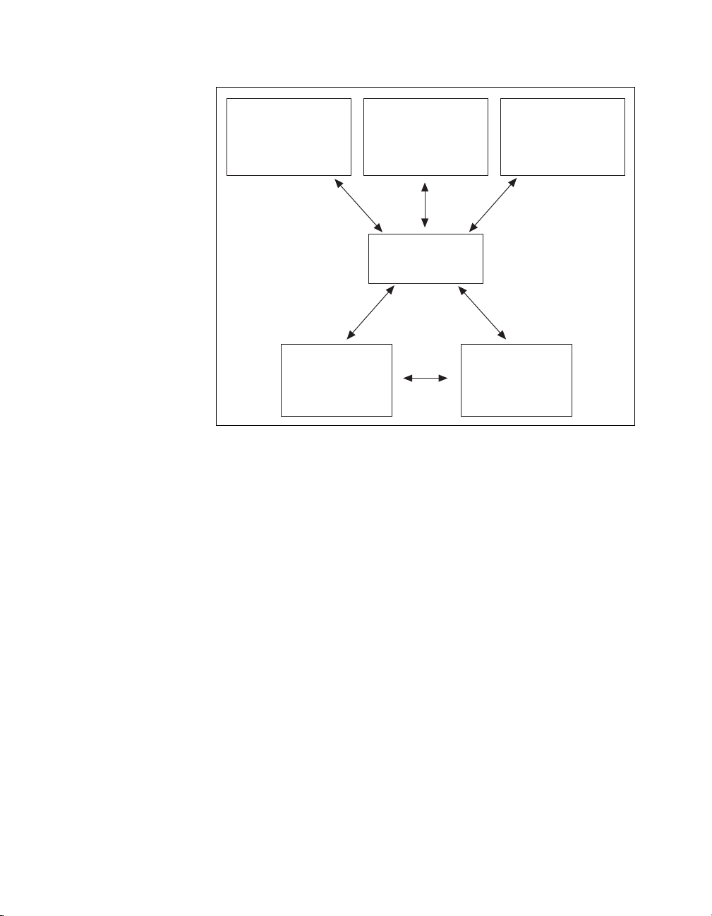
modifications to your code. Figure 1-1 illustrates the relationship between
NI-DAQ and LabVIEW and LabWindows/CVI. You can see that the data
acquisition parts of LabVIEW and LabWindows/CVI are functionally
equivalent to the NI-DAQ software.
© National Instruments Corporation 1-3 DAQCard-1200 User Manual
Page 15
Chapter 1 Introduction
Conventional
Programming
Environment
(PC, Macintosh, or
Sun SPARCstation)
Figure 1-1. The Relationship between the Programming Environment,
Register-Level Programming
The final option for programming any National Instruments DAQ
hardware is to write register-level software. Writing register-level
programming software can be very time-consuming and inefficient and is
not recommended.
DAQ or
SCXI Hardware
NI-DAQ, and Your Hardware
LabVIEW
(PC, Macintosh, or
Sun SPARCstation)
NI-DAQ
Driver Software
LabWindows/CVI
(PC or
Sun SPARCstation)
Personal
Computer
or
Workstation
Even if you are an experienced register-level programmer, consider using
NI-DAQ, LabVIEW, or LabWindows/CVI to program your National
Instruments DAQ hardware. Using the NI-DAQ, LabVIEW, or
LabWindows/CVI software is as easy and as flexible as register-level
programming and can save weeks of development time.
DAQCard-1200 User Manual 1-4 © National Instruments Corporation
Page 16

Optional Equipment
You can use the following National Instruments products with your
DAQCard-1200:
• BNC-2081
• CB-50 or CB-50LP I/O connector block with a 0.5 or 1.0 m cable
• ER-8, ER-16 electromechanical relays
• PR50-50F or PR50-50M cables
• SC-2042, SC-2043 strain gauge and RTD accessories
• SCXI products
For more information about optional equipment available from National
Instruments, refer to your National Instruments catalog or call the office
nearest you.
Unpacking
The DAQCard-1200 is shipped in an antistatic vinyl envelope; when you
are not using the DAQCard-1200, store it in this envelope.
Chapter 1 Introduction
Because the DAQCard-1200 is enclosed in a fully shielded case, no
additional electrostatic precautions are necessary. However, for your own
safety and to protect the DA QCard-1200, ne ver attempt to touch the pins of
the connectors.
© National Instruments Corporation 1-5 DAQCard-1200 User Manual
Page 17

Installation and Configuration
This chapter describes how to install and software configure the
DAQCard-1200.
Installation
There are two basic steps to installing the DAQCard-1200.
1. You must have Card & Socket Services 2.0 (or a later version) on your
computer.
2. Insert the DAQCard-1200 and attach the I/O cable.
The DAQCard-1200 has two connectors—a 68-pin PCMCIA bus
connector on one end and a 50-pin I/O connector on the other end. Insert
the PCMCIA bus connector into any available Type II PC Card slot until
the connector is seated firmly . Notice that the card is keye d so that it can be
inserted only one way. If your compu ter supports hot insertion, you may
insert or remove the D A QCard-1200 at any time, whether your computer is
powered on or off.
2
You can use either a 50-pin female or a 50-pin male cable to plug into the
DAQCard-1200. For more information on these products, see the Optional
Equipment section in Chapter 1, Introduction. Notice that the cable is
keyed so that you can insert it only one way. Be careful not to put strain
on the I/O cable when inserting it into and removing it from the
DA QCard-1200. Always grasp the cable b y the connector you are plugging
or unplugging. Never pull directly on the I/O cable to unplug it from the
DAQCard-1200.
The DA QCard-1200 is now installed. You are ready to make the appropriate
connections to the I/O connector cable as described in Chapter 3, Signal
Connections, and to install and configure your software.
© National Instruments Corporation 2-1 DAQCard-1200 User Manual
Page 18
Chapter 2 Installation and Configuration
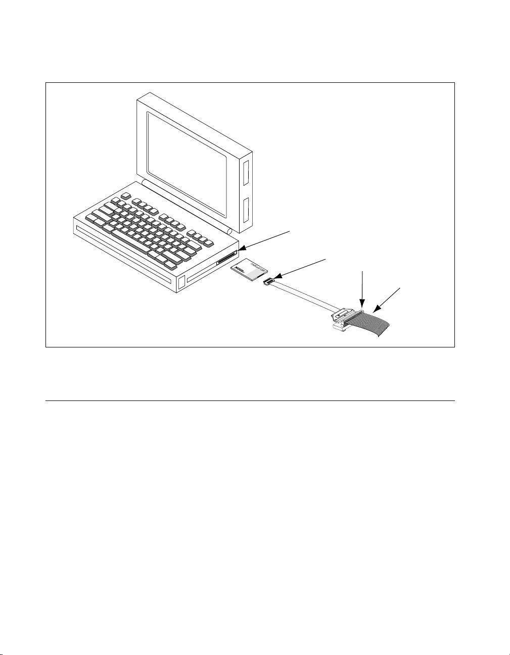
Figure 2-1 shows an example of a typical configuration.
Portable
Computer
PCMCIA Socket
I/O Cable
®
NATIONAL
INSTRUMENTS
The Software is the Instrument
CB-50
I/O Signals
Figure 2-1. A Typical Configuration for the DAQCard-1200
Configuration
The DAQCard-1200 is completely software configurable; refer to your
software manuals to install and configure your software.
If you are using NI-DAQ, refer to your NI-DAQ user manual or function
reference manual. The software installation and configuration instructions
are in Chapter 1. Find the installation and system configuration section for
your operating system and follow the instructions given there.
If you are using LabVIEW, you do not need the NI-DAQ manuals; the
software installation instructions are in your LabVIEW release notes. After
you have installed LabVIEW , refer to the Data Acquisition, VXI, and GPIB
Installation Notes section of Chapter 1, Required Configuration,
Installation, and Upgrade Information of your LabVIEW Version 5.1
Addendum for software configuration instructions.
DAQCard-1200 User Manual 2-2 © National Instruments Corporation
Page 19
If you are using LabWindows/CVI, the software installation instructions
are in Part 1, Introduction to LabWindows/CVI, of the Getting Started with
LabWindows/CVI manual. After you have installed LabWindows/CVI,
refer to Chapter 1, Configuring LabWindows/CVI, of the LabWindows/CVI
User Manual for software configuration instructions. Then follow
DAQ configuration instructions in your NI-DAQ user manual.
Analog Input Configuration
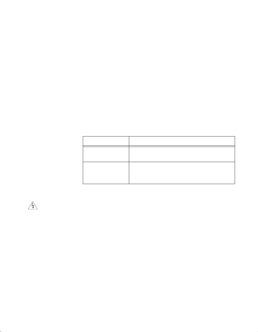
At startup, the DAQCard-1200 defaults to the following configuration:
• Referenced single-ended input mode
• ±5 V analog input range
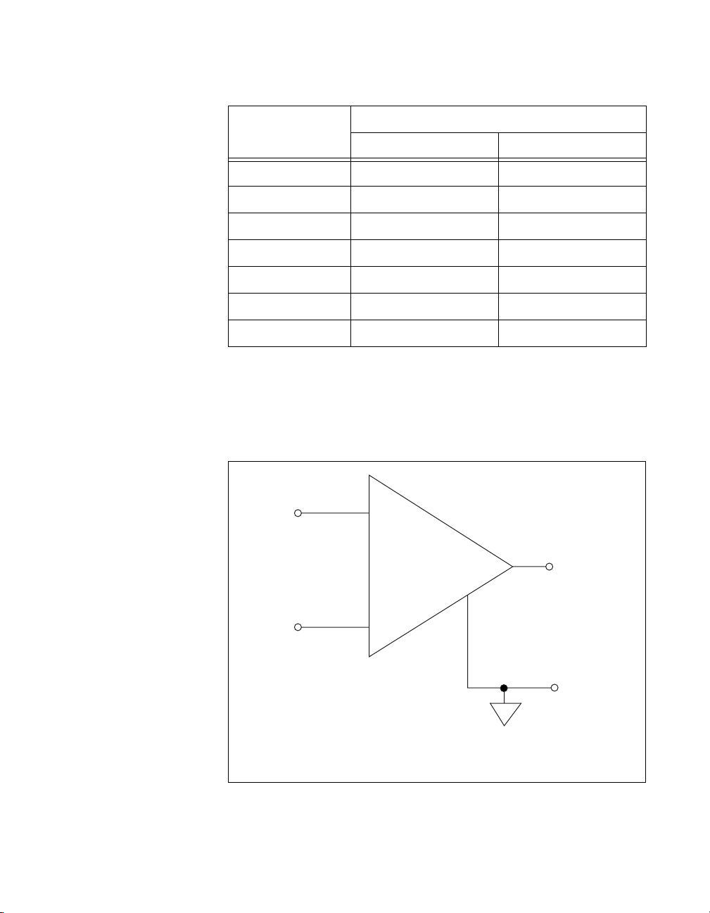
Table 2-1 lists the available analog I/O configurations for the
DAQCard-1200 and shows the default settings.
Chapter 2 Installation and Configuration
Warning
Table 2-1.
Analog I/O Settings
Parameter Configuratio n
Analog Input Polarity
Bipolar—±5 V (default setting)
Unipolar—0–10 V
Analog Input Mode Referenced single-ended (RSE) (default setting)
Non-referenced single-ended (NRSE)
Differential (DIFF)
The analog input circuitry is software configurable.
Connections, including power signals to ground and vice versa, that exceed any of
the maximum signal ratings on the DAQCard-1200 can damage your card and
computer . National Instruments is
NOT
liable for any damages or injuries resulting
from incorrect signal connections.
Analog Input Polarity
You can select the analog input on the DAQCard-1200 for either a unipolar
range (0 to 10 V) or a bipolar range (–5 to +5 V). If you select a bipolar
range, the two’s complement coding is selected. In this mode, –5 V input
corresponds to F800 hex (–2,048 decimal) and +5 V corresponds to
7FF hex (2,047 decimal). If you select a unipolar mode, the straight binary
coding is selected. In this mode, 0 V input corresponds to 0 hex, and +10 V
corresponds to FFF hex (4,095 decimal).
© National Instruments Corporation 2-3 DAQCard-1200 User Manual
Page 20

Chapter 2 Installation and Configuration
Analog Input Mode
The DAQCard-1200 has three different input modes—referenced
single-ended (RSE), non-referenced single-ended (NRSE), and differential
(DIFF). Single-ended configuration provides eight input channels. DIFF
configuration provides four input channels. Table 2-2 describes these
configurations.
Table 2-2.
Analog
Input Modes
RSE Referenced single-ended mode provides eight single-ended inputs with the
negative input of the instrumentation amplifier referenced to AISENSE/AIGND,
which is tied to ground through about 200 Ω resistance (default setting).
NRSE Non-referenced single-ended configuration provides eight single-ended inputs
with the negative input of the instrumentation amplifier tied to AISENSE/AIGND
and not connected to ground.
DIFF Differential mode provides four differential inputs with the positive input of the
instrumentation amplifier tied to channels 0, 2, 4, or 6 and the negative input tied
to channels 1, 3, 5, or 7, respectively , thus pairing channels (0, 1), (2,3), (4,5), (6,7).
While reading the following paragraphs, you may find it helpful to refer to
the Analog Input Signal Connections section of Chapter 3, Signal
Connections, which contains diagrams showing the signal paths for the
three configurations. These three modes are software selectable.
Analog Input Modes for the DAQCard-1200
Description
RSE Input (Eight Channels, Default Setting)
RSE input means that all input signals are referenced to a common ground
point that is also tied to the DAQCard-1200 analog input ground. The RSE
configuration is useful for measuring floating signal sources. See the Types
of Signal Sources section of Chapter 3, Signal Connections, for more
information. With the RSE configuration, the DAQCard-1200 can monitor
eight different analog input channels.
Considerations for using the RSE configuration are discussed in Chapter 3,
Signal Connections. Notice that in RSE mode, the return path of the
signal is through analog ground at the connector through the
AISENSE/AIGND pin.
DAQCard-1200 User Manual 2-4 © National Instruments Corporation
Page 21

Chapter 2 Installation and Configuration
NRSE Input (Eight Channels)
NRSE input means that all signals are referenced to the same common
mode voltage, which is allowed to float with respect to the analog ground
of the DAQCard-1200. This common mode voltage is subsequently
subtracted out by the instrumentation amplifier. NRSE configuration is
useful when measuring ground-referenced signal sources.
Considerations in using the NRSE configuration are discussed in
Chapter 3, Signal Connections. Notice that in this mode, the return path of
the signal is through the negative terminal of the amplif ier, available at the
connector through the pin AISENSE/AIGND.
DIFF Input (Four Channels)
DIFF input means that each input signal has its own reference, and the
difference between each signal and its reference is measured. The signal
and its reference are each assigned an input channel. With DIFF input
configuration, the DAQCard-1200 can monitor four different analog input
signals.
Considerations for using the DIFF configuration are discussed in
Chapter 3, Signal Connections. Notice that the signal return path is through
the negative terminal of the instrumentation amplifier and through
channel 1, 3, 5, or 7 depending on which channel pair you select.
Analog Output Configuration
You can set the analog output on the DAQCard-1200 to either bipolar or
unipolar configurations.
Parameter Configuration
Analog Output CH0 Polarity Bipolar—±5 V (default setting)
Unipolar—0–10 V
Analog Output CH1 Polarity Bipolar—±5 V (default setting)
Unipolar—0–10 V
© National Instruments Corporation 2-5 DAQCard-1200 User Manual
Page 22

Chapter 2 Installation and Configuration
Analog Output Polarity
The DAQCard-1200 has two channels of analog output voltage at the front
panel I/O connector. You can configure each analog output channel for
either unipolar or bipolar output. A unipolar configuration has a range of
0 to 10 V at the analog output. A bipolar configuration has a range of –5 to
+5 V at the analog output. If you select a bipolar range for a D/A conversion
(DAC), the two’s complement coding is selected. In this mode, data values
written to the analog output channel range from F800 hex (–2,048 decimal)
to 7FF hex (2,047 decimal). If you select a unipolar range for a DAC, you
are selecting the straight binary coding. In this mode, data values written to
the analog output channel range from 0 to FFF hex (4,095 decimal).
Digital I/O Configuration
The DAQCard-1200 uses the MSM82C55 programmable peripheral
interface (PPI). This chip provides 24 digital lines in the form of
three ports—A, B, and C. On power up, all three ports reset to high
impedance inputs. For information about configuring the MSM82C55,
see the DAQ Timing Connections section of Chapter 3, Signal
Connections.
Caution
!
The DAQCard-1200 DIO lines are not pulled up or pulled down. If you are using
these lines as digital outputs, add 10 k
your application) to the DIO line(s) you are using.
Counter Configuration
You can use the MSM82C53A counter/timers for general-purpose timing
applications, such as pulse and square wave generation, event counting,
and pulse-width, time-lapse, and frequency measurement. For information
about configuring the MSM82C53A, see the DAQ Timing Connections
section of Chapter 3, Signal Connections.
ΩΩΩΩ
resistors to +5 V or DGND (depending on
DAQCard-1200 User Manual 2-6 © National Instruments Corporation
Page 23

Signal Connections
This chapter describes the signals on the DAQCard-1200 I/O connector.
I/O Connector
Figure 3-1 shows the pin assignments for the DAQCard-1200 I/O
connector. This connector is attached to the ribbon cable that extends from
the PC Card slot when the card is installed and the cable connected.
3
Warning
Connections, including power signals to ground and vice versa, that exceed any of
the maximum ratings of input or output signals on the DAQCard-1200 can
damage the DA QCard-1200 and the PC. National Instruments is
damages resulting from any such signal connections.
NOT
liable for any
© National Instruments Corporation 3-1 DAQCard-1200 User Manual
Page 24
Chapter 3 Signal Connections
ACH0
ACH2
ACH4
ACH6
AISENSE/AIGND
AGND
DGND
PA1
PA3
PA5
PA7
PB1
PB3
PB5
PB7
PC1
PC3
PC5
PC7
EXTUPDATE*
OUTB0
OUTB1
CLKB1
GATB2
+5 V
12
34
56
78
910
11 12
13 14
15 16
17 18
19 20
21 22
23 24
25 26
27 28
29 30
31 32
33 34
35 36
37 38
39 40
41 42
43 44
45 46
47 48
49 50
ACH1
ACH3
ACH5
ACH7
DAC0OUT
DAC1OUT
PA0
PA2
PA4
PA6
PB0
PB2
PB4
PB6
PC0
PC2
PC4
PC6
EXTTRIG
EXTCONV*
GATB0
GATB1
OUTB2
CLKB2
DGND
Figure 3-1. DAQCard-1200 I/O Connector Pin Assignments
DAQCard-1200 User Manual 3-2 © National Instruments Corporation
Page 25

Signal Connection Descriptions
The following table describes the connector pins on the DAQCard-1200
front I/O connector by pin number and gives the signal name and the
significance of each signal connector pin.
Pins Signal Name Direction Reference Description
Chapter 3 Signal Connections
1–8 ACH<0..7> AI AGND Analog Channel 0 through 7—Analog input channels 0
9 AISENSE/AIGND AI AGND Analog Input Sense/Analog Input Ground—Connected to
10 DAC0OUT AO AGND DAC0 Output—Voltage output signal for analog output
11 AGND N/A N/A Analog Ground—Analog output ground reference for
12 DAC1OUT AO AGND DAC1 Output—Voltage output signal for analog output
13 DGND N/A N/A Digital Ground—Voltage ground reference for the digital
14–21 PA<0..7> DIO DGND Port A 0 through 7—Bidirectional data lines for port A.
22–29 PB<0..7> DIO DGND Port B 0 through 7—Bidirectional data lines for port B.
30–37 PC<0..7> DIO DGND Port C 0 through 7—Bidirectional data lines for port C.
38 EXTTRIG DI DGND External Trigger—External control signal to trigger a
39 EXTUPDATE* DI DGND External Update—External control signal to update
through 7.
AGND in RSE mode, analog input sense in NRSE mode.
channel 0.
analog output voltages. This signal is the bias current return
point for differential measurements.
channel 1.
signals and the +5 V supply.
PA7 is the MSB, and PA0 is the LSB.
PB7 is the MSB, and PB0 is the LSB.
PC7 is the MSB, and PC0 is the LSB.
DAQ operation.
DAC outputs.
40 EXTCONV* DIO DGND External Convert—External control signal to time
41 OUTB0 DO DGND Output B0—Voltage output signal of counter B0.
42 GATB0 DI DGND Gate B0—External control signal for gating counter B0.
43 OUTB1 DIO DGND Output B1—Voltage output signal of counter B1 when
44 GATB1 DI DGND Gate B1—External control signal for gating counter B1.
© National Instruments Corporation 3-3 DAQCard-1200 User Manual
A/D conversions (DI) and drive SCANCLK when you use
SCXI (DO).
selected as output (DO). This is the external control signal
for timing an interval cycle when selected as input (DI).
Page 26

Chapter 3 Signal Connections
Pins Signal Name Direction Reference Description
45 CLKB1 DI DGND Clock B1—External control clock signal for counter B1.
46 OUTB2 DO DGND Counter B2—Voltage output signal of counter B2.
47 GATB2 DI DGND Gate B2—External control signal for gating counter B2.
48 CLKB2 DI DGND Clock B2—External control clock signal for counter B2.
49 +5 V DO DGND +5 Volts—Fused for up to 1 A of +5 V supply, but limit
current to 250 mA.
50 DGND N/A N/A Digital Ground—Voltage ground reference for the digital
signals and the +5 V supply.
*Indicates that the signal is active low.
AI = Analog Input DI = Digital Input DIO = Digital Input/Output
AO = Analog Output DO = Digital Output N/A = Not Applicable
The connector pins are grouped into analog input signal pins, analog output
signal pins, digital I/O signal pins, timing I/O signal pins, and power
connections. Signal connection guidelines for each of these groups are
described in the following sections.
Analog Input Signal Connections
Pins 1 through 8 are analog input signal pins for the 12-bit ADC. Pin 9,
AISENSE/AIGND, is an analog common signal. You can use this pin as a
signal ground connection to the DAQCard-1200 in RSE mode, or as a
return path in NRSE mode. Pin 11, AGND, is the bias current return point
for differential measurements. Pins 1 through 8 are tied, through 4.7 kΩ
series resistances, to the eight single-ended analog input channels of the
input multiplexer. Pins 2, 4, 6, and 8 are also tied to an input multiplexer
for DIFF mode.
The signal ranges for inputs ACH<0..7> at all possible gains are shown in
Table 3-1. Exceeding the input signal range will not damage the input
circuitry as long as the maximum input voltage rating of ±35 V powered on
and ±25 V powered off is not e xceeded. The D AQCard-1200 is guaranteed
to withstand inputs up to the maximum input voltage rating.
Warning
Exceeding the input signal range distorts input signals. Exceeding the maximum
input voltage rating may damage the DAQCard-1200 and the computer. National
Instruments is
DAQCard-1200 User Manual 3-4 © National Instruments Corporation
NOT
liable for any damages resulting from such signal connections.
Page 27
Chapter 3 Signal Connections
Table 3-1. Bipolar and Unipolar Analog Input Signal Range Versus Gain
Input Signal Range
Gain Setting
Bipolar Unipolar
1 ±5 V 0 to 10 V
2 ±2.5 V 0 to 5 V
5 ±1 V 0 to 2 V
10 ±500 mV 0 to 1 V
20 ±250 mV 0 to 500 mV
50 ±100 mV 0 to 200 mV
100 ±50 mV 0 to 100 mV
How you connect analog input signals to the DAQCard-1200 depends on
how you configure the card analog input circuitry and the type of input
signal source. With different DAQCard-1200 configurations, you can use
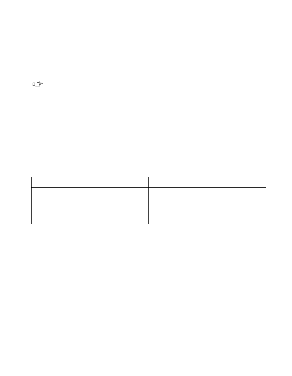
the instrumentation amplifier in different ways. Figure 3-2 shows a diagram
of the DAQCard-1200 instrumentation amplifier.
Instrumentation
+
V
in
+
Amplifier
+
–
V
in
–
V
m
Measured
Voltage
–
V
= [Vin + – Vin –] GAIN
m
Figure 3-2. DAQCard-1200 Instrumentation Amplifier
© National Instruments Corporation 3-5 DAQCard-1200 User Manual
Page 28

Chapter 3 Signal Connections
The instrumentation amplifier applies gain, common-mode voltage
rejection, and high-input impedance to the analog input signals connected
to the DAQCard-1200. Signals are routed to the positive and negative
inputs of the instrumentation amplifier through input multiplexers on the
DAQCard-1200. The instrumentation amplifier converts two input signals
to a signal that is the difference between the two input signals multiplied by
the gain setting of the amplifier. The amplif ier output v oltage is referenced
to the DAQCard-1200 ground. The DAQCard-1200 ADC measures this
output voltage when it performs A/D conversions.
All signals must be referenced to ground, either at the source device or at
the DAQCard-1200. If you have a floating source, you must use a
ground-referenced input connection at the DAQCard-1200. If you have a
grounded source, you must use a nonreferenced input connection at the
DAQCard-1200.
Types of Signal Sources
When configuring the input mode of the DAQCard-1200 and making
signal connections, you must first determine whether the signal source is
floating or ground referenced. This section describes these two types of
signals.
Floating Signal Sources
A floating signal source is not connected in any way to the building ground
system but has an isolated ground-reference point. Some examples of
floating signal sources are outputs of transformers, thermocouples,
battery-powered devices, optical isolator outputs, and isolation amplifiers.
You must tie the ground reference of a floating signal to the
DAQCard-1200 analog input ground to establish a local or onboard
reference for the signal. Otherwise, the measured input signal varies or
appears to float. An instrument or device that supplies an isolated output
falls into the floating signal source category.
Ground-Referenced Signal Sources
A ground-referenced signal source is connected in some way to the
building system ground and is therefore already connected to a common
ground point with respect to the DAQCard-1200, assuming that the PC is
plugged into the same power system. Nonisolated outputs of instruments
and devices that plug into the building power system fall into this category.
DAQCard-1200 User Manual 3-6 © National Instruments Corporation
Page 29
Chapter 3 Signal Connections
The difference in ground potential between two instruments connected to
the same building power system is typically between 1 mV and 100 mV but
can be much higher if power distribution circuits are not properly
connected. The connection instructions that follow for grounded signal
sources eliminate this ground potential difference from the measured
signal.
Note If you power both the DA QCard-1200 and your PC with a floating power source,
such as a battery, your system may be floating with respect to earth ground. In this
case, treat all of your signal sources as floating sources.
Input Configurations
You can configure the DAQCard-1200 for one of three input modes—RSE,
NRSE, or DIFF. The following sections discuss the use of single-ended and
differential measurements, and considerations for measuring both floating
and ground-referenced signal sources. Table 3-2 summarizes the
recommended input configurations for both types of signal sources.
Table 3-2. Recommended Input Configurations for Ground-Referenced
and Floating Signal Sources
Type of Signal Recommended Input Configuration
Ground-Referenced
(nonisolated outputs, plug-in instruments)
Floating
(batteries, thermocouples, isolated outputs)
DIFF with bias resistors
DIFF
NRSE
RSE
Differential Connection Considerations (DIFF Configuration)
Differential connections are those in which each DAQCard-1200 analog
input signal has its own reference signal or signal return path. These
connections are available when you configure the DAQCard-1200 in
the DIFF mode. Each input signal is tied to the positive input of th e
instrumentation amplifier, and its reference signal, or return, is tied to
the negative input of the instrumentation ampli fi e r.
© National Instruments Corporation 3-7 DAQCard-1200 User Manual
Page 30

Chapter 3 Signal Connections
When you configure the DAQCard-1200 for DIFF input, each signal uses
two of the multiplexer inputs—one for the signal and one for its reference
signal. Therefore, only four analog input channels are available when using
the DIFF configuration. You should use the DIFF input configuration when
any of the following conditions is present:
• Input signals are low level (less than 1 V).
• Leads connecting the signals to the DAQCard-1200 are greater
than 15 ft.
• Any of the input signals requires a separate ground-reference point or
return signal.
• The signal leads travel through noisy environments.
Differential signal connections reduce picked-up noise and increase
common-mode signal and noise rejection. With these connections, input
signals can float within the common-mode limits of the input
instrumentation amplifier.
Differential Connections for Grounded Signal Sources
Figure 3-3 shows how to connect a ground-referenced signal source to a
DAQCard-1200 configured for DIFF input. Refer to the Analog Input
Configuration section in Chapter 2, Installation and Configuration, for
configuration instructions.
DAQCard-1200 User Manual 3-8 © National Instruments Corporation
Page 31

Grounded
Signal
Source
Common-Mode
Noise,
Ground
Potential
Chapter 3 Signal Connections
ACH 0
1
ACH 2
3
ACH 4
+
V
s
–
+
V
cm
–
5
ACH 6
7
ACH 1
2
ACH 3
4
ACH 5
6
ACH 7
8
+
+
m
Measured
Voltage
–
–
V
AGND
11
Front I/O Connector
DAQCard-1200 in DIFF Configuration
Figure 3-3. Differential Input Connections for Grounded Signal Sources
With this type of connection, the instrumentation amplifier rejects both the
common-mode noise in the signal and the ground-potential difference
between the signal source and the DA QCard-1200 ground, which is shown
as V
in Figure 3-3.
cm
Differential Connections for Floating Signal Sources
Figure 3-4 shows how to connect a floating signal source to a
DAQCard-1200 that is configured for DIFF input. Configuration
instructions are included in the Analog Input Configuration section of
Chapter 2, Installation and Configuration.
© National Instruments Corporation 3-9 DAQCard-1200 User Manual
Page 32

Chapter 3 Signal Connections
Floating
Signal
Source
+
V
s
–
ACH 0
1
ACH 2
3
ACH 4
5
ACH 6
7
+
100 kΩ
Bias
Current
Return
Paths
Front I/O Connector
100 kΩ
ACH 1
2
ACH 3
4
ACH 5
6
ACH 7
8
AGND
11
DAQCard-1200 in DIFF Configuration
–
+
Measured
V
m
Voltage
–
Figure 3-4. Differential Input Connections for Floating Sources
The 100 kΩ resistors shown in Figure 3-4 create a return path to ground for
the bias currents of the instrumentation amplifier . If there is no return path,
the instrumentation amplifier bias currents charge stray capacitances,
resulting in uncontrollable drift and possible saturation in the amplifier.
A resistor from each input to ground, as shown in Figure 3-4, provides bias
current return paths for an AC-coupled input signal.
If the input signal is DC-coupled, you need only the resistor that connects
the negative signal input to ground. This connection does not lower the
input impedance of the analog input channel.
DAQCard-1200 User Manual 3-10 © National Instruments Corporation
Page 33

Chapter 3 Signal Connections
Single-Ended Connection Considerations
Single-ended connections are those in which all DAQCard-1200 analog
input signals are referenced to one common ground. The input signals are
tied to the positive input of the instrumentation amplifier, and their
common ground point is tied to the negative input of the instrumentation
amplifier.
When the DAQCard-1200 is configured for single-ended input (NRSE or
RSE), eight analog input channels are available. You can use single-ended
input connections when the following criteria are met by all input signals:
• Input signals are high level (greater than 1 V).
• Leads connecting the signals to the DAQCard-1200 are less than 15 ft.
• All input signals share a common reference signal (at the source).
If any of the preceding criteria is not met, you should use DIFF input
configuration.
You can software configure the DAQCard-1200 for two different types of
single-ended connections, RSE configuration and NRSE configuration.
Use the RSE configuration for floating signal sources; in this case, the
DA QCard-1200 provides the reference ground point for the external signal.
Use the NRSE configuration for ground-referenced signal sources; in this
case, the external signal supplies its own reference ground point and the
DAQCard-1200 should not supply one.
Single-Ended Connections for Floating Signal Sources
(RSE Configuration)
Figure 3-5 shows how to connect a floating signal source to a
DAQCard-1200 configured for single-ended input. You must configure the
DAQCard-1200 analog input circuitry for RSE input to make these types
of connections. For configuration instructions, refer to the Analog Input
Configuration section of Chapter 2, Installation and Configuration.
© National Instruments Corporation 3-11 DAQCard-1200 User Manual
Page 34

Chapter 3 Signal Connections
Floating
Signal
Source
+
V
s
ACH 0
1
ACH 1
2
ACH 2
3
ACH 7
8
+
–
Front I/O Connector
AISENSE/AIGND
9
AGND
11
DAQCard-1200 in RSE Configuration
–
+
m
Measured
Voltage
–
V
Figure 3-5. Single-Ended Input Connections for Floating Signal Sources
Single-Ended Connections for Grounded Signal Sources
(NRSE Configuration)
If you measure a grounded signal source with a single-ended configuration,
you must configure the DAQCard-1200 in the NRSE input configuration.
The signal is connected to the positive input of the DAQCard-1200
instrumentation amplifier and the signal local ground reference is
connected to the negative input of the DAQCard-1200 instrumentation
amplifier. Therefore, you must connect the ground point of the signal to the
AISENSE pin. Any potential difference between the DAQCard-1200
ground and the signal ground appears as a common-mode signal at both the
positive and negative inputs of the instrumentation amplifier and is
therefore rejected by the amplifier. On the other hand, if the input circuitry
of the DAQCard-1200 is referenced to ground, such as in the RSE
configuration, this difference in ground potentials appears as an error in the
measured voltage.
Figure 3-6 shows how to connect a grounded signal source to a
DAQCard-1200 configured in the NRSE configuration. For configuration
instructions, see the Analog Input Configuration section in Chapter 2,
Installation and Configuration.
DAQCard-1200 User Manual 3-12 © National Instruments Corporation
Page 35

GroundReferenced
Signal
Source
Common-Mode
Noise
Chapter 3 Signal Connections
ACH 0
1
ACH 1
2
ACH 2
+
V
s
–
+
V
cm
–
3
+
ACH 7
8
9
AGND
11
AISENSE/AIGND
–
V
m
+
Measured
Voltage
–
Front I/O Connector
DAQCard-1200 in NRSE Input Configuration
Figure 3-6. Single-Ended Input Connections for Grounded Signal Sources
Common-Mode Signal Rejection Considerations
Figures 3-3 and 3-6 show connections for signal sources that are already
referenced to some ground point with respect to the DAQCard-1200. In
these cases, the instrumentation amplifier can reject any voltage caused by
ground-potential differences between the signal source and the
DAQCard-1200. In addition, with differential input connections, the
instrumentation amplifier can reject common-mode noise pickup in the
leads connecting the signal sources to the DAQCard-1200.
The common-mode input range of the DAQCard-1200 instrumentation
amplifier is the magnitude of the greatest common-mode signal that can be
rejected.
The common-mode input range for the DA QCard-1200 depends on the size
of the differential input signal (V
instrumentation amplifier. In unipolar mode, the differential input range is
0 to 10 V. In bipolar mode, the differential input range is –5 to +5 V.
V
should remain within a range of –6 to 6 V in bipolar mode and –6 to
–
in
diff
= V
in+
– V
) and the gain setting of the
in–
© National Instruments Corporation 3-13 DAQCard-1200 User Manual
Page 36

Chapter 3 Signal Connections
2 V in unipolar mode. V
either mode.
Analog Output Signal Connections
Pins 10 through 12 of the front connector are the analog output signals
DAC0OUT, AGND, and DAC1OUT.
DAC0OUT is the voltage output signal for analog output channel 0.
DA C1OUT is the voltage output signal for analog output channel 1. A GND
is the ground-reference point for both analog output channels and analog
input.
The following output ranges are available:
• Output signal range
Bipolar output ±5 V*
–
Unipolar output 0 to 10 V*
–
*
Maximum load current ±1 mA for 12-bit linearity (per DAC)
Figure 3-7 shows how to make analog output signal connections.
should remain within a range of –6 to +11 V in
+
in
10 DAC0OUT
+
Load
Load
DAQCard-1200 User Manual 3-14 © National Instruments Corporation
VOUT 0
VOUT 1
Front I/O Connector
–
–
+
11
12
AGND
DAC1OUT
Figure 3-7.
Analog Output Channels
Analog Output Signal Connections
Channel 0
Channel 1
DAQCard-1200
Page 37

Digital I/O Signal Connections
Chapter 3 Signal Connections
Caution
!
The DAQCard-1200 DIO lines are not pulled up or pulled down. If you are using
these lines as digital outputs, add 10 k
your application) to the DIO line(s) you are using.
Pins 13 through 37 of the front connector are digital I/O signal pins.
Digital I/O on the DAQCard-1200 uses the 82C55A integrated circuit.
The 82C55A is a general-purpose peripheral interface containing
24 programmable I/O pins. These pins represent the three 8-bit ports
(PA, PB, and PC) of the 82C55A.
Pins 14 through 21 are connected to the digital lines PA<0..7 > for
digital I/O port A. Pins 22 through 29 are connected to the digital lines
PB<0..7> for digital I/O port B. Pins 30 through 37 are connected to the
digital lines PC<0..7> for digital I/O port C. Pin 13, DGND, is the digital
ground pin for all three digital I/O ports. Refer to Appendix A,
Specifications, for signal voltage and current specifications.
ΩΩΩΩ
resistors to +5 V or DGND (depending on
© National Instruments Corporation 3-15 DAQCard-1200 User Manual
Page 38

Chapter 3 Signal Connections
Figure 3-8 illustrates signal connections for three typical digital I/O
applications.
Port C
PC <0..7>
22 PB0
+5 V
LED
TTL Signal
29 PB7
13
+5 V
DGND
30 PA0
I/O Connector
DAQCard-1200
Port B
PB <0..7>
Port A
PA <0..7>
Figure 3-8. Digital I/O Connections
In Figure 3-8, port A is configured for digital output, and ports B and C are
configured for digital input. Digital input applications include receiving
TTL signals and sensing external device states such as the switch in
Figure 3-8. Digital output applications include sending TTL signals and
driving external devices such as the LED shown in Figure 3-8.
DAQCard-1200 User Manual 3-16 © National Instruments Corporation
Page 39

Chapter 3 Signal Connections
Port C Pin Connections
The signals assigned to port C depend on how the 82C55A is configured.
In mode 0 or no handshaking configuration, port C is configured as
two 4-bit I/O ports. In modes 1 and 2, or handshaking configuration, port C
is used for status and handshaking signals with zero, two, or three lines
available for general-purpose I/O. Table 3-3 summarizes the port C signal
assignments for each configuration.
Note
Table 3-3 shows both the port C signal assignments and the terminology
correlation between different documentation sources. The 82C55A terminology
refers to the different 82C55A configurations as modes, whereas NI-DAQ and
LabVIEW documentation refers to them as handshaking and no handshaking.
These signal assignments are the same for all four 82C55A PPIs.
Table 3-3.
Configuration Terminology Signal Assignments
82C55A/
DAQCard-1200
User Manual
Mode 0
(Basic I/O)
Mode 1
(Strobed Input)
Mode 1
(Strobed Output)
Mode 2
(Bidirectional Bus)
*Indicates that the signal is active low.
Subscripts A and B denote port A or port B handshaking signals.
NI-DAQ/
LabVIEW
No
Handshaking
Handshaking I/O I/O IBFASTBA* INTRASTBB* IBFBBINTR
Handshaking OBFA* ACKA* I/O I/O INTRAACKB* OBFB* INTR
Handshaking OBFA* ACKA* IBFASTBA* INTR
PC7 PC6 PC5 PC4 PC3 PC2 PC1 PC0
I/O I/O I/O I/O I/O I/O I/O I/O
Port C Signal Assignments
I/O I/O I/O
A
B
B
© National Instruments Corporation 3-17 DAQCard-1200 User Manual
Page 40

Chapter 3 Signal Connections
Timing Specifications
Use the handshaking lines STB* and IBF to synchronize input transfers.
Use the handshaking lines OBF* and ACK* to synchronize output
transfers.
The following signals are used in the timing diagrams shown later in this
chapter:
Name Type Description
STB* Input Strobe Input—A low signal on this handshaking line loads data into the
input latch.
IBF Output Input Buffer Full—A high signal on this handshaking line indicates that
data has been loaded into the input latch. This is primarily an input
acknowledge signal.
ACK* Input Acknowledge Input—A low signal on this handshaking line indicates
that the data written from the specified port has been accepted. This
signal is primarily a response from the external device that it has
received the data from the DA QCard-1200.
OBF* Output Ou tpu t Buffer Full—A low signal on this handshaking line indicates
that data has been written from the specified port.
INTR Output Interrup t Request—This signal becomes high when the 82C55A
requests service during a data transfer. Set the appropriate interrupt
enable signals to generate this signal.
RD* Internal Read—This signal is the read signal generated from the parallel port
interface circuitry.
WRT* Internal Write—This signal is the write signal generated from the parallel port
interface circuitry.
DA T A Bidirectional Data Lines at the Specified Port—This signal indicates when the data
on the data lines at a specified port is or should be available.
DAQCard-1200 User Manual 3-18 © National Instruments Corporation
Page 41

STB *
Chapter 3 Signal Connections
Mode 1 Input Timing
Figure 3-9 shows the timing specifications for an input transfer in mode 1.
T1
T2 T4
T7
IBF
INTR
RD *
T3 T5
DATA
T6
Name Description Minimum Maximum
T1 STB* pulse width 100 —
T2 STB* = 0 to IBF = 1 — 150
T3 Data before STB* = 1 20 —
T4 STB* = 1 to INTR = 1 — 150
T5 Data after STB* = 1 50 —
T6 RD* = 0 to INTR = 0 — 200
T7 RD* = 1 to IBF = 0 — 150
All timing values are in nanoseconds.
Figure 3-9.
© National Instruments Corporation 3-19 DAQCard-1200 User Manual
Mode 1 Timing Specifications for Input Transfers
Page 42

Chapter 3 Signal Connections
WRT*
Mode 1 Output Timing
Figure 3-10 shows the timing specifications for an output transfer in
mode 1.
T3
T4
OBF*
INTR
ACK*
DATA
T1
T6
T5
T2
Name Description Minimum Maximum
T1 WRT* = 0 to INTR = 0 — 250
T2 WRT* = 1 to output — 200
T3 WRT* = 1 to OBF* = 0 — 150
T4 ACK* = 0 to OBF* = 1 — 150
T5 ACK* pulse width 100 —
T6 ACK* = 1 to INTR = 1 — 150
All timing values are in nanoseconds.
Figure 3-10.
Mode 1 Timing Specifications for Output Transfers
Mode 2 Bidirectional Timing
Figure 3-11 shows the timing specification s for bidirectional transfers in
mode 2.
DAQCard-1200 User Manual 3-20 © National Instruments Corporation
Page 43

T1
Chapter 3 Signal Connections
WRT *
OBF *
INTR
ACK *
STB *
IBF
RD *
DATA
T3
T4
T2 T5 T8 T9
T6
T7
T10
Name Description Minimum Maximum
T1 WRT* = 1 to OBF* = 0 — 150
T2 Data before STB* = 1 20 —
T3 STB* pulse width 100 —
T4 STB* = 0 to IBF = 1 — 150
T5 Data after STB* = 1 50 —
T6 ACK* = 0 to OBF = 1 — 150
T7 ACK* pulse width 100 —
T8 ACK* = 0 to output — 150
T9 ACK* = 1 to output float 20 250
T10 RD* = 1 to IBF = 0 — 150
All timing values are in nanoseconds.
Figure 3-11. Mode 2 Timing Specifications for Bidirectional Transfers
© National Instruments Corporation 3-21 DAQCard-1200 User Manual
Page 44

Chapter 3 Signal Connections
DAQ and General-Purpose Timing Signal Connections
Pins 38 through 48 of the front connector are connections for timing
I/Osignals. The DAQCard-1200 timing I/O uses two 82C53 counter/timer
integrated circuits. One circuit, designated 82C53(A), is used exclusively
for DAQ timing, and the other, 82C53(B), is available for general use.
Youcan use pins 38 through 40 and pin 43 to carry external signals for
DAQ timing in place of the dedicated 82C53(A). These signals are
explained in the next section, DAQ Timing Connections. Pins 41 through
48 carry general-purpose timing signals from 82C53(B). These signals are
explained in the General-Purpose Timing Signal Connections section later
in this chapter.
DAQ Timing Connections
Each 82C53 counter/timer circuit contains three counters. Counter 0 on the
82C53(A) counter/timer, referred to as A0, is a sample-interval counter in
timed A/D conversions. Counter 1 on the 82C53(A) counter/timer, referred
to as A1, is a sample counter in controlled A/D conversions. Therefore,
counter A1 stops data acquisition after a predefined number of samples.
These counters are not available for general use.
Instead of counter A0, you can use EXTCONV* to externally time
conversions. Figure3-12 shows the timing requirements for the
EXTCONV* input. A falling edge on the EXTCONV* initiates an
A/Dconversion.
t
w
tw 250 ns minimum
EXTCONV* Signal Timing
EXTCONV*
V
IH
t
V
IL
w
A/D Conversion starts within
125 ns from this point.
Figure 3-12.
The external control signal EXTTRIG can either start a data acquisition
sequence or terminate an ongoing data acquisition sequence depending on
the mode—posttrigger or pretrigger. These modes are software selectable.
DAQCard-1200 User Manual 3-22 © National Instruments Corporation
Page 45

EXTTRIG
Chapter 3 Signal Connections
In the posttrigger mode, EXTTRIG serves as an external trigger that
initiates a data acquisition sequence. When you use counter A0 to time
sample intervals, a rising edge on EXTTRIG starts counter A0 and the data
acquisition sequence. When you use EXTCONV* to time sample intervals,
data acquisition is enabled on a rising edge of EXTTRIG followed by a
rising edge on EXTCONV*. The first con version occurs on the next falling
edge of EXTCONV*. Further transitions on the EXTTRIG line have no
effect until a new data acquisition sequence is established.
Figure 3-13 shows a possible controlled data acquisition sequence using
EXTCONV* and EXTTRIG. The rising edge of EXTCONV* that enables
external conversions must occur a minimum of 50 ns after the rising edge
of EXTTRIG. The first conversion occurs on the next falling edge of
EXTCONV*.
t
w
V
IH
t
w
V
IL
tw 50 ns minimum
td 50 ns minimum
EXTCONV*
CONVERT
t
d
Figure 3-13. Posttrigger DAQ Timing
In the pretrigger mode, EXTTRIG serves as a stop-trigger signal. Data is
acquired both before and after the stop trigger occurs. A/D conv ersions are
software enabled, which initiates the data acquisition operation. However,
the sample counter is not started until a rising edge is sensed on the
EXTTRIG input. Conversions remain enabled until the sample counter
counts to zero. The maximum number of samples acquired after the stop
trigger is limited to 65,535. The number of samples acquired before the
trigger is limited only by the size of the memory buffer available for data
acquisition.
© National Instruments Corporation 3-23 DAQCard-1200 User Manual
Page 46

Chapter 3 Signal Connections
V
IH
EXTTRIG
V
IL
EXTCONV*
CONVERT
Figure 3-14 shows a pretrigger data acquisition timing sequence using
EXTTRIG and EXTCONV*. The data acquisition operation has been
initiated through software. Notice that the sample counter has been
programmed to allow five conversions after the rising edge on the
EXTTRIG signal. Additional transitions on the EXTTRIG line have no
effect until you initiate a new data acquisition sequence.
t
w
t
w
Figure 3-14. Pretrigger DAQ Timing
tw 50 ns minimum
Because both pretrigger and posttrigger modes use EXTTRIG input, you
can only use one mode at a time.
For interval scanning data acquisition, counter B1 determines the scan
interval. Instead of using counter B1, you can externally time the scan
interval through OUTB1. If you externally time the sample interval, you
should also externally time the scan interval.
Figure 3-15 shows an example of a multiple-channel interval-scanning data
acquisition operation. The scan interval and the sample interval are being
timed externally through OUTB1 and EXTCONV*. Channels 1 and 0 of
the input multiplexers are being scanned once during each scan interval.
The first rising edge of EXTCONV* must occur a minimum of 50 ns after
the rising edge on OUTB1. The first rising edge of EXTCONV* after the
rising edge of OUTB1 enables an internal GATE signal that allows
conversions to occur. The first conversion then occurs on the following
falling edge of EXTCONV*.
DAQCard-1200 User Manual 3-24 © National Instruments Corporation
Page 47

OUTB1
EXTCONV*
CONVERT
GATE
Chapter 3 Signal Connections
tw = 50 ns
td = 50 ns
ADC CH
CH1
CH0
Figure 3-15. Interval-Scanning Signal Timing
CH1
CH0
Use the final external control signal, EXTUPDATE*, to externally control
updating the output voltage of the 12-bit DACs and/or to generate an
externally timed interrupt. There are two update modes—immediate update
and delayed update. In immediate update mode the analog output is
updated as soon as a value is written to the DAC. If you select the delayed
update mode, a value is written to the DAC; however, the corresponding
DAC voltage is not updated until a low level on the EXTUPDATE* signal
is sensed. Furthermore, an interrupt is generated whenever a rising edge is
detected on the EXTUPDATE* bit. The interrupt service routine can write
the next value to the DAC. When the EXTUPDATE* signal goes low, the
DAC will subsequently be updated. Therefore, you can perform externally
timed interrupt-driven waveform generation on the DAQCard-1200.
Notice that the EXTUPDATE* signal is level sensitive; that is, if you
perform writes to the DAC when EXTUPDATE* is low, the DAC is
updated immediately. Also notice that when EXTUPDATE* is low, the
signal is susceptible to noise caused by switching of other lines. Because
the signal is TTL-compatible, the lower noise margin for logical 0 can
result in transitions to a logical 1 due to noise and thereby generate false
interrupts. Therefore, the width of EXTUPDATE* pulse should be as short
as possible and greater than 50 ns.
Figure 3-16 illustrates a waveform generation timing sequence using the
EXTUPDATE* signal and the delayed update mode. The DACs are
updated by a high level on the DAC OUTPUT UPDATE signal, which in
© National Instruments Corporation 3-25 DAQCard-1200 User Manual
Page 48

Chapter 3 Signal Connections
this case is triggered by a low level on the EXTUPDATE* line. The
counter-interrupt signal interrupts the PC. This interrupt is generated on the
rising edge of EXTUPDATE*. The DA CWRT signal writes a new value to
the DAC.
EXTUPDATE*
DAC OUTPUT
UPDATE
Counter Interrupt
DACWRT
Figure 3-16. EXTUPDATE* Signal Timing for Updating DAC Output
t
w
50 ns min
The following rating applies to the EXTCONV*, EXTTRIG, OUTB1, and
EXTUPDATE* signals.
• Absolute maximum voltage input rating –0.5 to 5.5 V with respect
to DGND
For more information concerning the various modes of data acquisition and
analog output, refer to your NI-DAQ manual or to Chapter 4, Theory of
Operation.
Note You should configure both DACs in either immediate update mode or in later
update mode, but not in a combination of the two modes. Although you can
configure the DACs in a combination of modes, doing so can result in glitches on
the immediate update DA C if the update rate on the waveform D A C is high. Please
refer to the Analog Output section in Chapter 4, Theory of Operation, for details
on this behavior.
General-Purpose Timing Signal Connections
General-purpose timing signals include the GATE, CLK, and OUT signals
for the three 82C53(B) counters. The 82C53 counter/timers can be used for
general-purpose applications such as pulse and square wave generation;
event counting; and pulsewidth, time-lapse, and frequency measurement.
For these applications, the CLK and GATE signals at the front
I/O connector control the counters. The single exception is counter B0,
DAQCard-1200 User Manual 3-26 © National Instruments Corporation
Page 49

Chapter 3 Signal Connections
which has an internal 2 MHz clock. Refer to the DAQCard-1200
Register-Level Programmer Manual for programming information.
The GATE, CLK, and OUT signals for counters B1 and B2 are available at
the I/O front connector. The GATE and CLK pins are internally pulled up
to +5 V through a 100 kΩ resistor. Refer to Appendix A, Specifications, for
signal voltage and current specifications.
You perform pulse and square wave generation by programming a counter
to generate a timing signal at its OUT output pin. Perform event counting
by programming a counter to count rising or falling edges applied to any of
the 82C53 CLK inputs. You can then read the counter value to determine
the number of edges that have occurred. You can gate counter operations on
and off during event counting. Figure 3-17 shows connections for a typical
event-counting operation in which a switch is used to gate the counter on
and off.
+5 V
10 kΩ
CLK
OUT
GATE
Signal
Source
I/O Connector
Switch
13
Counter (from Group B)
DGND
DAQCard-1200
Figure 3-17. Event-Counting Application with External Switch Gating
© National Instruments Corporation 3-27 DAQCard-1200 User Manual
Page 50

Chapter 3 Signal Connections
Pulsewidth measurement is performed by level gating. The pulse you want
to measure is applied to the counter GA TE input. The counter is loaded with
the known count and is programmed to count down while the signal at the
GATE input is high. The pulse width equals the counter difference (loaded
value minus read value) multiplied by the CLK period.
Perform time-lapse measurement by programming a counter to be edge
gated. An edge is applied to the counter GATE input to start the counter.
You can program the counter to start counting after receiving a low-to-high
edge. The time lapse since receiving the edge equals the counter value
difference (loaded value minus read value) multiplied by the CLK period.
To perform frequency measurement, program a counter to be level gated
and count the number of falling edges in a signal applied to a CLK input.
The gate signal applied to the counter GA TE input is of known duration. In
this case, you program the counter to count falling edges at the CLK input
while the gate is applied. The frequency of the input signal then equals the
count value divided b y the g ate period. Figure 3-18 shows the connections
for a frequency measurement application. You can also use a second
counter to generate the gate signal in this application. In this case, program
the second counter for a one-slot mode. This configuration requires an
external in verter to make the output pulse of the second counter acti ve high.
DAQCard-1200 User Manual 3-28 © National Instruments Corporation
Page 51

+5 V
Chapter 3 Signal Connections
10 kΩ
CLK
OUT
GATE
Signal
Source
I/O Connector
Gate
Source
Counter
13
DGND
DAQCard-1200
Figure 3-18. Frequency Measurement Application
© National Instruments Corporation 3-29 DAQCard-1200 User Manual
Page 52

Chapter 3 Signal Connections
Figure 3-19 shows the timing requirements for the GATE and CLK input
signals and the timing specifications for the OUT output signals of
the 82C53.
CLK
GATE
OUT
t
sc
V
IH
V
IL
t
V
IH
V
IL
V
OH
V
OL
t
sc
t
pwh
t
pwl
t
gsu
t
gh
t
gwh
t
gwl
t
outg
t
outc
gsu
t
gwh
t
outg
clock period
clock high level
clock low level
gate setup time
gate hold time
gate high level
gate low level
output delay from clock
output delay from gate
t
pwh
t
gh
380 ns min
230 ns min
150 ns min
100 ns min
50 ns min
150 ns min
100 ns min
300 ns max
400 ns max
t
t
pwl
outc
t
gwl
Figure 3-19. General-Purpose Timing Signals
The GA TE and OUT signals in Figure 3-19 are referenced to the rising edge
of the CLK signal.
DAQCard-1200 User Manual 3-30 © National Instruments Corporation
Page 53

Power Connections
Chapter 3 Signal Connections
Pin 49 of the I/O connector supplies +5 V from the DAQCard-1200 power
supply. This pin is referenced to DGND. You can use the +5 V to power
external digital circuitry.
• Power rating 250 mA at +5 V maximu m, fused to 1 A
Warning
Do not directly connect this +5 V power pin to analog or digital ground or to any
other voltage source on the DAQCard-1200 or any other device. Doing so can
damage the DA QCard-1200 or your PC. National Instruments is
NOT
liable for any
damage due to incorrect power connections.
Pin 49 is fused for up to 1 A, but should be limited to 250 mA. The fuse is
a thermally resettable fuse which has an internal thermostat. This
thermostat opens when the current exceeds 1 A and the temperature rises.
After some time, the thermostat cools down, the switch closes, and the +5
V is available once more. Opening this fuse does not necessarily damage
the DAQCard-1200. If you do not receive +5 V, check for any shorts
between the +5 V power pin and ground.
© National Instruments Corporation 3-31 DAQCard-1200 User Manual
Page 54

Theory of Operation
This chapter explains the operation of each functional unit of the
DAQCard-1200.
Functional Overview
The block diagram in Figure 4-1 shows a functional overview of the
DAQCard-1200.
4
Dither
PCMCIA I/O Channel
+5 V
PCMCIA
I/O
Channel
Interface
Interrupt
Interface
DC-DC
Converter
data
8
Control
Signals
+12 V
–12 V
Decode
Circuitry,
Core
Logic
20 MHz
Oscillator
FIFO
8
82C53
Ctr/Timer
Group A
1MHz
Timebase
Divider
Figure 4-1.
2K
Time
12-Bit
A/D
8
82C55A
Digital
Interface
2 MHz
Timebase
Pgm
Gain
3
8
8
8
DAQCard-1200 Block Diagram
Input
Mux
4
Calibration
4
12-Bit
D/A
12-Bit
D/A
82C53
Ctr/Timer
Group B
8
1
I/O Connector
1
© National Instruments Corporation 4-1 DAQCard-1200 User Manual
Page 55

Chapter 4 Theory of Operation
The major components of the DAQCard-1200 are as follows:
• PC Card I/O channel interface circuitry
• Analog input circuitry
• Analog output circuitry
• Digital I/O circuitry
• Timing circuitry
• Calibration circuitry
The internal data and control buses interconnect the components. The rest
of the chapter explains the theory of operation of each of the
DAQCard-1200 components.
PC Card I/O Channel Interface Circuitry
The PC Card I/O channel interface circuitry consists of an address bus, a
data bus, interrupt lines, and several control and support signals. Figure 4-2
shows the components making up the DAQCard-1200 PC Card I/O channel
interface circuitry.
Address Bus
Timing
Interface
Control Lines
Data Bus
PCMCIA I/O Channel
PC I/O Channel
IRQ
DAQCard-1200 User Manual 4-2 © National Instruments Corporation
Data
Buffers
Interrupt
Control
Figure 4-2.
PC Card I/O Interface Circuitry Block Diagram
Address
Decoder
Card
Information
Structure
PCMCIA
Control
Registers
Register Selects
Read and Write Signals
Internal Data Bus
Interrupt Requests
Page 56

Timing
Chapter 4 Theory of Operation
When you first insert the card into your computer, the system ex amines
information stored in the DAQCard-1200 Card Information Structure
(CIS). This data is used to configure the card appropriately for the system
in which it is used. When the system has assigned the card to a section of
memory, it updates the PC Card control registers and initializes the card.
The rest of the circuitry consists of address decoders, data buff ers,
I/O channel interface timing control circuitry, and interrupt control
circuitry.
The DAQCard-1200 uses two 82C53 counter/timer integrated circuits for
internal data acquisition and DAC timing and for general-purpose
I/O timing functions. Figure 4-3 shows a block diagram of both groups of
timing circuitry (counter groups A and B).
© National Instruments Corporation 4-3 DAQCard-1200 User Manual
Page 57

Chapter 4 Theory of Operation
GATEB2
CLKB2
OUTB2
GATEB1
CLKB1
OUTB1
OUTB0
GATEB0
I/O Connector
MUX
2 MHz
Source
GATEB2
CLKB2
General-
Purpose
Counter
OUTB2
GATEB1
CLKB1
Scan
Interval/
General-
Purpose
Counter
CLKA0
OUTB1
OUTB0
GATEB0
Timebase
Extension/
General-
Purpose
Counter
CLKB0
82C53 Counter/Timer
Group B
OUTB1
OUTB0
MUX
1 MHz Source
CLKA0
GATEA0
Sample
Interval
Counter
OUTA0
CTR RD
CTR WRT
Data
8
Decode Circuitry
EXTCONV*
A/D Conversion Logic
EXTTRIG
+5 V
EXTUPDA TE*
D/A Conversion Logic
CLKA1
Sample
Counter
GATEA1
OUTA1
CLKA2
GATEA2
DAC
Timing
OUTA2
82C53 Counter/Timer
Group A
Figure 4-3. Timing Circuitry
DAQCard-1200 User Manual 4-4 © National Instruments Corporation
Page 58

Analog Input
Chapter 4 Theory of Operation
Each 82C53 contains three independent 16-bit counter/timers and one 8-bit
Mode Register. Each counter has a CLK input pin, a GATE input pin, and
an OUT output pin. You can program all three counter/timers to operate in
several useful timing modes.
The first group of counter/timers is called Group A and includes A0, A1,
and A2. You can use these three counters for internal data acquisition and
DAC timing, or you can instead use the three external timing signals,
EXTCONV*, EXTTRIG and EXTUPDATE*, for data acquisition and
DAC timing.
The second group of counter/timers is called Group B and includes B0, B1,
and B2. You can use counters B0 and B1 for internal data acquisition and
DAC timing, or you can use the external timing signal CLKB1 for analog
input timing. If you are not using Counters B0 and B1 for internal timing,
you can use these counters as general purpose counter/timers. CounterB2
is reserved for external use as a general purpose counter/timer.
For a more detailed description of Counter Group A and Counters B0
andB1, refer to the following Analog Input and Analog Output sections.
The DAQCard-1200 has eight channels of analog input with
software-programmable gain and 12-bit A/D conversion. The
DAQCard-1200 also contains data acquisition timing circuitry for
automatic timing of multiple A/D conversions and includes advanced
options such as external triggering, gating, and clocking. Figure4-4 shows
a block diagram of the analog input circuitry.
© National Instruments Corporation 4-5 DAQCard-1200 User Manual
Page 59

Chapter 4 Theory of Operation
ACH0
ACH1
ACH2
ACH3
ACH4
ACH5
ACH6
ACH7
AISENSE/
AIGND
EXTTRIG
EXTCONV*
OUTB1
Mux
I/O Connector
Dither
External Trigger
External Convert
Analog Input Circuitry
The analog input circuitry consists of two analog input multiplexers, mux
counter/gain select circuitry, a software-programmable gain amplifier, a
12-bit ADC, and a 12-bit FIFO memory that is sign-extended to 16 bits.
Programmable
Gain Amp
6
Output B1
Dither
Circuitry
A/D
Sampleand-Hold
Amp
GAIN0
GAIN1
GAIN2
Convert
DAQ
Timing
12-Bit
ADC
Gain Select/
Mux Counter
Data
12
Dither Enable
Counter/Timer
Signals
Figure 4-4. Analog Input Circuitry
1k
Sample
A/D
FIFO
Data
WRT/RD
8
Data
12
CON
V
Data
Decode Circuitry
8
PCMCIA I/O Channel
PCMCIA Interface
The two input multiplexers route the input channels to the instrumentation
amplifier in either RSE, NRSE, or DIFF mode. The input multiplexers
provide input overvoltage protection of ±35 V powered on and ±25 V
powered off.
The mux counters control the input multiplexers. The DAQCard-1200
can perform either single-channel data acquisition or multiple-channel
(scanned) data acquisition. These two modes are software selectable.
For single-channel data acquisition, you select the channel and gain before
initiating data acquisition. These gain and multiplexer settings remain
constant during the entire data acquisition process. For multiple-channel
data acquisition, you select the highest numbered channel and gain before
data acquisition is initiated. Then the mux counter decrements from the
highest numbered channel to channel 0 and repeats the process. Thus you
DAQCard-1200 User Manual 4-6 © National Instruments Corporation
Page 60

Chapter 4 Theory of Operation
can scan any number of channels from eight to two. Notice that the same
gain setting is used for all channels in the scan sequence.
The programmable gain amplifier applies gain to the input signal, allowing
an analog input signal to be amplified before being sampled and conv erted,
thus increasing measurement resolution and accuracy . The instrumentation
amplifier gain is software selectable. The D AQCard-1200 pro vides gains of
1, 2, 5, 10, 20, 50, and 100.
The dither circuitry, when enabled, adds approximately 0.5 LSB rms of
white Gaussian noise to the signal to be converted to the ADC. This
addition is useful for applications involving averaging to increase the
resolution of the DAQCard-1200 to more than 12 bits, as in calibration. In
such applications, which are often lower frequency in nature, noise
modulation is decreased and differential linearity is improved by the
addition of the dither. For high-speed 12-bit applications not involving
averaging, dither should be disabled because it only adds noise.
When taking DC measurements, such as when calibrating the board, enable
dither and average about 1,000 points to take a single reading. This process
removes the ef fects of 12-bit quantization and reduces measurement noise,
resulting in improved resolution. Dither, or additive white noise, has the
effect of forcing quantization noise to become a zero-mean random v ariable
rather than a deterministic function of input. For more information on the
effects of dither, see “Dither in Digital Audio,” Journal of the Audio
Engineering Society.
The DAQCard-1200 uses a 12-bit successive-approximation ADC. The
12-bit resolution of the converter allows the converter to resolve its input
range into 4,096 different steps. The ADC has an input range of ±5 V and
0 to 10 V.
When an A/D conversion is complete, the ADC clocks the result into the
A/D FIFO. This FIFO serves as a buffer to the ADC. The A/D FIFO can
collect up to 1,024 A/D conversion values before any information is lost,
thus allowing software some extra time to catch up with the hardware. If
you store more than 1,024 samples in the A/D FIFO before reading from
the A/D FIFO, an error condition called A/D FIFO overflow occurs and you
lose A/D conversion information.
The output from the ADC can be interpreted as either straight binary or
two’s complement, depending on which input mode you select (unipolar or
bipolar). In unipolar mode, the data from the ADC is interpreted as a
12-bit straight binary number with a range of 0 to +4,095. In bipolar mode,
the data from the ADC is interpreted as a 12-bit two’s complement number
© National Instruments Corporation 4-7 DAQCard-1200 User Manual
Page 61

Chapter 4 Theory of Operation
with a range of –2,048 to +2,047. In this mode, the MSB of the ADC result
is modified to make it two’ s complement. The output from the ADC is then
sign extended to 16 bits, causing either a leading 0 or a leading F (hex) to
be added, depending on the coding and the sign. Thus, data values read
from the FIFO are 16 bits wide.
Data Acquisition Timing
A data acquisition operation refers to the process of taking a sequence of
A/D conversions when the sample interval (the time between successive
A/D conversions) is carefully timed. A data acquisition operation can either
acquire a finite number of samples (controlled run) or an infinite number
of samples (freerun). The DAQCard-1200 unit can perform both
single-channel data acquisition and multiple-channel (scanned) data
acquisition in two modes—continuous and interval.
The data acquisition timing circuitry consists of various clocks and timing
signals that control the data acquisition operation. Data acquisition timing
consists of signals that initiate a data acquisition operation, time the
individual A/D conversion s, gate the data acquisition operation, and
generate scanning clocks. The data acquisition operation can either be
timed by the timing circuitry or by externally generated signals. These
two modes are software configurable.
Data Acquisition Operation
Data acquisition operations are initiated either externally through
EXTTRIG or through software control. The data acquisition operation is
terminated either internally by counter A1 of the 82C53(A) counter/timer
circuitry, which counts the total number of samples taken during a
controlled operation, or through software control in a freerun operation.
Continuous Data Acquisition
In a continuous data acquisition operation, samples are taken at regular
sample intervals without any delays. Therefore, each sample is taken
with the same sample interval. This applies to both single-channel and
multiple-channel data acquisition in either freerun or controlled operation.
The sample interval is either controlled externally by EXTCONV* or
internally by counter A0 of the timing circuitry.
DAQCard-1200 User Manual 4-8 © National Instruments Corporation
Page 62

Interval Data Acquisition
In an interval data acquisition operation, a new period called the inte rval
cycle is defined. Within each interval cycle, a predefined number of
samples is taken at regular sample intervals and conversions are stopped for
the remainder of the interval cycle. A data acquisition operation consists of
back-to-back interval cycles. In single-channel interval data acquisition,
you select the number of samples you want in each interval cycle from a
single channel. In multiple-channel interval data acquisition, the channels
are scanned once during each interval cycle. The interval cycle timing can
be externally controlled through OUTB1 or controlled internally by
counter B1 of the timing circuitry.
For an example of a multiple-channel interval data acquisition operation,
refer to the description of interval scanning signal timing in the DAQ
Timing Connections section in Chapter 3, Signal Connections.
Data Acquisition Rates
Maximum data acquisition rates (number of samples per second) are
determined by the conversion period of th e ADC plus the sample- and-hold
acquisition time. During multiple-channel scanning, the data acquisiti on
rates are further limited by the settling time of the input multiplexers and
programmable gain amplifier. After the input multiplexers are switched,
the amplifier must be allowed to settle to the new input signal value to
within 12-bit accuracy before you perform an A/D conversion, or 12-bit
accuracy will not be achieved. The settling time is a function of the gain
selected.
Chapter 4 Theory of Operation
Table 4-1 shows the recommended settling time for each gain setting
during multiple-channel scanning. Tab le 4-2 shows the maximum
recommended data acquisition rates for both single-channel and
multiple-channel data acquisition. For single-channel scanning, this rate is
limited only by the ADC conversion period plus the sample-and-hold
acquisition time, which is specified at 10 µs (11 µs if EXTCONV* is used).
© National Instruments Corporation 4-9 DAQCard-1200 User Manual
Page 63

Chapter 4 Theory of Operation
For multiple-channel data acquisition, observing the data acquisition rates
in Table 4-2 ensures 12-bit accuracy.
Table 4-1. Analog Input Settling Time Versus Gain
Gain Setting Settling Time Recommended
1, 2, 5, 10 10 µs max
20 12 µs typ, 15 µs max
50 25 µs typ, 30 µs max
100 60 µs typ, 80 µs max
Table 4-2. DAQCard-1200 Maximum Recommended Data Acquisition Rates
Sampling
Acquisition Mode Gain Setting
Rate
Single channel 1, 2, 5, 10, 20, 50, 100 100.0 kS/s
Multiple channel 1, 2, 5, 10 100 kS/s
20 83.3 kS/s
50 40.0 kS/s
100 16.6 kS/s
The recommended data acquisition rates in Table 4-2 assume that voltage
levels on all the channels included in the scan sequence are within range for
the given gain and are driven by low-impedance sources.
Note If you use external conversions for single-channel acquisitions, the maximum
sampling rate is 90 kS/s.
DAQCard-1200 User Manual 4-10 © National Instruments Corporation
Page 64

Analog Output
Chapter 4 Theory of Operation
The DAQCard-1200 has two channels of 12-bit D/A output. Each analog
output channel can provide unipolar or bipolar output. The DAQCard-1200
also contains timing circuitry for waveform generation timed either
externally or internally. Figure 4-5 shows the analog output circuitry.
Dat
PCMCIA I/O Channel Interface
Control
Signal
PCMCIA Interface
Two's Complement
DAC0WRT
Counter
DAC1WRT
Decode Circuitry
Two's Complement
Analog Output Circuitry
Each analog output channel contains a 12-bit DAC. The DAC in each
analog output channel generates a voltage proportional to the 5 V reference
(provided in the Dual DAC chip) multiplied by the 12-bit digital code
loaded into the DAC. The voltage output from the two DACs is available
at the DAQCard-1200 I/O connector DAC0OUT and DAC1OUT pins.
Data
A2
DAC0
8
5 V Internal
Reference
Figure 4-5.
External Update
DAC1
Dual DAC Chip
Analog Output Circuitry
DAC0OUT
AGND
EXTUPDATE*
I/O Connector
DAC1OUT
You can program each DAC channel for a unipolar voltage output or a
bipolar voltage output range. A unipolar output gives an output voltage
range of 0 to +10 V. A bipolar output gives an output v oltage range of ±5 V.
For unipolar output, 0 V output corresponds to a digital code word of 0. For
bipolar output, –5 V output corresponds to a digital code word of F800 hex.
One LSB is the voltage increment corresponding to an LSB change in the
digital code word. For both outputs:
1 LSB
© National Instruments Corporation 4-11 DAQCard-1200 User Manual
10 V
------------- -=
4,096
Page 65

Chapter 4 Theory of Operation
Power-On State
Both analog outputs reach 0 V approximately 110 ms after card insertion.
During this 110 ms period, the output voltage can swing from +2 to –5 V.
Warning
DAC Timing
Note
Disconnect the analog outputs from the system before inserting the card in the
PC Card slot. This step ensures that you do not damage your system during the
110 ms before the output reaches 0 V.
There are two ways you can update the DAC voltages. In the first mode,
the DAC output voltage is updated as soon as you write to the
corresponding DAC. This is called the immediate update mode. In the
second mode, the DAC output voltage does not change until a low level
is detected either from counter A2 of the timing circuitry or from
EXTUPDATE*. This mode is useful for waveform generation. These
two modes are software selectable.
Configure both the DACs in either immediate update mode or later update mode.
Do not configure the DA Cs in a combination of both modes because doing so can
result in premature updates on the waveform generation DAC (whenever the
immediate update DA C is updated). Also, if a waveform generation update occurs
between an LSB write and an MSB write of the DAC in the immediate update
mode, you will receive an incorrect value from that DAC until the MSB is written.
Both of these effects are minimal at high waveform update rates.
DAQCard-1200 User Manual 4-12 © National Instruments Corporation
Page 66

Digital I/O
Chapter 4 Theory of Operation
The digital I/O circuitry has an 82C55A integrated circuit. The 82C55A is
a general-purpose programmable peripheral interface (PPI) containing
24 programmable I/O pins. These pins represent the three 8-bit I/O ports
(A, B, and C) of the 82C55A, as well as PA<0..7>, PB<0..7>, and
PC<0..7> on the DAQCard-1200 I/O connector. Figure 4-6 shows the
digital I/O circuitry.
Dat
8
PCMCIAI /O Channel
PCMCIA Port
PA<0..7>
PB<0..7>
PC<0..7>
I/O Connector
Decode
Circuitry
DATA<0..7>
DIO RD/WRT
To
Interrupt
Control
8
8
2
82C55A
Programmable
Peripheral
Interface
PC0
PC3
Figure 4-6.
8
Digital I/O Circuitry
All three ports on the 82C55A are TTL-compatible. When enabled, the
digital output ports are capable of sinking 2.4 mA of current and sourcing
2.6 mA of current on each digital I/O line. When the ports are not enabled,
the digital I/O lines act as high-impedance inputs.
© National Instruments Corporation 4-13 DAQCard-1200 User Manual
Page 67

Calibration
5
This chapter discusses the calibration procedures for the DAQCard-1200
analog I/O circuitry. However, the DAQCard-1200 is factory calibrated,
and National Instruments can recalibrate your card if necessary. To
maintain the 12-bit accuracy of the DAQCard-1200 analog input and
analog output circuitry, recalibrate at 6-month intervals.
There are two ways to perform calibrations.
• Use the NI-DAQ
method.
• Use your own register-level writes to the calibration DACs and the
EEPROM.
The DAQCard-1200 is software calibrated, so there are no calibration
trimpots. The calibration process involves reading offset and gain errors
from the analog input and analog output sections and writing values to the
appropriate calibration DACs to null the errors. There are four calibration
DACs associated with the analog input section and four calibration DACs
associated with the analog output section, two for each output channel.
After the calibration process is complete, each calibration DAC is at a
known value. Because these v alues are lost when the card is powered do wn,
they are stored in the onboard EEPROM for future reference.
Calibrate_1200 function. This is the simpler
The factory information occupies one half of the EEPROM and is
write-protected. The lower half of the EEPROM contains user areas for
calibration data. There are four different user areas. When the
DAQCard-1200 is powered on, or when the conditions under which it is
operating change, you must load the calibration DA Cs with the appropriate
calibration constants.
If you use the DAQCard-1200 with NI-DAQ and LabVIEW or
LabWindows/CVI, the factory calibration constants are automatically
loaded into the calibration DAC the first time a function pertaining to
the DAQCard-1200 is called, and then each time you change your
configuration. You can, instead, choose to load the calibration DACs with
calibration constants from the user areas in the EEPROM, or you can
recalibrate the DAQCard-1200 and load these constants directly into the
calibration DACs.
© National Instruments Corporation 5-1 DAQCard-1200 User Manual
Page 68

Chapter 5 Calibration
Calibration at Higher Gains
The DAQCard-1200 has a maximum gain error of 0.8%. This means that if
the card is calibrated at a gain of 1, and if the gain is switched to 100, a
maximum of 32 LSB error may result in the reading. Therefore, when you
are recalibrating the DAQCard-1200, you should perform gain calibration
at all other gains (2, 5, 10, 20, 50, and 100), and store the corresponding
values in the user gain calibration data area of the EEPROM, thus ensuring
a maximum error of 0.02% at all gains. The DAQCard-1200 is
factory-calibrated at all gains, and NI-DAQ automatically loads the correct
values into the calibration DACs whenever you switch gains.
Calibration Equipment Requirements
The equipment you use to calibrate the DAQCard-1200 should have a
±0.001% rated accuracy, which is 10 times as accurate as the
DAQCard-1200. However, calibration with only four times the accuracy as
the DAQCard-1200 and a ±0.003% rated accuracy is acceptable. The
inaccuracy of the calibration equipment results only in gain error; offset
error is unaffected.
Calibrate the DAQCard-1200 to a measurement accuracy of ±0.5 LSBs,
which is within ±0.012% of its input range.
For analog input calibration, use a precision DC voltage source, such as a
calibrator, with the following specifications.
• Voltage approximately 4 V (bipolar), 9 V (unipolar)
• Accuracy ±0.001% standard
±0.003% acceptable
Using the Calibration Function
NI-DAQ contains the Calibrate_1200 function, with which you can
either load the calibration DACs with the factory constants or the
user-defined constants stored in the EEPROM, or perform your own
calibration and directly load these constants into the calibration DACs.
To use the
must ground an analog input channel at the front connector, for offset
calibration, and apply an accurate voltage reference to another input
channel, for gain calibration. For analog output calibration, the DAC0 and
DAC1 outputs must be wrapped back and applied to two other analog input
channels.
DAQCard-1200 User Manual 5-2 © National Instruments Corporation
Calibrate_1200 function for analog input calibration, you
Page 69

Chapter 5 Calibration
When you perform analog input calibration, you must first configure the
ADC for referenced single-ended (RSE) mode and for the correct polarity
at which you want to perform data acquisition. When you perform analog
output calibration, you must first configure the analog input circuitry for
RSE and for bipolar polarity, and you must configure the analog output
circuitry for the correct polarity at which you want to perform output
waveform generation. Refer to the NI-DAQ Function Reference Manual for
PC Compatibles for more details on the
Calibrate_1200 function.
© National Instruments Corporation 5-3 DAQCard-1200 User Manual
Page 70

Specifications
This appendix lists the specifications for the DAQCard-1200. These
specifications are typical at 25 °C unless otherwise noted.
Analog Input
Input Characteristics
Number of channels...............................8 single-ended,
Resolution ..............................................12 bits, 1 in 4,096
Max single-channel sampling rate .........100 kS/s
Input signal ranges
A
8 pseudodifferential or
4 differential, software selectable
Board Gain
(Software
Selectable)
1 0 to 10 V ±5 V
2 0 to 5 V ±2.5 V
5 0 to 2 V ±1 V
10 0 to 1 V ±5 00 mV
20 0 to 500 mV ±250 mV
50 0 to 250 mV ±100 mV
100 0 to 100 mV ±50 mV
Input coupling........................................DC
Type of ADC.......................................... S uccessive approximation
© National Instruments Corporation A-1 DAQCard-1200 User Manual
Unipolar Bipolar
Board Range
(Software Selectable)
Page 71

Appendix A Specifications
Maximum working voltage
(signal + common mode)........................Negative input/AISENSE should
remain within ±6 V (bipolar) or
–6 to 2 V (unipolar) of AGND
Overvoltage protection ...........................±35 V powered on and ±25 V
powered off
Inputs protected ......................................<ACH0..ACH7>
FIFO buffer size......................................1,024 samples
Data transfers..........................................Interrupts, programmed I/O
Dither......................................................Available
Transfer Characteristics
Relative accuracy....................................±0.5 LSB typ dithered,
±1.5 LSB max undithered
DNL........................................................±1 LSB max
No missing codes....................................12 bits, guaranteed
Offset error
Pre-gain error after calibration ........10 µV max
Pre-gain error before calibration .....±20 mV max
Post-gain error after calibration.......1 mV max
Post-gain error before calibration....±200 mV max
Gain error (relative to calibration reference)
After calibration...............................0.02% of reading max
Before calibration............................±2% of reading max
Gain ≠ 1 with gain error
adjusted to 0 at gain = 1...................±0.8% of reading max
Amplifier Characteristics
Input impedance
Normal powered on.........................100 GΩ in parallel with 50 pF
Powered off .....................................4.7 k min
Overload..........................................4.7 k min
DAQCard-1200 User Manual A-2 © National Instruments Corporation
Page 72

Appendix A Specifications
Input bias current ...................................±100 pA
Input offset current.................................±100 pA
CMRR....................................................70 dB, DC to 60 Hz
Dynamic Characteristics
Bandwidth
Small signal (–3 dB)
Gain Bandwidth
1–10 250 kHz
20 150 kHz
50 60 kHz
100 30 kHz
Settling time to full scale step
Accuracy
Gain
1–10 10 µs max
20 12 µs typ, 15 µs max
50 25 µs typ, 30 µs max
100 60 µs typ, 80 µs max
System noise (not including quantization error)
Gain Dither Off Dither On
1–50 0.3 LSBrms 0.5 LSBrms
100 0.5 LSBrms 0.7 LSBrms
© National Instruments Corporation A-3 DAQCard-1200 User Manual
±0.024% (±1 LSB)
Page 73

Appendix A Specifications
Analog Output
Stability
Recommended warm up time.................15 minutes
Offset temperature coefficient
Pre-gain............................................±15 µV/°C
Post-gain..........................................±100 µV/°C
Gain temperature coefficient ..................±40 ppm/°C
Output Characteristics
Number of Channels...............................2 voltage
Resolution...............................................12 bits, 1 in 4,096
Max update rate ......................................20 kS/s
Type of DAC ..........................................Double buffered
Data transfers..........................................Interrupts, programmed I/O
1
Transfer Characteristics
Relative accuracy (INL) .........................±0.5 LSB typ, ±1 LSB max
DNL........................................................±0.5 LSB typ, ±0.9 LSB max
Monotonicity ..........................................12 bits, guaranteed
Offset error
After calibration...............................±0.5 mV max
Before calibration............................±75 mV max
Gain error (relative to internal reference)
After calibration...............................±0.02% of reading max
Before calibration............................±2% of reading max
1
If you perform simultaneous AI and AO, reliable continuous rates are limited to 0.5 to 1 kS/s and is configuration dependent.
DAQCard-1200 User Manual A-4 © National Instruments Corporation
Page 74

Appendix A Specifications
Voltage Output
Ranges....................................................0–10 V, ±5 V software selectable
Output coupling......................................DC
Output impedance..................................0.5 Ω typ
Current drive .........................................1 mA max per channel
Protection...............................................80 mA momentary short-circuit
protection to ground
Power on state
0 to 110 ms......................................+2 V to –5 V
>110 ms...........................................0 V (±mV)
Dynamic Characteristics
Settling time to full-scale step................20 µs to ±1 LSB accuracy
Noise ......................................................400 µVrms typ, DC to 1 MHz
Stability
Offset temperature coefficient ...............±50 µV/°C
Gain temperature coefficient..................±30 ppm/°C
Digital I/O
Number of channels...............................24 I/O (three 8-bit ports; uses the
82C55A PPI)
Compatibility .........................................TTL
Power-on state........................................All ports high impedance inputs
© National Instruments Corporation A-5 DAQCard-1200 User Manual
Page 75

Appendix A Specifications
Digital logic levels
Level Min Max
Input low voltage –0.3 V 0.8 V
Input high voltage 2.2 V 5.3 V
Output low voltage
(I
= 2.5 mA) — 0.4 V
out
Output high voltage
(I
= –40 µA)
out
(I
= –2.5 mA)
out
4.2 V
3.7 V
—
—
Output leakage current
0 ≤ V
out
≤ V
cc
–10 µA 10 µA
Protection................................................–0.5 to 5.5 V powered on,
±0.5 V powered off
Handshaking...........................................3 wire, 2 port
Data transfers..........................................Interrupts, programmed I/O
Timing I/O
Number of channels................................3 counters/timers
Digital logic levels
Level Min Max
Input low voltage –0.3 V 0.8 V
Input high voltage 2.2 V 5.3 V
Output low voltage
(I
= 4 mA) — 0.45 V
out
Output high voltage
(I
= –1 mA) 3.7 V —
out
DAQCard-1200 User Manual A-6 © National Instruments Corporation
Page 76

Appendix A Specifications
Protection...............................................–0.5 to 5.5 V powered on,
±0.5 V powered off
Resolution
Counters/timers...............................16 bits
Compatibility .........................................TTL
Base clocks available.............................2 MHz
Base clock accuracy...............................±50 ppm max
Max source frequency............................8 MHz
Min source pulse duration......................125 ns
Min gate pulse duration..........................100 µs
Data transfers .........................................Interrupts, programmed I/O
Digital Trigger
Compatibility .........................................TTL
Response ................................................Rising edge
Pulse width.............................................50 ns min
Bus Interface
Slave
Power Requirement
+5 VDC (±5%).......................................150 mA operating,
50 mA power-down mode,
plus any current drawn through
the I/O connector +5 line.
Physical
Dimensions............................................ .8.56 by 5.40 cm (3.37 by 2.13 in.)
PC Card type..........................................Type II
I/O connector..........................................50-pin male
© National Instruments Corporation A-7 DAQCard-1200 User Manual
Page 77

Appendix A Specifications
Environment
Operating temperature............................0 to 50 °C
Storage temperature................................–55 to 150 °C
Relative humidity ...................................5% to 90% noncondensing
DAQCard-1200 User Manual A-8 © National Instruments Corporation
Page 78

Differences among the
Lab-PC+, the DAQPad-1200,
and the DAQCard-1200
This appendix contains a summary of the functional differences among the
Lab-PC+, the DAQPad-1200, and the DAQCard-1200.
The Lab-PC+ is a plug-in DA Q board for PCs. It has jumpers for allocating
of bus resources such as base address, interrupt, and DMA channels, as well
as analog input/output resources such as input/output mode and polarity. It
also has potentiometers for calibration.
The DAQPad-1200 is a DA Q device that plugs into the parallel port of the
computer. It is functionally identical to the Lab-PC+. In addition, there are
no jumpers for bus resource allocation; this is done at configuration time
with software. It also has no potentiometers because it is software
calibrated. It is a jumperless and a potless unit. The DAQPad-1200 is
register-compatible with the Lab-PC+. It has a few additional re gisters for
calibration purposes.
B
The DA QCard-1200 is register-compatible with the D A QPad-1200 (and the
Lab-PC+) and functionally identical to it. Register-level software
developed for the Lab-PC+ works directly on a configured D AQCard-1200.
However, you calibrate the DAQCard-1200 with software instead of
potentiometers.
© National Instruments Corporation B-1 DAQCard-1200 User Manual
Page 79

Appendix B Differences among the Lab-PC+, the DAQPad-1200, and the DAQCard-1200
The following table summarizes the differences among the three products.
Functionality Lab-PC+ DAQPad-1200 DAQCard-1200
Bus resource allocation Jumpers Software Software (automatic)
Calibration Potentiometers Software Software
DMA Uses DMA Cannot use DMA Cannot use DMA
Waveform generation Can do waveform
generation on one
DAC and
immediate updates
on the other DAC
Can do waveform
generation on one
DAC and
immediate
updates on the
other
Should do either
immediate update on both
or waveform generation
on both but not a
combination. See
Chapter 4, Theory of
Operation, for more
information.
FIFO size 512 samples 1,024 samples 1,024 samples
Maximum single-channel
83.3 K samples/s 100 K samples/s 100 K samples/s
acquisition rate
Power-management modes — — 150 mA operating, 50 mA
power-down mode
Fuse Regular 250 mA Regular 250 mA Thermal 1.0 A
DAQCard-1200 User Manual B-2 © National Instruments Corporation
Page 80

Power-Management Modes
This appendix describes the power-management modes of the
DAQCard-1200.
• Normal Mode—This is the normal operating mode of the
DAQCard-1200 in which all the circuits are fully functional. This
mode draws about 150 mA from the 5 V supply (about 750 mW).
• Power-Do wn Mode—In this mode, the digital circuitry is po wered on
and is functional. The analog input and output circuits are powered
down by setting the PWRDOW N bit in the PCMCIA Card
Configuration and Status Register. Y ou can set the PWRDO WN bit by
using the
DAQPOWER-D to power down and DAQPOWER-U to power up the
DAQCard-1200. This utility is also available in Windows and is
installed whenever you install NI-DAQ. Typically, the analog supplies
are not reduced to zero; negligible power is supplied to the analog
circuits. This mode draws about 50 mA from the 5 V supply (about
250 mW).
Table C-1 shows the effects of different power-management modes on the
DAQCard-1200 circuits.
DAQPOWER utility that is shipped with NI-DAQ. Use
C
Table C-1.
Normal Mode Power-Down Mode
Analog
Input
Analog
Output
© National Instruments Corporation C-1 DAQCard-1200 User Manual
Functional. Defaults to bipolar (±5 V)
RSE. Protected to ±35 V.
Impedance > 1 GΩ.
Functional. Defaults to bipolar (±5 V)
RSE. Output of each DA C remains at 0 V
(within 110 ms of card insertion) until
the first update is performed on that
DAC. Short circuit protected to 80 mA.
DC impedance = 0.5 Ω.
DAQCard-1200 Power-Management Modes
Nonfunctional. Draws negligible power.
Protected to ±25 V. Impedance = 4.7 kΩ,
which is the input protection resistance.
Nonfunctional. Draws negligible power.
Output of each DAC is ideally 0 V, but
may get some negligible value. Short
circuit protected to 80 mA. Assume
impedance = 0.5 Ω.
Page 81

Appendix C Power-Management Modes
Table C-1. DAQCard-1200 Power-Management Modes (Continued)
Normal Mode Power-Down Mode
Calibration
Circuitry
Functional. Both analog input and
analog output can be fully calibrated.
The CALDA Cs default to 0 V.
Digital I/O Functional. Defaults to high impedance
inputs for all ports. Protected from
–0.5 to 5.5 V.
Counters Functional. Initialize to undefined states.
Individual counters of the 82C53 must
be fully programmed before use.
Protected from –0.5 to 5.5 V.
Nonfunctional. Draws negligible power.
5 V supply is ideally zero, but gets
negligible voltage. The CALDACs
default to 0 V. Calibration constants
(digital values) written into the
CALDA C are not preserv ed and must be
rewritten after entering normal mode.
Functional. Defaults to high impedance
inputs for all ports (A, B, and C).
Protected from –0.5 to 5.5 V.
Functional. Initialize to undefined states.
Individual counters of the 82C53 must
be fully programmed before use.
Protected from –0.5 to 5.5 V.
DAQCard-1200 User Manual C-2 © National Instruments Corporation
Page 82

PC Card Questions and Answers
This appendix contains a list of common questions and answers relating to
PC Card operation. The questions are grouped according to the type of
information requested. You may find this information useful if you are
having difficulty with the PC Card system software configuration.
Configuration
1. Do I need to use my PC Card configuration utility to conf igure the
National Instruments PC Cards?
No. We recommend that you do not configure our PC Cards using
PC Card Control or an equivalent PC Card configuration utility. Use
the configuration utilities included with the NI-DA Q driver software to
properly configure your card. The appropriate utilities are
for Windows users or
2. What should I do if my computer does not have Card and Socket
Services version 2.0 or later?
DAQCONF for DOS users
D
WDAQCONF
Contact the manufacturer of your computer or of your PC Card adapter
and request the latest Card and Socket PC Card driver. Our NI-DAQ
software will work with any Card and Socket Service driver that is
compliant to version 2.0 or higher.
Operation
1. My PC Card works when inserted before power-on time, but it
does not work when hot inserted. What is wrong?
You may have an interrupt conflict. If you have a utility such as
MSD.EXE, run it to determine the allocated interrupts, then refer to
question 5 in the Resources section.
Microsoft Windows.
© National Instruments Corporation D-1 DAQCard-1200 User Manual
MSD.EXE is usually shipped with
Page 83

Appendix D PC Card Questions and Answers
2. My computer locks up when I use a PC Card. What should I do?
This usually happens because Card Services allocated an unusable
interrupt level to the PC Card. For example, on some computers,
interrupt level 11 is not routed to PC Cards. If Card Services is not
aware of this, it may assign interrupt 11 to a PC Card even though the
interrupt is not usable. When a call uses the interrupt, the interrupt
never occurs, and the computer locks up waiting for a response. For
information about how to locate an interrupt that is free to be used,
refer to question 4 in the Resources section.
3. Is there a way I can conserve power on my PC Card when it is not
in use?
Yes. If you are using NI-DAQ for PC compatibles version 4.8.0 or
later, a DOS utility called
Instruments PC Cards between normal mode and power-down mode.
Power-up and power-down icons are also installed for Windows users
to access either of these two power-management modes. Refer to
AppendixC, Power-Management Modes, for more information on
these modes.
DAQPOWER_EXE will switch all National
Resources
1. How do I determine if I have a memory conflict?
If no PC Cards are working at all, it is probably because a memory
window is not usable. Card Services uses a 4 kB memory window for
its own internal use. If the memory cannot be used, then Card Services
cannot read the Card Information Structure (CIS) from the card’s
EPROM, which means it cannot identify cards.
There are two different methods you can use when Card Services has
a problem reading the CIS. First, you can determine which memory
window Card Services is using, and then exclude that window from use
by Card Services and/or the memory manager. Second, you can
attempt to determine all of the memory that Card Services can possibly
use and then exclude all but that memory from use by Card Services.
2. How do I determine all of the memory that Card Services can use?
One way to find out which memory addresses Card Services can use is
to run a utility such as
how the system memory is being used. For example, if you run such a
memory utility and it tells you that physical addresses C0000 to C9FFF
DAQCard-1200 User Manual D-2 © National Instruments Corporation
MSD.EXE that scans the system and tells you
Page 84

Appendix D PC Card Questions and Answers
are being used for ROM access, then you kno w that C8000–D3FFF is
an invalid range for Card Services and should be changed to
CA000–D3FFF.
3. How can I find usable I/O addresses?
Finding usable I/O addresses is done by trial and error. Of the
three resources used—memory, I/O, interrupts—I/O conflicts will be
low. Y o u can use either
DAQCONF.EXE in DOS or WDAQCONF in
Windows to diagnose I/O space conflicts. When you have configured
DAQCONF or WDAQCONF for a particular I/O space, save the
configuration. If there is a conflict, the configuration utility will
report an error describing the conflict.
4. How do I find usable interrupt levels?
Some utilities, such as
MSD.EXE, will scan the system and display
information about what is using hardware interrupts. If you have such
a utility , you can run it to determine what interrupts Card Services can
use. Card Services needs an interrupt for itself as well as one interrupt
for each PC Card socket in the system. For example, in a system with
two PC Card sockets, at least three interrupts should be allocated for
use by Card Services.
Keep in mind that utilities such as
MSD.EXE will sometimes report that
an interrupt is in use when it really is not. For example, if the computer
has one serial port, COM1, and one parallel port, LPT1, you know that
IRQs 4 and 7 are probably in use. In general, IRQ5 is used for LPT2,
but if the computer does not have two parallel ports, IRQ5 should be
usable. IRQ3 is used for COM2, but if the computer has only has one
serial port, IRQ3 should be usable.
5. I run a memory utility, and it appears there is no memory available
for Card Services. What should I do?
Y ou should remo ve your memory manager by commenting it out of the
CONFIG.SYS file. Next, you can rerun the memory utility. Memory
managers often consume an enormous amount of memory, and you
will need to determine what memory is really usable by Card Services.
When you have determined what memory is available for Card
Services, reinstall your memory manager and make the necessary
changes to provide Card Services with the memory needed. We
suggest that you use the minimum amount of memory for Card
Services, namely 4 to 12 kB, which frees more memory for the
memory manager.
© National Instruments Corporation D-3 DAQCard-1200 User Manual
Page 85

Appendix D PC Card Questions and Answers
Resource Conflicts
1. How do I resolve conflicts between my memory manager and Card
Services?
Card Services can usually use memory space that is not being used for
real RAM on the system. Even when this is the case, you should still
exclude the memory addresses used by Card Services from use by any
memory manager that may be installed.
DAQCard-1200 User Manual D-4 © National Instruments Corporation
Page 86

Technical Support Resources
This appendix describes the comprehensive resources available to you in
the Technical Support section of the National Instruments Web site and
provides technical support telephone numbers for you to use if you have
trouble connecting to our Web site or if you do not have internet access.
NI Web Support
To provide you with immediate answers and solutions 24 hours a day,
365 days a year, National Instruments maintains extensi ve online technical
support resources. They are available to you at no cost, are updated daily,
and can be found in the Technical Support section of our Web site at
www.natinst.com/support.
Online Problem-Solving and Diagnostic Resources
• KnowledgeBase—A searchable database containing thousands of
frequently asked questions (F A Qs) and their corresponding answers or
solutions, including special sections devoted to our newest products.
The database is updated daily in response to new customer experiences
and feedback.
• Troubleshooting Wizards—Step-by-step guides lead you through
common problems and answer questions about our entire product line.
Wizards include screen shots that illustrate the steps being described
and provide detailed information ranging from simple getting started
instructions to advanced topics.
• Product Manuals—A comprehensive, searchable library of the latest
editions of National Instruments hardware and software product
manuals.
• Hardware Reference Database—A searchable database containing
brief hardware descriptions, mechanical drawings, and helpful images
of jumper settings and connector pinouts.
• Application Notes—A library with more than 100 short papers
addressing specific topics such as creating and calling DLLs,
developing your own instrument driver software, and porting
applications between platforms and operating systems.
E
© National Instruments Corporation E-1 DAQCard-1200 User Manual
Page 87

Software-Related Resources
• Instrument Driver Network—A library with hundreds of instrument
drivers for control of standalone instruments via GPIB, VXI, or serial
interfaces. You also can submit a request for a particular instrument
driver if it does not already appear in the library.
• Example Programs Database—A database with numerous,
non-shipping example programs for National Instruments
programming environments. You can use them to complement the
example programs that are already included with National Instruments
products.
• Software Library—A library with updates and patches to application
software, links to the latest versions of driver software for National
Instruments hardware products, and utility routines.
Worldwide Support
National Instruments has offices located around the globe. Many branch
offices maintain a Web site to provide information on local services. You
can access these Web sites from
If you have trouble connecting to our Web site, please contact your local
National Instruments office or the source from which you purchased your
National Instruments product(s) to obtain support.
www.natinst.com/worldwide.
For telephone support in the United States, dial 512 795 8248. For
telephone support outside the United States, contact your local branch
office:
Australia 03 9879 5166, Austria 0662 45 79 90 0, Belgium 02 757 00 20,
Brazil 011 284 5011, Canada (Calgary) 403 274 9391,
Canada (Ontario) 905 785 0085, Canad a (Québec) 514 694 8521,
China 0755 3904939, Denmark 45 76 26 00, Finland 09 725 725 11,
France 01 48 14 24 24, Germany 089 741 31 30, Greece 30 1 42 96 427,
Hong Kong 2645 3186, India 91805275406, Israel 03 6120092,
Italy 02 41309 1, Japan 03 5472 2970, Korea 02 596 7456,
Mexico (D.F.) 5 280 7625, Mexico (Monterrey) 8 357 7695,
Netherlands 0348 433466, Norway 32 27 73 00, Singapore 2265886,
Spain (Barcelona) 93 582 025 1, Spain (Madrid) 91 640 0085,
Sweden 08 58 7 895 00, Switzerland 056 200 51 51,
Taiwan 02 2377 1200, United Kingdom 01635 523545
DAQCard-1200 User Manual E-2 © National Instruments Corporation
Page 88

Glossary
Prefix Meanings Value
p- pico- 10
n- nano- 10
µ- micro- 10
m- milli- 10
k- kilo- 10
M- mega- 10
G- giga- 10
t- tera- 10
Numbers/Symbols
° degrees
–12
–9
–6
–3
3
6
9
12
Ω ohms
% percent
A
A amperes
AC alternating current
ACH analog input channel signal
A/D analog-to-digital
ADC analog-to-digital converter—an electronic device, often an integrated
circuit, that converts an analog voltage to a digital number
© National Instruments Corporation G-1 DAQCard-1200 User Manual
Page 89

Glossary
AIGND analog input ground signal
AWG American Wire Gauge
B
BCD binary-coded decimal
C
C Celsius
CE card enable signal
CLK clock input signal
CMOS complementary metallic oxide semiconductor
CMRR common-mode rejection ratio—a measure of an instrument’s ability to
reject interference from a common-mode signal, usually expressed in
decibels (dB)
D
D/A digital-to-analog
DAQ data acquisition—(1) collecting and measuring electrical signals from
sensors, transducers, and test probes or fixtures and inputting them to a
computer for processing; (2) collecting and measuring the same kinds of
electrical signals with A/D and/or DIO boards plugged into a computer , and
possibly generating control signals with D/A and/or DIO boards in the
same computer
DC direct current
DGND digital ground signal
DIFF differential configuration
DIN digital input signal
DAQCard-1200 User Manual G-2 © National Instruments Corporation
Page 90

Glossary
DMA direct memory access—a method by which data can be transferred to/from
computer memory from/to a device or memory on the bus while the
processor does something else. DMA is the fastest method of transferring
data to/from computer memory.
DNL differential nonlinearity—a measure in least significant bi t of the
worst-case deviation of code widths from their ideal value of 1 LSB
DOUT digital output signal
E
EISA Extended Industry Standard Architecture
ESP Engineering Software Package
EXTCONV external control signal to trigger A/D conversions
EXTINT external interrupt signal
F
F farads
FIFO first-in first-out memory buffer—the first data stored is the first data sent to
the acceptor. FIFOs are often used on DAQ devices to temporarily store
incoming or outgoing data until that data can be retrieved or output. For
example, an analog input FIFO stores the results of A/D conversions until
the data can be retrieved into system memory, a process that requires the
servicing of interrupts and often the programming of the DMA controller.
This process can take several milliseconds in some cases. During this time,
data accumulates in the FIFO for future retrieval. With a larger FIFO,
longer latencies can be tolerated. In the case of analog output, a FIFO
permits faster update rates, because the waveform data can be stored on the
FIFO ahead of time. This again reduces the effect of latencies associated
with getting the data from system memory to the DAQ device.
G
GATE gate input signal
© National Instruments Corporation G-3 DAQCard-1200 User Manual
Page 91

Glossary
H
hex hexadecimal
Hz hertz—the number of scans read or updates written per second
I
in. inches
I/O input/output—the transfer of data to/from a computer system involving
communications channels, operator interface devices, and/or data
acquisition and control interfaces
ISA Industry Standard Architecture
L
LED light-emitting diode
LSB least significant bit
M
MB megabytes of memory
MSB most significant bit
N
NC not connected (signal)
NRSE nonreferenced single-ended mode—all measurements are made with
respect to a common (NRSE) measurement system reference, but the
voltage at this reference can vary with respect to the measurement system
ground
DAQCard-1200 User Manual G-4 © National Instruments Corporation
Page 92

Glossary
O
OUT output signal
P
PCMCIA an expansion bus architecture that has found widespread acceptance as a
de facto standard in notebook-size computers. It originated as a
specification for add-on memory cards written by the Personal Computer
Memory Card International Association.
PPI programmable peripheral interface
R
RAM random-access memory
RMA Return Material Authorization
rms root mean square
S
S samples
s seconds
SCXI Signal Conditioning eXtensions for Instrumentation—the National
Instruments product line for conditioning low-level signals within an
external chassis near sensors so only high-level signals are sent to DAQ
boards in the noisy PC environment
T
TTL transistor-transistor logic
© National Instruments Corporation G-5 DAQCard-1200 User Manual
Page 93

Glossary
V
V volts
VCC positive supply voltage from the PCMCIA bus (usually +5V)
V
DC
volts, direct current
VI virtual instrument—(1) a combination of hardware and/or software
elements, typically used with a PC, that has the functionality of a classic
stand-alone instrument (2) a LabVIEW software module (VI), which
consists of a front panel user interface and a block diagram program
V
IH
V
IL
V
in
V
OH
V
OL
volts, input high
volts, input low
volts in
volts, output high
volts, output low
DAQCard-1200 User Manual G-6 © National Instruments Corporation
Page 94

Index
Numbers
+5 V signal (table), 3-4
1200_Calibrate function, 5-2 to 5-3
A
ACH<0..7> signal
description (table), 3-3
signal ranges, 3-4
bipolar and unipolar analog input
(table), 3-5
ACK* signal (table), 3-18
AGND signal
analog input signal connections, 3-4
description (table), 3-3
AISENSE/AIGND signal
analog common signal, 3-4
description (table), 3-3
amplifier characteristic specifications,
A-2 to A-3
analog input. See also analog input modes;
analog input signal connections.
circuitry, 4-6to4-8
configuration
analog I/O settings (table), 2-3
default settings, 2-3
input modes, 2-4 to 2-5
input polarity, 2-3
data acquisition rates, 4-9 to 4-10
maximum recommended rates
(table), 4-10
settling time vs. gain (table), 4-10
data acquisition timing, 4-8 to 4-9
continuous data acquisition, 4-8
data acquisition operation, 4-8
interval data acquisition, 4-9
polarity
configuration, 2-3
settings (table), 2-3
power-management modes (table), C-1
specifications, A-1 to A-4
amplifier characteristics, A-2 to A-3
dynamic characteristics, A-3
input characteristics, A-1 to A-2
stability, A-4
transfer characteristics, A-2
theory of operation, 4-5 to 4-8
analog input modes
configurations
differential connection
considerations, 3-7 to 3-8
floating signal sources, 3-9 to 3-10
ground-referenced signal
sources, 3-8 to 3-9
recommended input configurations
(table), 3-7
DIFF
definition (table), 2-4
purpose and use, 2-5
NRSE
definition (table), 2-4
purpose and use, 2-5
RSE
definition (table), 2-4
purpose and use, 2-4
analog input signal connections
bipolar and unipolar signal range vs. gain
(table), 3-5
common-mode signal rejection,
3-13 to 3-14
differential connections
description, 3-7 to 3-8
floating signal sources, 3-9 to 3-10
© National Instruments Corporation I-1 DAQCard-1200 User Manual
Page 95

Index
grounded signal sources, 3-8 to 3-9
single-ended connections,
3-11 to 3-13
when to use, 3-8
exceeding maximum input voltage ratings
(warning), 3-4
floating signal sources, 3-6
ground-referenced signal
sources, 3-6 to 3-7
input configurations, 3-7 to 3-14
instrumentation amplifier, 3-5 to 3-6
pins, 3-4
recommended input configurations
(table), 3-7
single-ended connections
floating signal sources (RSE
configuration), 3-11 to 3-12
grounded signal sources (NRSE
configuration), 3-12 to 3-13
purpose and use, 3-11
when to use, 3-11
types of signal sources, 3-6 to 3-7
analog output
circuitry, 4-11
DAC timing, 4-12
polarity
configuration, 2-5 to 2-6
settings (table), 2-5
power-management modes (table), C-1
power-on state, 4-12
signal connections, 3-14
specifications, A-4 to A-5
dynamic characteristics, A-5
output characteristics, A-4
stability, A-5
transfer characteristics, A-4
voltage output, A-5
theory of operation, 4-11 to 4-12
B
bus interface specifications, A-7
C
calibration, 5-1 to 5-3
EEPROM storage, 5-1
equipment requirements, 5-2
higher gains, 5-2
overview, 5-1
power-management modes (table), C-2
using the 1200_Calibrate
function, 5-2 to 5-3
CLK signals
general-purpose timing signal
connections, 3-26 to 3-30
timing requirements signals (figure), 3-30
CLKB1 signal (table), 3-4
CLKB2 signal (table), 3-4
common mode signal rejection
considerations, 3-13 to 3-14
configuration
analog input
analog I/O settings (table), 2-3
default settings, 2-3
exceeding maximum ratings
(warning), 2-3
input modes, 2-4 to 2-5
input polarity, 2-3
analog output polarity, 2-5 to 2-6
counter/timers, 2-6
digital I/O, 2-6
PC Card, D-1
typical configuration (figure), 2-2
Counter 0 on 82C53(A) counter/timer, 3-22
Counter 1 on 82C53(A) counter/timer, 3-22
counter/timers
configuration, 2-6
power-management modes (table), C-2
theory of operation, 4-3 to 4-5
DAQCard-1200 User Manual I-2 © National Instruments Corporation
Page 96

Index
D
DAC OUTPUT UPDATE signal, 3-25 to 3-26
DAC0OUT signal (table), 3-3
DAC1OUT signal (table), 3-3
DACWRT signal, 3-26
DAQ and general-purpose timing signal
connections
DAQ timing connections, 3-22 to 3-26
general-purpose timing connections,
3-26 to 3-30
pins, 3-22
power connections, 3-31
DAQ timing connections. See data acquisition
timing connections.
DAQCard-1200
block diagram, 4-1
configuration. See configuration.
differences between Lab-PC+,
DAQPad-1200, and DAQCard-1200,
B-1toB-2
installation, 2-1
optional equipment, 1-5
overview and features, 1-1 to 1-2
power-management modes, C-1 to C-2
requirements for getting started, 1-2
software programming choices, 1-2 to 1-4
LabVIEW and LabWindows/CVI
application software, 1-3
NI-DAQ driver software, 1-3 to 1-4
register-level programming, 1-4
theory of operation. See theory of
operation.
unpacking, 1-5
DAQPad-1200, compared with Lab-PC+ and
DAQCard-1200, B-1 to B-2
data acquisition rates, 4-9 to 4-10
maximum recommended rates
(table), 4-10
settling time vs. gain (table), 4-10
data acquisition timing circuitry, 4-8 to 4-9
continuous data acquisition, 4-8
data acquisition operation, 4-8
interval data acquisition, 4-9
data acquisition timing connections,
3-22 to 3-26. See also gen e ral-purpose
timing signal connections.
EXTCONV* signal, 3-22 to 3-24
EXTTRIG signal, 3-22 to 3-24
EXTUPDATE* signal, 3-25 to 3-26
interval scanning, 3-24
multiple-channel interval scanning
(figure), 3-25
pins, 3-22
posttrigger and pretrigger modes, 3-23
posttrigger timing (figure), 3-23
pretrigger timing (figure), 3-24
sample counter, 3-22
sample-interval counter, 3-22
waveform generation timing
sequence, 3-25 to 3-26
DATA signal (table), 3-18
DGND signal (table), 3-3, 3-4
diagnostic resources, online, E-1
DIFF input
configuration, 2-5
definition (table), 2-4
recommended input configurations
(table), 3-7
differential connections
description, 3-7 to 3-8
DIFF configuration considerations,
3-7to3-8
floating signal sources, 3-9 to 3-10
ground-referenced signal sources,
3-8to3-9
when to use, 3-8
digital I/O
circuitry, 4-13
configuration, 2-6
power-management modes (table), C-2
specifications, A-5 to A-6
© National Instruments Corporation I-3 DAQCard-1200 User Manual
Page 97

Index
digital I/O signal connections
illustration, 3-16
pins, 3-15
Port C pin connections, 3-17
timing specifications, 3-18 to 3-21
mode 1 input timing, 3-19
mode 1 output timing, 3-20
mode 2 bidirectional
timing, 3-20 to 3-21
documentation
conventions used in manual, x
National Instruments documentation, xi
organization of manual, ix-x
related documentation, xii
dynamic characteristics
analog input specifications, A-3
analog output specifications, A-5
E
EEPROM storage of calibration data, 5-1
environment specifications, A-8
equipment, optional, 1-5
event-counting application, 3-27
with external switch gating (figure), 3-27
EXTCONV* signal
description (table), 3-3
interval scanning data acquisition, 3-24
maximum voltage input rating, 3-26
timing connections, 3-22 to 3-24
EXTTRIG signal
data acquisition timing, 3-22 to 3-24
description (table), 3-3
maximum voltage input rating, 3-26
EXTUPDATE* signal
data acquisition timing, 3-25 to 3-26
description (table), 3-3
maximum voltage input rating, 3-26
updating DAC output (figure), 3-26
F
floating signal sources
differential connections, 3-9 to 3-10
purpose and use, 3-6
single-ended connections (RSE
configuration), 3-11 to 3-12
frequency measurement
general-purpose timing signal
connections, 3-28
illustration, 3-29
G
GATB0 signal (table), 3-3
GATB1 signal (table), 3-3
GATB2 signal (table), 3-4
GATE signals
general-purpose timing signal
connections, 3-26 to 3-30
timing requirements signals (figure), 3-30
general-purpose timing signal connections.
See also data acquisition timing
connections.
event-counting, 3-27
frequency measurement, 3-28
GATE, CLK, and OUT signals,
3-26 to 3-30
pins, 3-22
pulse generation, 3-27
pulsewidth measurement, 3-28
square wave generation, 3-27
time-lapse measurement, 3-28
timing requirements for GA TE, CLK, and
OUT signals (figure), 3-30
ground-referenced signal sources
differential connections, 3-8 to 3-9
purpose and use, 3-6 to 3-7
recommended input configurations
(table), 3-7
single-ended connections (NRSE
configuration), 3-12 to 3-13
DAQCard-1200 User Manual I-4 © National Instruments Corporation
Page 98

Index
I
IBF signal (table), 3-18
input configurations
differential connection
considerations, 3-7 to 3-8
floating signal sources
differential connections, 3-9 to 3-10
recommended input configurations
(table), 3-7
ground-referenced signal sources
differential connections, 3-8 to 3-9
recommended input configurations
(table), 3-7
installation
DAQCard-1200, 2-1
unpacking the DAQCard-1200, 1-5
instrumentation amplifier, 3-5 to 3-6
interval scanning data acquisition
description, 3-24
multiple-channel interval scanning
(figure), 3-25
INTR signal (table), 3-18
I/O connector
exceeding maximum ratings
(warning), 3-1
pin assignments (figure), 3-2
L
Lab-PC+, compared with DAQPad-1200 and
DAQCard-1200, B-1 to B-2
LabVIEW and LabWindows/CVI application
software, 1-3
M
manual. See documentation.
mode 1 input timing, 3-19
mode 1 output timing, 3-20
mode 2 bidirectional timing, 3-20 to 3-21
N
National Instruments Web support, E-1 to E-2
NI-DAQ driver software, 1-3 to 1-4
NRSE input
configuration, 2-5
definition (table), 2-4
recommended input configurations
(table), 3-7
single-ended connections for
ground-referenced signal sources,
3-12 to 3-13
O
OBF* signal (table), 3-18
online problem-solving and diagnostic
resources, E-1
operation of DAQCard-1200. See theory of
operation.
optional equipment, 1-5
OUT signals
general-purpose timing signal
connections, 3-26 to 3-30
timing requirements signals (figure), 3-30
OUTB0 signal (table), 3-3
OUTB1 signal
DAQ timing connections, 3-24
description (table), 3-3
maximum voltage input rating, 3-26
OUTB2 signal (table), 3-4
P
PA<0..7> signals
description (table), 3-3
digital I/O signal connections, 3-15
PB<0..7> signals
description (table), 3-3
digital I/O signal connections, 3-15
© National Instruments Corporation I-5 DAQCard-1200 User Manual
Page 99

Index
PC Card
configuration, D-1
I/O channel interface circuitry
block diagram, 4-2
theory of operation, 4-2 to 4-3
operation, D-1 to D-2
resource conflicts, D-4
resources, D-2toD-3
PC<0..7> signals
description (table), 3-3
digital I/O signal connections, 3-15
physical specifications, A-7
pin assignments for I/O connector (figure), 3-2
polarity
analog input, 2-3
analog output, 2-6
bipolar and unipolar signal range vs. gain
(table), 3-5
Port C signal assignments (table), 3-17
posttrigger data acquisition timing
(figure), 3-23
posttrigger mode, 3-23
power connections, 3-31
power requirement specifications, A-7
power-management modes
circuitry effects (table), C-1 to C-2
normal mode, C-1
power-down mode, C-1
power-on state, 4-12
pretrigger data acquisition timing
(figure), 3-24
pretrigger mode, 3-23
problem-solving and diagnostic resources,
online, E-1
pulse generation, 3-27
pulsewidth measurement, 3-28
R
RD* signal (table), 3-18
referenced single-ended mode. See RSE input.
register-level programming, 1-4
requirements for getting started, 1-2
RSE input
configuration, 2-4
definition (table), 2-4
recommended input configurations
(table), 3-7
single-ended connections for floating
signal sources, 3-11 to 3-12
S
sample counter, 3-22
sample-interval counter, 3-22
sampling rate (note), 4-10
signal connections
analog input signal connections
bipolar and unipolar signal range vs.
gain (table), 3-5
common-mode signal rejection,
3-13 to 3-14
differential connections, 3-7 to 3-8
floating signal sources,
3-9to3-10
grounded signal sources,
3-8to3-9
single-ended connections,
3-11 to 3-13
when to use, 3-8
exceeding maximum input voltage
ratings (warning), 3-4
floating signal sources, 3-6
ground-referenced signal sources,
3-6to3-7
input configurations, 3-7 to 3-14
instrumentation amplifier, 3-5 to 3-6
DAQCard-1200 User Manual I-6 © National Instruments Corporation
Page 100

Index
pins, 3-4
recommended input configurations
(table), 3-7
single-ended connections
floating signal sources (RSE
configuration), 3-11 to 3-12
grounded signal sources (NRSE
configuration), 3-12 to 3-13
when to use, 3-11
types of signal sources, 3-6 to 3-7
analog output signal connections, 3-14
DAQ and general-purpose timing signal
connections
data acquisition timing
connections,3-22to3-26
general-purpose timing
connections,3-26to3-30
pins, 3-22
power connections, 3-31
digital I/O signal connections
illustration, 3-16
pins, 3-15
Port C pin connections, 3-17
timing specifications, 3-18 to 3-21
mode 1 input timing, 3-19
mode 1 output timing, 3-20
mode 2 bidirectional
timing, 3-20 to 3-21
I/O connector
exceeding maximum ratings
(warning), 3-1
pin assignments (figure), 3-2
signal descriptions (table), 3-3 to 3-4
signal descriptions, 3-3 to 3-4
single-ended connections
floating signal sources (RSE
configuration), 3-11 to 3-12
ground-referenced signal sources (NRSE
configuration), 3-12 to 3-13
when to use, 3-11
software programming choices, 1-2 to 1-4
LabVIEW and LabWindows/CVI, 1-3
NI-DAQ driver software, 1-3 to 1-4
register-level programming, 1-4
software-related resources, E-2
specifications
analog input, A-1 to A-4
amplifier characteristics, A-2 to A-3
dynamic characteristics, A-3
input characteristics, A-1 to A-2
stability, A-4
transfer characteristics, A-2
analog output, A-4 to A-5
dynamic characteristics, A-5
output characteristics, A-4
stability, A-5
transfer characteristics, A-4
voltage output, A-5
bus interface, A-7
digital I/O, A-5 to A-6
environment, A-8
physical, A-7
power requirements, A-7
timing I/O, A-6 to A-7
square wave generation, 3-27
stability
analog input specifications, A-4
analog output specifications, A-5
STB* signal (table), 3-18
T
technical support resources, E-1 to E-2
theory of operation
analog input, 4-5 to 4-8
circuitry, 4-6to4-8
data acquisition rates, 4-9 to 4-10
data acquisition timing, 4-8 to 4-9
© National Instruments Corporation I-7 DAQCard-1200 User Manual
 Loading...