

Page 1
AT-MIO-16X
User Manual
Multifunction I/O Board for the PC AT/EISA
October 1997 Edition
Part Number 320640B-01
© Copyright 1992, 1997 National Instruments Corporation. All rights reserved.
Page 2
Internet Support
support@natinst.com
E-mail: info@natinst.com
FTP Site: ftp.natinst.com
Web Address: http://www.natinst.com
Bulletin Board Support
BBS United States: (512) 794 -5422
BBS United Kingdom: 01635 551422
BBS France: 01 48 65 15 5 9
Fax-on-Demand Support
(512) 418-1111
Telephone Support (U.S.)
Tel: (512) 795-8248
Fax: (512) 794-5678
International Offices
Australia 03 9879 5166, Austria 0662 45 79 90 0, Belgium 02 757 00 20,
Canada (Ontario) 905 785 0085, Canada (Québec ) 514 694 8521, Denmark 45 76 26 00,
Finland 09 725 725 11, France 01 48 14 24 24, Germany 089 741 31 30,
Hong Kong 2645 3186, Israel 03 5734815, Ital y 02 413091, Jap an 03 5472 2970,
Korea 02 596 7456, Mexico 5 520 2635, Nethe rlands 034 8 433466, Nor way 32 84 84 00,
Singapore 2265886, Spain 91 640 0085, Swede n 08 730 49 70, Switzerland 056 200 51 51,
Taiwan 02 377 1200, United Kingdom 01635 523545
National Instruments Corporate Headquarters
6504 Bridge Point Parkw ay Austin, TX 78730-503 9 Tel: (512) 794-0100
Page 3

Important Information
Warranty
The AT-MIO-16X is warranted against defects in materials and workmanship for a period of one year from the date of
shipment, as evidenced by receipts or other documentation. National Instruments will, at its option, repair or replace
equipment that proves to be defective during the warranty period. This warranty includes parts and labor.
The media on which you receive National Instru ments software ar e warranted not to fail to execute pro grammi ng
instructions, due to defects in materials and workmanship, for a period of 90 days from date of shipment, as evidenced
by receipts or other documentation. National Instruments will, at its option, repair or replace soft ware media that do
not execute programming instructions if National Instruments receives notice of such defects during the warranty
period. National Instrument s does not war rant that the oper ation of the softwar e shall be un interr upted or error free.
A Return Material Authorization (RMA) number must be obtained from the factory and clearly marked on the outside
of the package before any equipment will be accepted for warranty work. National Instruments will pay the shipping
costs of returning to the owner par ts whi ch are cov ered by w arranty .
National Instruments believes that the information in this manual is accurate. The document has been carefully
reviewed for technical accuracy. In the event that technical or typographical errors exist, National Instruments reserves
the right to make ch anges to subsequent editions of this document without prior not ice to holders of th is edition. The
reader should consult National Instruments if errors are suspected. In no event shall National Instruments be liable for
any damages arising out of or related to this docum ent or the in format ion contai ned in it.
E
XCEPT AS SPECIFIED HEREIN
SPECIFICALLY DISCLAIMS ANY WARRANTY OF MERCHANTABILITY OR FITNESS FOR A PARTICULAR PURPOSE
C
USTOMER’S RIGHT TO RECOVER DAMAGES CAUSED BY FAULT OR NEGLIGENCE ON THE PART OF NATIONAL
I
NSTRUMENTS SHALL BE LIMITED TO THE AMOUNT THERETOFORE PAID BY THE CUSTOMER
WILL NOT BE LIABLE FOR DAMAGES RESULTING FROM LOSS OF DATA, PROFITS, USE OF PRODUCTS, OR INCIDENTAL OR
CONSEQUENTIAL DAMAGES, EVEN IF ADVISED OF THE POSSIBILITY THEREOF
Instruments will apply regardles s of the fo rm of acti on, whether i n contract or tort, incl uding neg lig ence. Any acti on
against National Instruments must be brought wit hin one year after the cause of action accrues. Nat ion al Instrument s
shall not be liable for any delay in performan ce due to causes beyo nd it s reasonable cont rol. The warranty pr ovided
herein does not cover damages, defects, malf unctio ns, or s ervice fai lures caused by owne r’s fail ure to fol low the
National Instruments in sta llat ion, o perat ion, or ma inte na nce instr uct ions; owner ’s modif icat ion of the p roduct;
owner’s abuse, misuse, or neglige nt acts; and power failur e or surges , fire, floo d, acciden t, actions of third part ies,
or other events outside reasonable cont rol.
, N
ATIONAL INSTRUMENTS MAKES NO WARRANTIES, EXPRESS OR IMPLIED, AND
.
. N
ATIONAL INSTRUMENTS
. This limitation of the liability of National
Copyright
Under the copyright laws, this publication may not be reproduced or transmitted in any form, electronic or mechanical,
including photocopying, reco rding, storin g in an in format ion retr iev al system , or tra nslati ng, in wh ole or in par t,
without the prior written consent of Nation al Inst rument s Corpo ration .
Trademarks
ComponentWorks™, LabVIEW™, Meas ur e™, NI-DAQ™, RTSI™, and VirtualB ench™ are trademarks of National
Instruments C orporation.
Product and company names listed are trademarks or trade names of their respective companies.
WARNING REGARDING MEDICAL AND CLINICAL USE OF NATIONAL INSTRUMENTS PRODUCTS
National Instruments products are not design ed with comp onents and testing in tend ed to ensure a level o f reliabi lity
suitable for use in treatment and diag nosi s of humans . Appli cations of Nation al Instru men ts product s invol vin g
medical or clinical treatment can create a potential for accidental injury caused by product failure, or by errors on the
part of the user or application designer . Any us e or applicat ion of Nat ional Ins trum ent s products for or involvi ng
medical or clinical treatment must be performed by properly trained and qualified medical personnel, and all traditional
medical safeguards, equipment, and procedures that are appropriate in the particular situation to prevent serious injury
or death should always continue to be used when National Instruments prod ucts ar e being used. National Instruments
products are NOT intended to be a substitute f or any for m of establ ished pr ocess, proce dure, or equi pmen t used to
monitor or safegua rd huma n he alth and sa fety in med ical or clin ical t reat ment .
Page 4

About This Manual
Organization of This Manual........................................................................................xv
Conventions Used in This Manual................................................................................ xvi
Related Documentation.................................................................................................xvii
Customer Communication....... .....................................................................................xvii
Chapter 1
Introduction
About the AT-MIO-16X...............................................................................................1-1
Analog Input...................................................................................................1-2
Analog Output................................................................................................1-2
Digital and Timing I/O...................................................................................1-3
What You Need to Get Started.....................................................................................1-3
Software Programming Choices...................................................................................1-4
National Instruments Application Software...................................................1-4
NI-DAQ Driver Software...............................................................................1-5
Register-Level Programming.........................................................................1-6
Optional Equipment......................................................................................................1-7
Unpacking.....................................................................................................................1-7
Table
of
Contents
Chapter 2
Configuration and Installation
Board Configuration.....................................................................................................2-2
AT Bus Interface............................................................................................2-2
Base I/O Address Selection............................................................................2-3
Interrupt and DMA Channel Selection...........................................................2-7
Analog Input Configuration..........................................................................................2-7
Input Mode........................... ...... ...... ..............................................................2-7
DIFF Input (Eight Channels)...........................................................2-8
RSE Input (16 Channels).................................................................2-9
NRSE Input (16 Channels) ..............................................................2-9
Input Polarity and Input Range.......................................................................2-10
Considerations for Selecting Input Ranges......................................2-10
Analog Output Configuration.......................................................................................2-11
©
National Instruments Corporation v AT-MIO-16X User Manual
Page 5

Table of Contents
Digital I/O Configuration............................................................................................. 2-12
Board and RTSI Clock Configuration..........................................................................2-12
Hardware Installation ................................................................................................... 2-13
Signal Connections.......................................................................................................2-14
Field Wiring Considerations......................................................................................... 2-42
Cabling Considerations for the AT-MIO-16X with 50-Pin I/O Connector ................. 2-43
Cabling Considerations for the AT-MIO-16X with 68-Pin I/O Connector ................. 2-44
Analog Output Reference Selection...............................................................2-11
Analog Output Polarity Selection.................................................................. 2-12
Signal Connection Descriptions..................................................................... 2-17
Analog Input Signal Connections..................................................................2-19
Types of Signal Sources................................................................................. 2-21
Floating Signal Sources................................................................... 2-21
Ground-Referenced Signal Sources.................................................2-21
Input Configurations...................................................................................... 2-21
Differential Connection Considerations (DIFF Input
Configuration)............................................................................... 2-22
Differential Connections for Ground-Referenced Signal
Sources.......................................................................................... 2-23
Differential Connections for Nonreferenced or Floating
Signal Sources ..............................................................................2-24
Single-Ended Connection Considerations....................................... 2-26
Single-Ended Connections for Floating Signal Sources
(RSE Configuration).....................................................................2-27
Single-Ended Connections for Grounded Signal Sources
(NRSE Configuration).................................................................. 2-28
Common-Mode Signal Rejection Considerations........ ................... 2-29
Analog Output Signal Connections................................................................ 2-29
Digital I/O Signal Connections......................................................................2-31
Power Connections ........................................................................................ 2-32
Timing Connections for Data Acquisition and Analog Output..................... 2-33
SCANCLK Signal ........................................................................... 2-33
EXTSTROBE* Signal............................................ ...... ...... ............. 2-33
EXTCONV* Signal.........................................................................2-34
EXTTRIG* Signal............................................. ..... .........................2-35
EXTGATE* Signal.......................................................................... 2-36
EXTTMRTRIG* Signal.................................................................. 2-36
Counter Signal Connections............................................................2-37
AT-MIO-16X User Manual vi
©
National Instruments Corporation
Page 6

Chapter 3
Theory of Operation
Functional Overview.....................................................................................................3-1
PC I/O Channel Interface Circuitry..............................................................................3-2
Analog Input and Data Acquisition Circuitry...............................................................3-5
Analog Input Circuitry ...................................................................................3-6
Data Acquisition Timing Circuitry................................................ ..... ............3-8
Multiple-Channel Data Acquisition ...............................................................3-12
Analog Output and Timing Circuitry.............................................................3-15
DAC Waveform Circuitry and Timing...........................................................3-18
Digital I/O Circuitry......................................................................................................3-24
Timing I/O Circuitry.....................................................................................................3-25
RTSI Bus Interface Circuitry ........................................................................................ 3-29
Table of Contents
A/D Converter..................................................................................3-6
Analog Input Multiplexers............................................................... 3-6
Analog Input Configuration............................................................. 3-6
PGIA ................................................................................................3-7
ADC FIFO Buffer.............. ..... ...... ...................................................3-7
Analog Input Calibration .................................................................3-7
Single-Read Timing........... ..... .........................................................3-8
Single-Channel Data Acquisition Timing........................................3-9
Continuous Scanning Data Acquisition Timing..............................3-13
Interval Scanning Data Acquisition Timing ....................................3-14
Data Acquisition Rates.....................................................................3-15
Analog Output Circuitry..................................................................3-16
Analog Output Configuration..........................................................3-17
Analog Output Calibration...............................................................3-17
DAC Waveform Circuitry................................................................3-18
DAC Waveform Timing Circuitry....................................... ...... ......3-20
FIFO Continuous Cyclic Waveform Generation.............................3-22
FIFO Programmed Cyclic Waveform Generation...........................3-23
FIFO Pulsed Waveform Generation ................................................3-23
Chapter 4
Register Map and Descriptions
Register Map.................................................................................................................4-1
Register Sizes .................................................................................................4-3
Register Description Format...........................................................................4-3
Configuration and Status Register Group.......................................................4-4
Command Register 1........................................................................4-5
Command Register 2........................................................................4-9
©
National Instruments Corporation vii AT-MIO-16X User Manual
Page 7

Table of Contents
Command Register 3.......................................................................4-13
Command Register 4.......................................................................4-20
Status Register 1.............................................................................. 4-25
Status Register 2.............................................................................. 4-30
Analog Input Register Group......................................................................... 4-31
ADC FIFO Register..................................... ...... ..............................4-32
CONFIGMEM Register .................................................................. 4-35
Analog Output Register Group......................................................................4-41
DAC0 Register ................................................................................4-44
DAC1 Register ................................................................................4-45
ADC Event Strobe Register Group............................................. ...... ............. 4-46
CONFIGMEMCLR Register........................................................... 4-47
CONFIGMEMLD Register............................................................. 4-48
DAQ Clear Register.........................................................................4-49
DAQ Start Register..........................................................................4-50
Single Conversion Register.................... ..... ...... ..............................4-51
ADC Calibration Register ....................................................... ........ 4-52
DAC Event Strobe Register Group............................................. ...... ............. 4-53
TMRREQ Clear Register.................................................................4-54
DAC Update Register................................................... ...... ............. 4-55
DAC Clear Register..................................... ...... ..............................4-56
General Event Strobe Register Group............................................................4-57
DMA Channel Clear Register..........................................................4-58
DMATCA Clear Register................................................... ..... ...... ..4-59
DMATCB Clear Register................................................................4-60
External Strobe Register..................................................................4-61
Calibration DAC 0 Load Register ................................ ...... ..... ........ 4-62
Calibration DAC 1 Load Register ................................ ...... ..... ........ 4-63
Am9513A Counter/Timer Register Group....................................................4-64
Am9513A Data Register ................................................................. 4-65
Am9513A Command Register........................................................4-66
Am9513A Status Register............................................................... 4-67
Digital I/O Register Group............................................................................. 4-68
Digital Input Register ...................................................................... 4-69
Digital Output Register....................................................................4-70
RTSI Switch Register Group......................................................................... 4-71
RTSI Switch Shift Register .............................................................4-72
RTSI Switch Strobe Register........................................................... 4-73
AT-MIO-16X User Manual viii
©
National Instruments Corporation
Page 8

Chapter 5
Programming
Data Acquisition Programming Functions ...................................................................5-14
Programming the Digital I/O Circuitry.........................................................................5-36
Programming the Am9513A Counter/Timer................................................................5-37
RTSI Bus Trigger Line Programming Considerations .................................................5-37
Table of Contents
Register Programming Considerations...........................................................5-1
Resource Allocation Considerations............................ ..... ...... .......................5-1
Initializing the AT-MIO-16X.........................................................................5-2
Initializing the Am9513A ................................................................5-3
Programming the Analog Input Circuitry.......................................................5-5
Single Conversions Using the SCONVERT or
EXTCONV* Signal ......................................................................5-5
Generating a Single Conversion.....................................................................5-6
Reading a Single Conversion Result..............................................................5-7
Programming Single-Channel Data Acquisition Sequence............................5-7
Programming Data Acquisition Sequences with Channel Scanning..............5-10
Continuous Channel Scanning Data Acquisition.............................5-10
Interval-Channel Scanning Data Acquisition.................................................5-12
Clearing the Analog Input Circuitry...............................................................5-14
Programming Single-Analog Input Channel Configurations.........................5-15
Programming Multiple-Analog Input Channel Configurations .....................5-15
Programming the Sample-Interval Counter....................................................5-16
Programming the Sample Counter(s).............................................................5-17
Sample Counts 2 through 65,536.....................................................5-18
Sample Counts Greater than 65,536 ................................................5-18
Programming the Scan-Interval Counter........................................................5-20
Applying a Trigger.........................................................................................5-21
Servicing the Data Acquisition Operation......................................................5-22
Resetting the Hardware after a Data Acquisition Operation..........................5-22
Resetting a Single Am9513A Counter/Timer..................................5-23
Programming the Analog Output Circuitry....................................................5-25
Cyclic Waveform Generation.........................................................................5-26
Programmed Cycle Waveform Generation....................................................5-28
Pulsed Cyclic Waveform Generation.............................................................5-30
Waveform Generation Programming Functions............................................5-32
Clearing the Analog Output Circuitry..............................................5-32
Selecting the Internal Update Counter.............................................5-32
Programming the Update-Interval Counter.................................................... 5-32
Programming the Waveform Cycle Counter..................................................5-34
Programming the Waveform Cycle Interval Counter ....................................5-34
Servicing Update Requests..............................................................5-35
©
National Instruments Corporation ix AT-MIO-16X User Manual
Page 9

Table of Contents
RTSI Switch Signal Connection Considerations.......................................................... 5-38
Programming the RTSI Switch .................................................................................... 5-39
Programming DMA Operations..................................................................... 5-41
Interrupt Programming................................................................................... 5-43
Chapter 6
Calibration Procedures
Calibration Equipment Requirements........................... ...... ......................................... 6-7
Calibration DACs.........................................................................................................6-8
Reference Calibration................................................................................................... 6-8
Analog Input Calibration.............................................................................................. 6-9
Analog Output Calibration........................................................................................... 6-10
Appendix A
Specifications
Appendix B
I/O Connector
Appendix C
AMD Am9513A Data Sheet
Appendix D
Customer Communication
Glossary
Index
Figures
Figure 1-1. The Relationship between the Programming Environment,
NI-DAQ, and Your Hardware.......... ...... ............................................... 1-6
Figure 2-1. AT-MIO-16X with 50-Pin I/O Connector Parts Locator Diagram....... 2-1
Figure 2-2. AT-MIO-16X with 68-Pin I/O Connector Parts Locator Diagram....... 2-2
Figure 2-3. Example Base I/O Address Switch Settings.......................................... 2-3
Figure 2-4. AT-MIO-16X 50-Pin I/O Connector.....................................................2-15
AT-MIO-16X User Manual x
©
National Instruments Corporation
Page 10

Table of Contents
Figure 2-5. AT-MIO-16X 68-Pin I/O Connector.....................................................2-16
Figure 2-6. AT-MIO-16X PGIA ..............................................................................2-20
Figure 2-7. Differential Input Connections for Ground-Referenced Signals...........2-23
Figure 2-8. Differential Input Connections for Nonreferenced Signals...................2-24
Figure 2-9. Single-Ended Input Connections for Nonreferenced or
Floating Signals .....................................................................................2-27
Figure 2-10. Single-Ended Input Connections for Ground-Referenced Signals........2-28
Figure 2-11. Analog Output Connections...................................................................2-30
Figure 2-12. Digital I/O Connections......................................................................... 2-32
Figure 2-13. EXTSTROBE* Signal Timing..............................................................2-33
Figure 2-14. EXTCONV* Signal Timing ..................................................................2-34
Figure 2-15. EXTTRIG* Signal Timing....................................................................2-35
Figure 2-16. EXTTMRTRIG* Signal Timing............................................................2-36
Figure 2-17. Event-Counting Application with External Switch Gating...................2-38
Figure 2-18. Frequency Measurement Application....................................................2-39
Figure 2-19. General-Purpose Timing Signals...........................................................2-41
Figure 3-1. AT-MIO-16X Block Diagram...............................................................3-1
Figure 3-2. PC I/O Channel Interface Circuitry Block Diagram..............................3-3
Figure 3-3. Analog Input and Data Acquisition Circuitry Block Diagram..............3-5
Figure 3-4. ADC Conversion Timing.......................................................................3-8
Figure 3-5. Single-Channel Posttrigger Data Acquisition Timing...........................3-10
Figure 3-6. Single-Channel Pretrigger Data Acquisition Timing.............................3-11
Figure 3-7. Scanning Posttrigger Data Acquisition Timing.....................................3-13
Figure 3-8. Interval Scanning Posttrigger Data Acquisition Timing........................3-14
Figure 3-9. Analog Output Circuitry Block Diagram...............................................3-16
Figure 3-10. Analog Output Waveform Circuitry......................................................3-19
Figure 3-11. Posted DAC Update Timing..................................................................3-20
Figure 3-12. Analog Output Waveform Circuitry......................................................3-21
Figure 3-13. FIFO Cyclic Waveform Generation with Disable.................................3-22
Figure 3-14. FIFO Programmed Cyclic Waveform Timing.......................................3-23
Figure 3-15. FIFO Pulsed Waveform Generation Timing .........................................3-23
Figure 3-16. Digital I/O Circuitry Block Diagram.....................................................3-24
Figure 3-17. Timing I/O Circuitry Block Diagram....................................................3-26
Figure 3-18. Counter Block Diagram.........................................................................3-27
Figure 3-19. RTSI Bus Interface Circuitry Block Diagram.......................................3-29
Figure 5-1. Initializing the Am9513A Counter/Timer.............................................5-4
Figure 5-2. Single Conversion Programming...........................................................5-6
Figure 5-3. Single-Channel Data Acquisition Programming...................................5-9
Figure 5-4. Scanning Data Acquisition Programming.............................................5-11
Figure 5-5. Interval Scanning Data Acquisition Programming................................5-13
Figure 5-6. Resetting an Am9513A Counter/Timer.................................................5-24
©
National Instruments Corporation xi AT-MIO-16X User Manual
Page 11

Table of Contents
Figure 5-7. Cyclic Waveform Programming ........................................................... 5-27
Figure 5-8. Programmed Cycle Waveform Programming....................................... 5-29
Figure 5-9. Pulsed Cyclic Waveform Programming................................................5-31
Figure 5-10. RTSI Switch Control Pattern.................................................................5-40
Figure 6-1. AT-MIO-16X EEPROM Map ............................................................... 6-2
Figure 6-2. Revision and Subrevision Field............................................................. 6-5
Figure 6-3. Configuration Memory Depth Field...................................................... 6-5
Figure 6-4. ADC and DAC FIFO Depth Field......................................................... 6-6
Figure 6-5. Area Information Field..........................................................................6-6
Figure B-1. AT-MIO-16X 50-Pin I/O Connector............................................. ...... ..B-2
Figure B-2. AT-MIO-16X 68-Pin I/O Connector............................................. ...... ..B-3
Tables
Table 2-1. Default Settings of National Instruments Products for the PC.............. 2-4
Table 2-2. Switch Settings with Corresponding Base I/O Address and
Table 2-3. Available Input Configurations for the AT-MIO-16X..........................2-8
Table 2-4. Actual Range and Measurement Precision Versus Input Range
Table 2-5. Recommended Input Configurations for Ground-Referenced and
Base I/O Address Space........................................................................2-5
Selection and Gain.................................................................................2-11
Floating Signal Sources......................................................................... 2-22
Table 4-1. AT-MIO-16X Register Map..................................................................4-1
Table 4-2. DMA Channel Selection ....................................................................... 4-12
Table 4-3. DMA and Interrupt Modes....................................................................4-16
Table 4-4. Interrupt Level Selection.......................................................................4-19
Table 4-5. Board and RTSI Clock Selection..........................................................4-21
Table 4-6. Analog Output Waveform Modes......................................................... 4-22
Table 4-7. Straight Binary Mode A/D Conversion Values..................................... 4-33
Table 4-8. Two’s Complement Mode A/D Conversion Values............................. 4-34
Table 4-9. Input Configuration...............................................................................4-39
Table 4-10. Analog Output Voltage Versus Digital Code (Unipolar Mode)............ 4-42
Table 4-11. Analog Output Voltage Versus Digital Code (Bipolar Mode) .............. 4-42
Table 5-1. Am9513A Counter/Timer Allocations..................................................5-2
Table 5-2. RTSI Switch Signal Connections.......................................................... 5-38
Table 6-1. EEPROM Factory Area Information..................................................... 6-2
Table 6-2. Calibration DACs..................................................................................6-8
AT-MIO-16X User Manual xii
©
National Instruments Corporation
Page 12

Table of Contents
Table A-1. Equivalent Offset Errors in 16-Bit Systems ..........................................A-3
Table A-2. Equivalent Gain Errors in 16-Bit Systems.............................................A-4
Table A-3. Typical Multiple-Channel Scanning Settling Times .............................A-5
Table B-1. Signal Connection Descriptions............................................................. B-4
©
National Instruments Corporation xiii AT-MIO-16X User Manual
Page 13

This manual describes the mechanical and electrical aspects of the
AT-MIO-16X board and contains information concerning its operation
and programming. Th e A T-M IO -16X is a high-pe rf orman ce,
multifunction analog, digital, and timing I/O board for the IBM PC AT
and compatibles and EISA perso nal comp uters (PCs).
Organization of This Manual
The AT-MIO-16X Us er Man ual is orga nized a s fo llows:
• Chapter 1, Introduction, describes the AT-MIO-16X, lists the
contents of your AT -M IO-1 6X kit, the o ptiona l so ftware, and
optional equipment, and explains how to unpack the AT-MIO-16X.
• Chapter 2, Configuration and Installation, ex plains bo ar d
configuration, installation of the AT-MIO-16X into the PC, signal
connections to the AT -MIO -1 6X, an d ca ble c onsid eration s.
• Chapter 3, Theory of Operation, contains a functional overvie w of
the AT-MIO-16X and explains the operation of each functional unit
making up the AT-MIO - 16X.
• Chapter 4, Register Map a nd D escriptions , describes in detail the
address and function of each of the AT-MIO-16X control and status
registers.
• Chapter 5, Programming, contains program ming instruc tions f or
operating the circuitry on the AT-MIO-1 6X.
• Chapter 6, Calibration Procedures, discusses the calibration
resources and proc edur es fo r the A T-MI O-16 X an alog in put a nd
analog output circuitry.
• Appendix A, Specifications, lists the specifications of the
AT-MIO-16X.
• Appendix B, I/O Connector, describes the pinout and signal names
for the AT-MIO-16X 50-pin I/O conn ector and the 68 -pin I/O
connector.
About
This
Manual
©
National Instruments Corporation xv AT-MIO-16X User Manual
Page 14

About This Manual
• Appendix C, AMD Am9513A Data Sheet, contains the
manufacturer data shee t f or the AM D Am95 13A System T iming
Controller integrated circuit (Advanced Micro Devices, Inc.). This
controller i s use d on the A T-M IO -1 6X.
• Appendix D, Customer Communication, contains forms you can
use to request help from National Instruments or to comment on our
products.
•The Glossary contains an alphabetical list and description of terms
used in this manual, including abbreviations, acronym s, metric
prefixes, mnemonics, and symbols.
•The Index cont ains an alphabet ical li st of key terms and topics used
in this manual, including the page where you can find each one.
Conventions Used in This Manual
The following conventions are used in this manual:
<> Angle brackets containing numbers separated by an ellipsis represent a
range of values associated with a bit or signal name (for exam ple,
DBIO<3..0>).
This icon to the left of bold italicized text denotes a note, which alerts
you to important information.
!
bold italic Bold italic text denotes a note, caution, or warning.
italic Italic text denotes emphasis, a cross reference, or an introduction to a
NI-DAQ NI-DAQ is used throughout this manual to refer to the NI-DAQ
PC PC refers to the IBM PC AT and compatibles, and to EISA personal
AT-MIO-16X User Manual xvi
This icon to the left of bold italicized text denotes a caution, which
advises you of precau tions to take to av oid injury , d ata lo ss, or a
system crash.
key concept.
software for DOS/Windows/LabWindo ws unless otherwise no ted.
computers.
The Glossary lists abbreviations, acronyms, metric prefixes,
mnemonics, symbols, and ter ms.
©
National Instruments Corporation
Page 15

Related Documentation
The following document contains information that you may find helpful
as you read this manual:
• IBM Personal Computer AT Technical Reference
You may also want to consult the following Advanced Micro D evices
information if you plan to prog ram the Am9 513 A Coun ter/Ti mer u sed
on the AT-MIO-16X:
• Am9513A/Am9513 System Timing Controller
Customer Communication
National Instruments want to receive your co mments on ou r products
and manuals. We are interested in the applications you develop with our
products, and we want to help if you have problems with them. To make
it easy for you to contact us, this manual contains comment and
configuration forms for you to complete. These for ms are in
Appendix D, Customer Communication, at the end of this manual.
About This Manual
©
National Instruments Corporation xvii AT-MIO-16X User Manual
Page 16

Chapter
Introduction
This chapter describes the AT-MIO-16X, lists the contents of your
AT-MIO-16X kit, the optional sof tware, an d optional equi pment, and
explains how to unpack the AT-MI O-16 X.
About the AT-MIO-16X
Congratulations on your p urcha se of the Na tional I nstrume nts
AT-MIO-16X. The AT -MIO-1 6X is a high-perf ormance ,
software-configurable 16-bit DAQ board for laboratory, test and
measurement, and data ac quisition and contro l a pplication s. The
board performs high-accu racy measurements with self-calibration,
high-speed settling to 16 bits, noise as low as 0.8 LSBrms, and a
maximum DNL of ±0.5 LSB . Because of its large FIFO s and
dual-channel DMA, the AT-MIO-16X can achieve high performance,
even when used in environments that may have long interrupt latencies,
such as Windows.
Because off-the-shelf instrumentation amplifiers require 500 µsec and
more to settle to 16-bit accuracy at high gains when sampling multiple
channels , Na t i o nal Instruments devel o pe d the NI-PGIA. The NI-PGIA,
which is used on the AT-MIO-16X, is an instrumentation amplifier that
settles to 16 bits in 40 µs, even when the board is used at its high est gain
of 100.
1
A common problem with DAQ boards is that you cannot easily
synchronize several mea sur em ent fu nctio ns to a c ommon trig ger o r
timing event. The AT -MI O- 1 6X has the Real-Time System Integ rat io n
(RTSI) bus to solve this pr oble m. T he RT SIbus co nsists of our custom
RTSI bus interface chip and a ribbon cable to route timing and trigger
signals between several functions on one or more DAQ boa rds in
your PC.
The AT-MIO-16X can interface to the Signal Conditioning eXtensions
for Instrumentation (SCXI) system so that you can acquire over 3,000
analog signals from therm oco uples, RT Ds , strain ga ug es, v oltag e
sources, and curr en t sou rc es . You c a n also ac qu ire or ge nera te dig ital
©
National Instruments Corporation 1-1 AT-MIO-16X User Manual
Page 17

Chapter 1 Introduction
Analog Input
signals for communication and control. SCXI is the instrumentation
front end for plug-in DA Q b oards .
The AT-MIO-16X is a high-performance multifunction analog, digital,
and timing I/O boar d for the PC. The AT-M IO- 16X has a 10 µsec,
16-bit, sampling ADC that can monitor a single input channel, or scan
through the 16 single-ended or 8 differential channels (expandable with
National Instruments multiplexing products) at a programmable gain of
1, 2, 5, 10, 20, 50, o r 100 fo r unipo lar or bip olar inp ut r ange s. A
512-word ADC FIFO buffer can perform seamless data acquisition at
the maximum rate without data loss. Internal or external triggering and
sampling are supported. If signal conditioning or additional analog
inputs are required, you can use the SCXI signal conditioning modules,
SCXI multiplexer products, or the AMUX-64T multiplexer board.
You can use the NI-DAQ software included with the AT-MIO-16X to
calibrate the analog input circuitry. This software adjusts the offset
and gain errors to zero by means of board-level calibration DACs. You
can store calibration DAC constants resulting from the calibration
procedure in the onboard EEPROM for later use. See Chapter 6,
Calibration Procedures, for additional information on calibration
procedures for the AT-MIO-16X.
Analog Output
The AT-MIO-16X also has two deglitched, double-buffered,
multiplying, 16-bit DACs that may be configured for a unipolar or
bipolar voltage output range . An o nbo ar d, + 10-V refe renc e is th e
internal reference to the circuitry of the DAC. A 2,048-word DAC FIFO
buffer allows seamless wavefo rm genera tion at the maximum ra te
without data loss. The DAC FIFO can perform cyclic waveform
generation directly from the FIFO, independent of the PC interface.
You can use the analog output circuitry for internal timer an d external
signal update capability for waveform generation.
You calibrate the analog output circuitry through the NI-DAQ software
provided with the boar d. Th is soft ware a djusts th e DAC offset and gain
errors of each channel to zero by means of board-level calibration
DACs. Calibration DAC constants resulting from the calibration
procedure may be stored in the onboard EEPROM for later use. See
Chapter 6, Calibration Procedures, for additio nal info rmati on on
calibration pro ce du res f or t he AT -M IO-1 6X .
AT-MIO-16X User Manual 1-2
©
National Instruments Corporation
Page 18

Digital and Timing I/O
In addition to the analog input and analog output capabilities of the
AT-MIO-16X, the AT-MIO -16X al so ha s ei ght digital I/O lines th at
can sink up to 24 mA of current, and three independe nt 16-bit
counter/timers for frequency counting, event counting, and pulse
output applications. The AT-MIO-16X has timer-generated inte rrupts,
a high-performance RTSI bus interface, and four triggers for
system-level timing.
You can use the AT-MIO-16X, with its multifunction analog, digital,
and timing I/O, in many applications, including machine and process
control automation, level monitoring and control, instrumentation,
electronic testing, and many others. You can use the multichannel
analog input for signal and transient analysis, data logging, and
chromatography. The tw o ana log outp ut cha nnels a re use ful for
machine and process co ntro l, a nalog fu nc tion g en eration, 16- bit
resolution voltage source, and pro grammab le signal attenu ation. You
can use the eight TTL-compatible digital I/O lines for machine and
process control, intermac hine co mmunic ation, and r elay switching
control. The three 16-bit counter/timers are useful for such functions
as pulse and clock gener ation , time d con trol o f labo ratory equipm e nt,
and frequency, event, and pulse-width measurement. With all these
functions on one bo ard, yo u ca n au to matica lly m onitor and co ntro l
laboratory processes.
Chapter 1 Introduction
The AT-MIO-16X is interfaced to the National Instruments RTSI bus.
With this bus, National Instru ments A T Se ries b oa rds ca n se nd timing
signals to each other. T he A T-M IO-16 X can send sign als from th e
onboard counter/timer to another board, or another board can control
single and multiple A/D con version s on the AT -MIO -16X .
Detailed specifications for the AT-MIO-16X are listed in Appendix A,
Specifications.
What You Need to Get Started
To set up and use y our AT -MIO -16X Serie s b oa rd, y ou will nee d the
following:
❑ One of the following boards:
AT-MIO-16X 50-pin
AT-MIO-16X 68-pin
©
National Instruments Corporation 1-3 AT-MIO-16X User Manual
Page 19

Chapter 1 Introduction
AT-MIO-16X User Man ual
❑
❑ One of the following software packages and documentation:
ComponentWorks
LabVIEW for Windows
LabWindows/CVI fo r W indo ws
Measure
NI-DAQ for PC Compatibles
VirtualBen ch
❑ Your comp uter
Software Programming Choices
You have several options to choose from w hen progra mming you r
National Instruments DAQ and SCXI hardware. You can use National
Instruments application software, NI-DAQ, or register-level
programming.
National Instruments Application Software
ComponentWorks con tains tools for data acq uisition and instr ument
control built on NI-DAQ driver softw are. Component Works provide s a
higher-level programming interface for building virtual instruments
through standard OLE controls and DLLs. With ComponentWorks, you
can use all of the configuration tools, resource management utilities,
and interactive control utilities included with NI-DAQ.
LabVIEW features interactive graphics, a state-of-the-art user
interface, and a po werf ul g raphic al progr am ming langua ge. The
LabVIEW Data Acquisition VI L ibra r y, a se ries of V Is fo r using
LabVIEW with National Instruments DAQ hardware, is included with
LabVIEW. The LabVIEW D ata A cquisitio n VI Libr ar y is functiona lly
equivalent to NI-DAQ software.
LabWindows/CVI features interactive graphics, state-of-the-art user
interface, and uses th e ANSI standa rd C pr ogr am ming la nguage . The
LabWindows/CVI Data Ac quisition Lib rary, a se ries of fun ctions f or
using LabWindows/CVI with National Instruments DAQ hardware, is
included with the NI-DAQ software kit. The LabWindow s/CVI Data
Acquisition Library is functionally equivalent to the NI-D AQ sof twar e.
AT-MIO-16X User Manual 1-4
©
National Instruments Corporation
Page 20

VirtualBench features virtual instruments that combine DAQ products,
software, and your co mputer to creat e a stand-alone in strument with the
added benefit of the processing, display, and storage capabilities of
your computer. VirtualBench instruments load and save waveform data
to disk in th e s ame form s th at ca n be u sed i n pop ular sp re ad she et
programs and w ord proc e ssors.
Using ComponentWork s, LabVIE W, LabWindo ws /CVI, or
VirtualBench software will greatly reduce the development time for
your data acquisition and control application.
NI-DAQ Driver Software
The NI-DAQ driver sof tware is included at no ch ar ge with all National
Instruments DAQ hardware. NI-DAQ is not packaged with SCXI or
accessory products, except for the SCXI-1200. NI-DAQ has an
extensive library of functions that you can call from your ap plicatio n
programmin g enviro nment. These func tions in clude r outines for anal og
input (A/D conversion), buffered data acquisition (high-sp eed A/D
conversion), analog outp ut ( D/A con version ), wavef orm g eneration
(timed D/A conversion), digital I/O, counter/timer operations, SCXI,
RTSI, self-calibration, messaging, and acquiring data to extended
memory.
Chapter 1 Introduction
NI-DAQ has both high-level DAQ I/O functions for maximum ease of
use and low-level DAQ I/O functions for maximum flexibility and
performance. Ex am ples of h igh- leve l func tions are stre aming data to
disk or acquiring a certain number of data po ints. An examp le of a
low-level function is writing directly to registers on the DAQ device.
NI-DAQ does not sacrifice the performance of National Instruments
DAQ devices because it lets multiple devices operate at their peak.
NI-DAQ also internal ly addr esses many of the co mplex i ssues bet wee n
the computer and the DAQ hardware such as programming interrupts
and DMA controllers. NI-DAQ maintains a consistent software
interface among its different versions so that you can change platforms
with minimal modifications to your code. Whether you are using
conventional programming lan guages o r Na tional I nstrum ents
application software, your ap plication use s the NI-DAQ driv er
software, as illustrated in Figure 1-1.
©
National Instruments Corporation 1-5 AT-MIO-16X User Manual
Page 21

Chapter 1 Introduction
Programming Environment
SCXI Hardware
Figure 1-1. The Relationship between the Programming Environment,
Register-Level Programming
The final option for programming any National Instruments DAQ
hardware is t o wr it e r eg iste r- lev el softw are . Writ ing re gist er-l ev el
programming software can be very time-c on sum ing and ine ffi cient,
and is not recomm en de d f or mo st u s ers .
Conventional
DAQ or
ComponentWorks,
LabVIEW,
LabWindows/CVI, or
VirtualBench
NI-DAQ
Driver Software
Personal
Computer or
Workstation
NI-DAQ, and Your Hardware
Even if you are an experienced register-level programmer, using
NI-DAQ or applica tion sof tware to pro gram you r Nation al Inst rume nts
DAQ hardware is ea sier than, and as flexib le as, regi ster- lev el
programming, and can sa ve w ee ks of deve lopment time.
AT-MIO-16X User Manual 1-6
©
National Instruments Corporation
Page 22

Optional Equipment
National Instruments offers a var iety of pr odu cts to use w ith yo ur
AT-MIO-16X board, inclu ding cables, c onnector bloc ks, and other
accessories, as follows:
• Cables and cable assemblies, shielded and ribb on
• Connector blocks, shield ed and uns hielde d 50 a nd 68-pin scr ew
terminals
• Real Time System Integration (RTSI) bus cables
• SCXI modules and accessories for isolating, amplifying, exciting,
and multiplexing signals for relays and analog output. With SCXI
you can condition and acquire up to 3,072 channels.
• Low channel count signa l con ditioning module s, bo ards, and
accessories, including co nditionin g for strain ga uges a nd RT Ds,
simultaneous sample and ho ld, and re lays
For more specific information about these products, refer to your
National Instruments catalogue or call the office nearest you.
Chapter 1 Introduction
Unpacking
Your AT-MIO-16X board is shipped in an antistatic package to prevent
electrostatic damage to the board. Electrostatic discharge can damage
several com ponents on the board. To avoid such damage in handling the
board, take the following pre cautions:
• Ground yourself via a ground ing strap or by hold ing a grounded
object.
• Touch the antistatic package to a metal part of your computer
chassis before removing the board from the package.
• Remove the board fro m the package and in spect the board for loose
components or an y o ther sig n o f dama ge. No tif y Nationa l
Instruments if the board appears da maged in any way. Do not
install a damaged board into your computer.
• Never touch the exposed pins of connectors.
©
National Instruments Corporation 1-7 AT-MIO-16X User Manual
Page 23

Configuration and
Chapter
Installation
1
2
This chapter explains board configuration, installation of the
AT-MIO-16X into the PC, signal connections to the AT-MIO-16X,
and cable considerations.
234
1 Product Name, Assembly Number, and Revision Letter 2Fuse 3 U112 4 Spare Fuse
Figure 2-1.
©
National Instruments Corporation 2-1 AT-MIO-16X User Manual
AT-MIO-16X with 50-Pin I/O Connector Parts Locator Diagram
Page 24

Chapter 2 Configuration and Installation
1
234
1 Product Name, Assembly Number, and Revision Letter 2Fuse 3 U112 4 Spare Fuse
Figure 2-2. AT-MIO-16X with 68-Pin I/O Connector Parts Locator Diagram
Board Configuration
The AT-MIO-16X contain s one DIP switch to conf igure the base
address selection for the AT bus interface. The remaining resource
selections, such as DMA and interrupt channel selections, are
determined by programming the individual reg isters in the
AT-MIO-16X register set. The general location of the registers in the
I/O space of the PC is determined by the base address selection, whereas
the specific location of the registers within the register set is determined
by the AT-MIO-16X dec ode c irc uitry.
AT Bus Interface
Operation of the AT-MIO-16X multifunction I/O board is controlled
through accesses to registers within the board register set. Some of th e
registers in the register set retain data written to them to determine
board operation. Other registers in the register set contain impo rtant
status information necessary for proper sequencing of events. Still other
registers perform functions by accessing them either by reading from or
writing to their location. However, these registers do not retain
pertinent data when written to, nor do they provide pertinent status
information when read.
AT-MIO-16X User Manual 2-2
©
National Instruments Corporation
Page 25
The PC defines accesses to plug- in boa rds to be I/O mappe d acc esses
within the I/O space of the computer. Locations are either written to or
read from as bytes or words. Each register in the register set is mapped
to a certain offset from the base address selection of the board as read
or write, and as a word or byte location as defined by the decode
circuitry.
Base I/O Address Selection
The AT-MIO-16X is conf igur ed a t the f actor y to a ba se I /O addre ss
of 220 hex. This base address setting is suitable for most systems.
However, if your sy stem has othe r har dw are at this ba se I/O a ddre ss,
you must change either the AT-MIO-16X base address DIP switch or
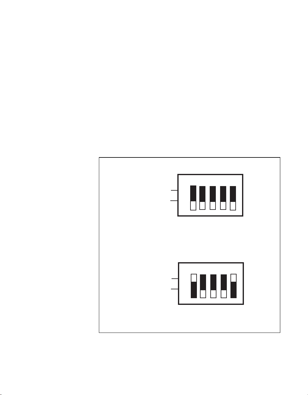
the other hardware base address to avoid a conflict. Figure 2-3 shows a
graphical representation of the b ase add ress se lection D IP switc h, a nd
also shows how to reconfigure the selected base address.
Switch up for 1
Switch down for 0
Chapter 2 Configuration and Installation
U112
12345
O
N
O
F
F
A7
A9
A8
A6
A5
A. Switches Set to Base I/O Address of Hex 000
U112
12345
Switch up for 1
Switch down for 0
O
N
O
F
F
A9
A8
A7
A6
A5
B. Switches Set to Base I/O Address of Hex 220 (Factory Setting)
Figure 2-3.
©
National Instruments Corporation 2-3 AT-MIO-16X User Manual
Example Base I/O Address Switch Settings
Page 26
Chapter 2 Configuration and Installation
The base address DIP switch is arranged so that a logical 1 or true state
for the associated address selection bit is selected by pushing the toggle
switch up, or toward the top of the board. A lternate ly, a logical 0 or
false state is selected by pushing the toggle switch down, or toward the
bottom of the board. In Figur e 2-3B, A 9 is up (tr ue), A8 thro ugh A6
are low (false), and A5 is up (true). This repres ents a binary value of
10001XXXXX, or hex 220. The Xs indicate don’t care bits and are the
five least significant bits (LSBs) of the a ddre ss (A 4 throu gh A0 ) use d
by the AT-MIO-16X circuitry to decode the individual register
selections. The don’t care bits indicate the size of the register space. In
this case, the AT-MIO-16X u ses I/O a ddress he x 2 20 th rough h ex 23 F
in the factory-default setting.
Note: If you change the AT-MIO-16X base I/O addres s, yo u must make a
corresponding change to any so ftware pac kage s you use with the
AT-MIO-16X. Table 2-1 lists the default settings of other National
Instruments products for the PC. Table 2-2 lists the possible switch
settings, the corresponding base I/O address, and the base I/O address
space used for that setting. For more information about the I/O address
of your PC, refer to the technical reference manual for your computer.
Table 2-1. Default Settings of National Instruments Products for the PC
Board DMA
AT-A2150 None* None* 120 hex
AT-AO-6/10 Channel 5 Lines 11, 12 1C0 hex
AT-DIO-32F Channels 5, 6 Lines 11, 12 240 hex
AT-DSP2200 None* None* 120 hex
AT-GPIB Channel 5 Line 11 2C0 hex
AT-MIO-16 Channels 6, 7 Line 10 220 hex
AT-MIO-16D Channels 6, 7 Lines 5, 10 220 hex
AT-MIO-16F-5 Channels 6, 7 Line 10 220 hex
AT-MIO-16X None* None* 220 hex
AT-MIO-16X User Manual 2-4
Channel
Interrupt
Level
©
National Instruments Corporation
Base I/O
Address
Page 27
Chapter 2 Configuration and Installation
Table 2-1. Default Settings of National Instruments Products for the PC (Continued)
Board DMA
Channel
Interrupt
Level
Base I/O
Address
AT-MIO-64F-5 None* None* 220 hex
GPIB-PCII Channel 1 Line 7 2B8 hex
GPIB-PCIIA Channel 1 Line 7 02E1 hex
GPIB-PCIII Channel 1 Line 7 280 hex
Lab-PC Channel 3 Line 5 260 hex
PC-DIO-24 None Line 5 210 hex
PC-DIO-96 None Line 5 180 hex
PC-LPM-16 None Line 5 260 hex
PC-TIO-10 None Line 5 1A0 hex
* These settings are software configurable and are disabled a t sta rt up ti m e.
Table 2-2. Switch Settings with Corresponding Base I/O Address and
Base I/O Address Space
Switch Setting
A9 A8 A7 A6 A5
Base I/O
Address (hex)
Base I/O
Address Space
Used (hex)
0 0 X X X 000 - E00 Reserved
0 1 0 0 0 100 100 - 11F
0 1 0 0 1 120 120 - 13F
0 1 0 1 0 140 140 - 15F
0 1 0 1 1 160 160 - 17F
0 1 1 0 0 180 180 - 19F
0 1 1 0 1 1A0 1A0 - 1BF
©
National Instruments Corporation 2-5 AT-MIO-16X User Manual
Page 28

Chapter 2 Configuration and Installation
Table 2-2. Switch Settings with Corresponding Base I/O Address and
Base I/O Address Space (Continued)
Switch Setting
A9 A8 A7 A6 A5
Base I/O
Address (hex)
Base I/O
Address Space
Used (hex)
0 1 1 1 0 1C0 1C0 - 1DF
0 1 1 1 1 1E0 1E0 - 1FF
1 0 0 0 0 200 200 - 21F
1 0 0 0 1 220 220 - 23F
1 0 0 1 0 240 240 - 25F
1 0 0 1 1 260 260 - 27F
1 0 1 0 0 280 280 - 29F
1 0 1 0 1 2A0 2A0 - 2BF
1 0 1 1 0 2C0 2C0 - 2DF
1 0 1 1 1 2E0 2E0 - 2FF
1 1 0 0 0 300 300 - 31F
1 1 0 0 1 320 320 - 33F
1 1 0 1 0 340 340 - 35F
1 1 0 1 1 360 360 - 37F
1 1 1 0 0 380 380 - 39F
1 1 1 0 1 3A0 3A0 - 3BF
1 1 1 1 0 3C0 3C0 - 3DF
1 1 1 1 1 3E0 3E0 - 3FF
AT-MIO-16X User Manual 2-6
©
National Instruments Corporation
Page 29

Interrupt and DMA Channel Selection
The base I/O address selection is the only resource on the AT-MIO-16X
board that must be set manually before the board is placed into the PC.
The interrupt level and DMA channels used by the AT-MIO-16X are
selected via registers in the AT-MIO-16X register set. The
AT-MIO-16X powers up with all interrupt and DMA requests disabled.
To use the interrupt capability of the AT-MIO-16X, an interrupt level
must first be selected via register programming, then the specific
interrupt mode must be enabled. The same method holds for DMA
channel selection. To use the DMA capability of the board, one or two
DMA channels must be selected through the appropriate register, then
the specific DMA mode must be enabled. It is possible to have interrupt
and DMA resourc es con cur rently en ab led.
The interrupt lines supported by the AT-MIO-16X hardware are IRQ3,
IRQ4, IRQ5, IRQ7, IRQ10, IRQ11, IRQ12, and IRQ15. The DMA
channels supported are Channe ls 0 through 3, and Channe ls 5
through 7. If you use the AT-MIO-16X in an AT-ty pe compute r, you
should only use DMA Channels 5 through 7 beca use these are the only
16-bit channels available. If you use the board in an EISA computer, all
channels are capable of 16- bit transfers an d you can use them . The
AT-MIO-16X does not use and cannot be configured to use th e 8-b it
DMA Channels 0 throug h 3 o n the PC I /O chan ne l fo r 16-bit tra nsf ers.
Chapter 2 Configuration and Installation
Analog Input Configuration
The analog input section of the AT-MIO-16X is software configurable.
You can select different analog in put config urations by progr amming
the appropriate register in the AT-MIO-16X register set. The following
paragraphs describe in detail each of the analog input categories.
Input Mode
The AT-MIO-16X offer s th ree diff er ent inpu t m odesSE) inp ut,
referenced single-en de d (RSE ) in put, and diff eren tial (DI FF) input.
The single-ended input conf igura tions use u p to 16 cha nnels. T he
DIFF input configuration uses up to eight channels. Input modes are
programmed on a per chann el basis for multimode scanning. For
example, the circuitry can be conf igured to effectively sca n
12 channels, four diffe rentia lly c onfigur ed cha nne ls and ei ght
single-ended channels. The in put configura tions are de scribe d in
Table 2-3.
©
National Instruments Corporation 2-7 AT-MIO-16X User Manual
Page 30
Chapter 2 Configuration and Installation
Table 2-3.
Available Input Configurations for the AT-MIO-16X
Configuration Description
DIFF Differential configurationnput of the PGIA tied to
the multiplexer output of Channels 8 thro ugh 15.
RSE Referenced single-end ed configurationve ( –) input
of the PGIA referenced to analog ground.
NRSE Nonreferenced single-ended configurationative (–)
input of the PGIA tied to AI SENSE and not
connected to ground.
While reading the following paragraphs, you may find it helpful to refer
to the Analog Input Signal Connections section later in this chapter,
which contains diagrams showing the signal paths for the three
configurations.
DIFF Input (Eight Channels)
DIFF input means that each input signal has its own reference, an d the
difference bet ween each sign al and its re ference is me asured. The signa l
and its reference are assigned an input channel. This is the
recommended con figura tion. With this inpu t c onfigur ation , th e
AT-MIO-16X can monitor up to eigh t different ana log input signals.
This configuration is se lect ed v ia softwa re. See th e co nfig uration
memory register a nd T abl e 4-9 i n Cha pt er 4, Register Map and
Descriptions. The results of this configuration are as follows:
• One of Channels 0 thro ugh 7 is tied to the p ositive (+) inpu t of
the PGIA.
• One of Channe ls 8 thro ugh 15 is tied to the neg ative (–) inp ut o f
the PGIA.
• Multiplexer control is configured to control up to eight input
channels.
• AI SENSE may be driven by the board analog input ground or left
unconnected.
Considerations for using the DIFF input configuration are discussed in
the Signal Connections section later in this chapter. Figure 2-8 shows a
schematic diagram of this configuration.
AT-MIO-16X User Manual 2-8
©
National Instruments Corporation
Page 31

Chapter 2 Configuration and Installation
RSE Input (16 Channels)
RSE input means that all input signals are referenced to a common
ground point that is also tied to the analo g in put gro und of the
AT-MIO-16X board. Th e negative (–) input of the differ ential input
amplifier is tied to the analog ground. This configuration is useful when
measuring flo ati ng sign al sour ces . Se e t he Type s of Sign al So urces
section later in this chapter for more information. With this input
configuration, the AT-MIO- 16X ca n mo nitor up to 16 differ e nt analog
input signals. This configuration is selected via softw are. See th e
configuration memory re gister a nd Tab le 4-9 in Cha pter 4, Register
Map and Descriptions. The resu lt s of th is con figu ra t io n ar e as fo llow s:
• The negative (–) input of the PGIA is tied to the PGIA signal
ground.
• Multiplexer outputs are tied together into the positive (+) input
of the PGIA.
• Multiplexer control is configur ed to control up to 16 input
channels.
• AI SENSE may be dr iven b y the board a nal og inpu t groun d o r
left unconnected.
Considerations for using the R SE co nfigura tion are disc ussed in the
Signal Connections section later in this chapter. Figure 2-18 shows
a schematic diagram of this configuration.
NRSE Input (16 Channels)
NRSE input means that all input signals are referenced to the same
common-mode voltage, but this com mon-mode voltage can floa t
with respect to the analo g g round of the A T-M IO-1 6X b oard. This
common-mode voltage is subsequently subt racted from the signals
by the input PGIA. This configuration is useful when measuring
ground-referenced signal sources. See the Types of Signal Sources
section later in this chapter for more information. With this input
configuration, the AT-MIO-16X can measure up to 16 different analog
input signals. This configuration is selected via softw are. See th e
configuration memory re gister a nd Tab le 4-9 in Cha pter 4, Register
Map and Descriptions, for additional information. The results of this
configuration ar e as fol lows:
• AI SENSE is tied into the negative (–) input of the PGIA.
• Multiplexer outputs are tied together into the positive (+) input
of the PGIA.
©
National Instruments Corporation 2-9 AT-MIO-16X User Manual
Page 32

Chapter 2 Configuration and Installation
• Multiplexer control is configur ed to control up to 16 input
channels.
Note: The NRSE input mode is the only mode in which the AI SENSE signa l
from the I/O connector is used as an input. In all other modes, AI SENSE
is either programmed to be unused or driven with the board analog input
ground.
Considerations for using the NRSE input configuration are discussed in
the Signal Connections section later in this chapter. Figure 2-8 shows a
schematic diagram of this configuration.
Input Polarity and Input Range
The AT-MIO-16X has two polarities: unipolar in put and bipolar input.
Unipolar input means that the input voltage range is between 0 and V
where V
input voltage range is between –V
a maximum unipolar input range of 10 V, and a maximum bipolar input
range of 20 V (±10 V). Polarity and range settings are programmed on
a per channel basis through the co nfiguration me mory registe r.
is a positive reference voltage. Bipolar input means that the
ref
and +V
ref
. The AT-MIO-16X has
ref
ref
Considerations for Selecting Input Ranges
Input polarity and range selection depend on the expected input range
of the incoming signal. A large input range can accommodate a large
signal variation but lowers the voltage resolution. Choosing a smaller
input range increases the voltage resolution but may re sult in the input
signal going out of range. For best results, the input range should be
matched as closely as possible to the expected range of the input signal.
For example, if the input signal is certain not to be negative (below
0 V), a unipolar input is best. However, if the signal is ever negative,
inaccurate readings will occur if unipolar input polarity is used.
The software-p rog ramm able g ain on the AT -M IO-1 6X i n crea se s its
overall flexibility by matching the input signal ranges to those that the
AT-MIO-16X analog-to- digital converte r (ADC) can a ccommod ate.
The AT-MIO-16X board has gains of 1, 2, 5, 10, 20, 50, and 100 and is
suited for a wide variety of signal levels. With the proper gain setting,
the full resolution of the ADC can be used to measure the input signal.
Table 2-4 shows the overall input range and prec ision acco rding to the
input range configuration and gain used.
AT-MIO-16X User Manual 2-10
©
National Instruments Corporation
Page 33

Chapter 2 Configuration and Installation
Table 2-4.
Range
Configuration
0 to +10 V 1.0
–10 to +10 V 1.0
* The value of 1 LSB of the 16-bit ADC; that is, the voltage increment corresponding to
a change of 1 count in the ADC 16-bit count.
Note:
Actual Range and Measurement Precision Versus Input Range
Selection and Gain
Gain Actual
Input Range
0 to +10.0 V
2.0
5.0
10.0
20.0
50.0
100.0
0 to +5.0 V
0 to +2.0 V
0 to +1.0 V
0 to +0.5 V
0 to +0.2 V
0 to 100.0 mV
–10.0 to +10.0 V
See Appendix A,
2.0
5.0
10.0
20.0
50.0
100.0
Specifications
–5.0 to +5.0 V
–2.0 to +2.0 V
–1.0 to +1.0 V
–0.5 to +0.5 V
–0.2 to +0.2 V
–100.0 to +100.0 mV
, for absolute maximum rati ngs.
Precision*
152.59 µV
76.29 µV
30.52 µV
15.26 µV
7.63 µV
3.05 µV
1.53 µV
305.18 µV
152.59 µV
61.04 µV
30.52 µV
15.26 µV
6.10 µV
3.05 µV
Analog Output Configuration
The AT-MIO-16X supplies two c hannels of anal og output voltag e at
the I/O connector. The analog output circuitry is configurable through
programming of a register in th e board reg ister se t. The refer ence an d
range for the analog o utput ci rcuitry ca n be selecte d thr ough sof tw are.
The reference can be either internal or external, whereas the range can
be either bipolar o r unipolar .
Analog Output Reference Selection
Each DAC can be connected to the AT-MIO-16X internal reference of
10 V or to the external reference signal connected to the EXTREF pin
on the I/O connector. This signal applied to EXTREF must be between
–18 and +18 V. Both channels ne ed not be configu red for the same
mode.
©
National Instruments Corporation 2-11 AT-MIO-16X User Manual
Page 34

Chapter 2 Configuration and Installation
Analog Output Polarity Selection
Each analog output c ha nnel c an be c onf igur ed fo r eithe r unipo lar or
bipolar output. A unipolar configuratio n has a range of 0 to V
analog output. A bi polar con figura tion h as a ra ng e of –V
the analog output. V
analog output circuitry and can be either the 10-V onboard reference or
an externally supplied reference between –18 and +18 V. Both channels
need not be configu red f or the sa m e ra nge.
Selecting a bipolar range for a particular DAC means that any data
written to that DAC will be interpreted as two’s complement format.
In two’s complement mode, data values written to the analog output
channel range from –32,768 to +32,767 decimal (8000 to 7FFF hex). If
unipolar range is selected, data is interpr eted in straight bina ry forma t.
In straight binary mode, data values written to the analog output channel
range from 0 to 65,535 decimal (0 to FFFF hex).
Digital I/O Configuration
The AT-MIO-16X contain s eight lines of digital I/O for
general-purpose use. The eight digital I/O lines supplied are configured
as two 4-bit ports. Each po rt can b e individua lly conf igur ed thr ough
programming of a r egis ter in th e boa rd reg is ter se t a s ei ther inp ut or
output. At system startup and reset, the digital I/O ports are both
configured for input.
at the
ref
to +V
is the voltage reference used by t he DACs i n the
ref
ref
ref
at
Board and RTSI Clock Configuration
When multiple AT Series boards are connected via the RTSI bus,
you may want all of the boa rds to use the same 10-MH z c lock. T his
arrangement is useful for applications that require counter/timer
synchronization between boards. Each AT Series board with a RTSI bus
interface has an onboard 10-MHz oscillator. Thus, one board can drive
the RTSI bus clock signal, and the other b oards c an r eceive this signa l
or disconnect from it.
Many functions pe rfo rmed by the AT -M IO- 16X boa rd requ ir e a
frequency timebase to generate the necessary timing signals for
controlling ADC conversions, DAC updates, or general-purpose signals
at the I/O connector. You select this t imebase through programming one
of the registers in the AT-MIO-16X register set.
AT-MIO-16X User Manual 2-12
©
National Instruments Corporation
Page 35

The AT-MIO-16X can use either its internal 10-MHz timebase, or it can
use a timebase received over the RTSI bus. In addition, if the board is
configured to use the internal timebase, it can also be programmed to
drive its internal timebase over the RTSI bus to another board that is
programmed to re ceive this timeb ase signal. Th is clock sourc e, whether
local or from the RTSI bus, is then divided by 10 and used as the
Am9513A frequency source. The defau lt config uration at startup is to
use the internal timebase without driving the RTSI bus timebase signal.
Hardware Installation
You can install the AT-MIO-16X in any avai lable 16-bit ex pansion
slot in your AT Series computer. However, to achieve best noise
performance, yo u should leave as muc h room a s possible betwee n the
AT-MIO-16X and other boa rds and har dw are . Th e AT -MIO -1 6X does
not work if installed in an 8 -b it ex pansion slot (P C Serie s). A fter yo u
have made any necessary chan ges, verifie d, and reco rded the switch es
and jumper settings (a form is included for this purpose in Appendix D,
Customer Communication), you are ready to install the AT-MIO-16X.
The following are general installation instructions, but consult your PC
user manual or technical reference manual for specific instructions and
warnings.
1. Tu rn off y our c ompute r.
2. Remove the top cover or access port to the I/O channel.
3. Remov e the expansion slot cove r on the back panel of the
computer.
4. Insert the AT-MIO-16X into a 16-bit slot. Do not force the board
into place. Verify that there are no extended components on the
circuit board of the co mpu ter tha t m ay touc h or be in the wa y of
any part of the AT-M IO- 16X .
5. Attach a RTSI cable to the RTSI connectors to connect AT Series
boards to each other.
6. Screw the AT-MIO-16X mounting bracket to the back panel rail
of the computer.
7. Check the installation.
8. Replace the cover.
Chapter 2 Configuration and Installation
The AT-MIO-16X board is installe d and re ady fo r o pera tion.
©
National Instruments Corporation 2-13 AT-MIO-16X User Manual
Page 36

Chapter 2 Configuration and Installation
Signal Connections
This section describes input and output signal connections to the
AT-MIO-16X board via the AT-M IO-16X I/O connector . This section
also includes specifications and connection instructions for the signals
given on the AT-MIO-16X I/O connector .
Caution: Connections that exceed any of the maximum ratings of input or output
signals on the AT-MIO-16X can result in damage to the AT -MIO-16 X
board and to the PC. Maximum input ratings for each signal are given in
this chapter under the discussion of that signal. National Instruments is
not liable for any damages resulting from such signal connections.
AT-MIO-16X User Manual 2-14
©
National Instruments Corporation
Page 37

Chapter 2 Configuration and Installation
Figure 2-4 shows the pin assignments for the AT-MIO-16X 50-pin I/O
connector.
AI GND
ACH0
ACH1
ACH2
ACH3
ACH4
ACH5
ACH6
ACH7
AI SENSE
DAC1 OUT
AO GND
ADIO0
ADIO1
ADIO2
ADIO3
DIG GND
+5 V
EXTSTR OBE*
EXTGATE*
SOURCE1
OUT1
GATE2
SOURCE5
OUT5
1
2
43
65
87
109
1211
1413
1615
1817
2019
2221
2423
2625
2827
3029
3231
3433
3635
3837
4039
4241
4443
4645
4847
5049
AI GND
ACH8
ACH9
ACH10
ACH11
ACH12
ACH13
ACH14
ACH15
DAC0 OUT
EXTREF
DIG GND
BDIO0
BDIO1
BDIO2
BDIO3
+5 V
SCANCLK
EXTTRIG*
EXTCONV*
GATE1
EXTTMRTRIG*
OUT2
GATE5
FOUT
Figure 2-4. AT-MIO-16X 50-Pin I/O Connector
©
National Instruments Corporation 2-15 AT-MIO-16X User Manual
Page 38

Chapter 2 Configuration and Installation
Figure 2-5 shows the pin assignments for the AT-MIO-16X 68-pin I/O
connector.
ACH8
ACH1
AIGND
ACH10
ACH3
AIGND
ACH4
AIGND
ACH13
ACH6
AIGND
ACH15
DAC0
DAC1
EXTREF
BDIO0
DGND
ADIO1
BDIO2
DGND
+5 V
DGND
DGND
EXTTRIG*
EXTGATE*
DGND
+5 V
DGND
EXTTMRTRIG*
GATE2
DGND
GATE5
OUT5
FOUT
34
68
ACH0
67
66
65
64
63
62
61
60
59
58
57
56
55
54
5319
52
51
50
49
48
47
46
45
44
43
42
41
40
39
38
37
36
35
AIGND
ACH9
ACH2
AIGND
ACH11
AISENSE
ACH12
ACH5
AIGND
ACH14
ACH7
AIGND
AOGND
AOGND
DGND
ADIO0
BDIO1
DGND
ADIO2
BDIO3
ADIO3
SCANCLK
EXTSTROBE*
DGND
EXTCONV*
SOURCE1
GATE1
OUT1
DGND
OUT2
SOURCE5
DGND
DGND
33
32
31
30
29
28
27
26
25
24
23
22
21
20
18
17
16
15
14
13
12
11
10
9
8
7
6
5
4
3
2
1
Figure 2-5. AT-MIO-16X 68-Pin I/O Connector
AT-MIO-16X User Manual 2-16
©
National Instruments Corporation
Page 39

Chapter 2 Configuration and Installation
Signal Connection Descriptions
Signal Names Reference Descriptions
AI GND N/A Analog Input Ground—These pins are the refer ence point for
single-ended measurements and the bias current return point
for differential measurements.
ACH<0..15> AI GND Analog Input Channels 0 through 15—In differential mode,
the input is configured for up to eight channels. In
single-ended mode, the input is configured for up to
16 channels.
AI SENSE AI GND Analog Input Sense—This pin serves as the reference node
when the board is in NRSE configuration. If desired, this
signal can be programmed to be driven by the board analog
input ground in the DIFF and RSE analog input modes.
DAC0 OUT AO GND Analog Channel 0 Output—Thi s pin supplies the voltage
output of analog output Channel 0.
DAC1 OUT AO GND Analog Channel 1 Output—Thi s pin supplies the voltage
output of analog output Channel 1.
EXTREF AO GND External Reference—This is the external reference input for
the analog output circuitry.
AO GND N/A Analog Output Ground—The analog output voltages are
referenced to this node.
DIG GND N/A Digital Ground—This pin supplies the reference for the
digital signals at the I/O connector as well as the +5 VDC
supply.
ADIO<0..3> DIG GND Digital I/O port A signals.
BDIO<0..3> DIG GND Digita l I/ O port B si gna l s .
+5 V DIG GND +5 VDC Source—These pins are fused for up to 1 A of +5 V
supply.
©
National Instruments Corporation 2-17 AT-MIO-16X User Manual
Page 40

Chapter 2 Configuration and Installation
Signal Names Reference Descriptions
SCANCLK DIG GND Scan Clock—This pin pulses once for each A/D conversion in
the scanning modes. The low-to-high edge indicates when the
input signal can be removed from the input or switched to
another signal.
EXTSTROBE* DIG GND External Strobe—Writing to the EXTSTROBE Register
results in a minimum 500-nsec low pulse on this pin.
EXTTRIG* DIG GND External Trigger—In posttrigger data acquisition sequences, a
high-to-low edge on EXTTRIG* initiates the sequence. In
pretrigger applications, the first high-to-low edge of
EXTTRIG* initiates pretrigger conversions while the second
high-to-low edge initiates the posttrigger sequence.
EXTGATE* DIG GND External Gate—When EXTGATE* is low, A/D conversions
are inhibited. When EXTGATE* is high, A/D conversions are
enabled.
EXTCONV* DIG GND External Convert—A high-to-low edge on EXTCONV*
causes an A/D conversion to occur. Conversions initiated by
the EXTCONV* signal are inhibited outside of a data
acquisition sequence, and when gated off.
SOURCE1 DIG GND SOURCE1—This pin is from the Am9513A C ounter 1 si gnal.
GATE1 DIG GND GATE1—This pin is from the Am9513A Counter 1 signal.
OUT1 DIG GND OUTPUT1—This pin is from the Am9513A Coun ter 1 signal.
EXTTMRTRIG* DIG GND External Timer Trigger—If selected, a high-to-low edge on
EXTTMRTRIG* results in the output DACs being updated
with the value written to them in the posted update mode.
EXTTMRTRIG* will also generate a timed interrupt if
enabled.
GATE2 DIG GND GATE2—This pin is from the Am9513A Counter 2 signal.
OUT2 DIG GND OUTPUT2—This pin is from the Am9513A Coun ter 2 signal.
SOURCE5 DIG GND SOURCE5—This pin is from the Am9513A C ounter 5 si gnal.
GATE5 DIG GND GATE5—This pin is from the Am9513A Counter 5 signal.
©
AT-MIO-16X User Manual 2-18
National Instruments Corporation
Page 41

Chapter 2 Configuration and Installation
Signal Names Reference Descriptions
OUT5 DIG GND OUT5—This pin is from the Am9513A Counter 5 signal.
FOUT DIG GND Frequency Output—This pin is from the Am9513A FOUT
signal.
The signals on the connector can be classified as analog input signals,
analog output signals, digital I/O signals, digital power connections, or
timing I/O sign al s. Si gnal co nnec tion g ui de lin es fo r e ach o f t hes e
groups are given in the following section.
Analog Input Signal Connections
AI GND is an analog input common signal that is routed directly to
the ground tie point on the AT-MIO-16X. These pins can be used for a
general analog power ground tie point to the AT-MIO-16X if necessary.
In NRSE mode, AI SENSE is connected internally to the negative (–)
input of the AT-MIO-1 6X PG IA. In th e DIFF a nd RSE m odes, this
signal is driven by AI GND or left unconnected.
Signal pins ACH<0..15> are tied to the 16 analog input channels of
the AT-MIO-16X. In single -ende d mode, s igna ls c onn ected to
ACH<0..15> are routed to the positive (+) input of the AT-MIO-16X
PGIA. In differential mode, signals connected to ACH<0..7> are r outed
to the positive (+) input of the AT-MIO-16X PGIA, and signals
connected to ACH<8..15> are routed to the negative (–) input of the
AT-MIO-16X PGIA.
Caution: Exceeding the differential and common-mode input ranges results in
distorted input signals. Exceeding the maximum input voltage r ating can
result in damage to the AT-MIO-16X board and to the PC. National
Instruments is not liable for any damages resulting from such signal
connections.
Connection of analog input signals to the AT-MIO-16X depends on the
configuration of the AT-MIO-16X ana log input circuitry and the type
of input signal source. With the different AT-MIO-16X configurations,
you can use the AT- MIO-16 X PG IA in dif ferent wa ys. Figu re 2-6
shows a diagram of the A T-M IO- 16X PG I A.
©
National Instruments Corporation 2-19 AT-MIO-16X User Manual
Page 42

Chapter 2 Configuration and Installation
+
V
in
Programmable Gain
+
-
V
in
-
Gain = 1, 2, 5, 10, 20, 50, 100
=
V
m
The AT-MIO-16X PGIA applie s gain and comm on-mode volta ge
rejection, and presents high-input impedance to the analog input signals
connected to the AT-MIO-16X board. Signals are routed to the positive
(+) and negative (–) inputs of the PGIA through input multiplexers on
the AT-MIO-16X. The PG IA co nver ts two i nput sig nals to a si gnal that
is the difference between the two input signals multiplied by the gain
setting of the amplifier. The amplifier output voltage is referenced to
the AT-MIO-16X groun d. The AT- MIO-16 X ADC mea sures this
output voltage when it perf orms A/D co nve rsions.
Gain
+
[
V
in
Figure 2-6. AT-MIO-16X PGIA
-
]
V
-
in
*
GAIN
V
m
+
Measured
Voltage
-
All signals must be referenced to ground, either at the source device or
at the AT-MIO-16X. If you have a floating source, the AT-MIO -16X
should reference the signa l to groun d b y using the RSE inp ut m ode or
the DIFF input configuration with bias resistors (see the Dif fe r en tia l
Connections for Nonreferenced or Floating Signal Sources section later
in this chapter). If y ou have a g rou nded sour ce, the AT -MIO -1 6X
should not reference the signal to AI GND. The AT-MIO-16X board
avoids this reference by using the DIFF or NRSE input configurations.
AT-MIO-16X User Manual 2-20
©
National Instruments Corporation
Page 43

Types of Signal Sources
When configuring the input mode of the AT-M IO-16X and making
signal connections, you must first determine whether the signal source
is floating or ground-re fere nced . Thes e tw o type s o f signa ls a re
described in the following sec tions.
Floating Signal Sources
A floating signal source is one that is not connected in any way to the
building ground system but r a ther has an isolat ed gr oun d refe renc e
point. Some examples of floating signal sources are outputs of
transformers, thermocouples, battery-powered devices, optical isolator
outputs, and isolation amplifiers. An instrument or device that provides
an isolated output falls into the floa ting signa l so urce categor y. T he
ground reference of a f loa ting sign al m ust be tied to the AT -MIO -1 6X
analog input ground in order to establish a local or onboa rd refere nce
for the signal. Otherwise, the measured input signal varies as the source
floats out of the comm on- mod e inpu t ra ng e.
Ground-Referenced Signal Sources
A ground-referenced signal source is one that is connected in some way
to the building system ground and is therefore alr eady conne cted to a
common ground po int with r espe ct to the A T-M IO -16X b oard,
assuming that the PC AT is plugged into the same power system.
Nonisolated outputs of instrume nts and devices that plug into the
building power system fall into this category.
Chapter 2 Configuration and Installation
The difference in ground potential betw een two instruments connected
to the same building pow er sy stem is ty pically be twee n 1 m V a nd
100 mV but can be much higher if power distribution circuits are not
properly connected. If grounded signal source is improperly measured,
this difference may show up as an error in the measurement. The
following connection instructions for ground ed signal source s are
designed to eliminate this g rou nd potential diff eren ce fro m th e
measured signal.
Input Configurations
The AT-MIO-16X can be con figured for one of three input modes:
NRSE, RSE, or DIFF. The following sections discuss the use of
single-ended and diff er en tial mea sur em ents, an d c on sider ation s f or
measuring both fl oatin g a nd groun d-r e fere nced sign al sour ces.
©
National Instruments Corporation 2-21 AT-MIO-16X User Manual
Page 44

Chapter 2 Configuration and Installation
Table 2-5 summarizes the recommended input co nfiguration for both
types of signal sources.
Table 2-5.
Recommended Input Configurations for Ground-Referenced and
Floating Signal Sources
Type of Signal Recommended Input
Configuration
Ground-referenced (nonisolated outputs,
plug-in instruments)
Floating (batteries, thermocouples, isolated
outputs)
DIFF
NRSE
DIFF with bias re sistors
RSE
Differential Connection Considerations
(DIFF Input Configuration)
Differential connections are those in which each AT-MIO-16X analog
input signal has its own reference signal or signal return path. These
connections are available when the AT-MIO-16X is configured in the
DIFF input mode. Each input signal is tied to the positive (+) input of
the PGIA; and its reference signal, or return, is tied to the negative (–)
input of the PGIA.
When the AT-MIO- 16X is c onfigur ed for differ ential in put, each sig nal
uses two multiplexer inputs—one for the signal and one for its re ference
signal. Therefore, with a differential configuration, up to eight analog
input channels are available. Differential input conn ections shou ld be
used when any of the following conditions are presen t:
• You are connectin g eight or few er signa ls to the AT-MI O-16X.
• Input signals are low level (less than 1 V).
• Leads connecting the signals to the AT-MIO-16X are greater than
10 ft.
• Any of the input signals require a se para te ground -re fere nce po int
or return signal.
• The signal leads travel through noisy environments.
Differential signal connections reduce picked-up no ise an d increase
common-mode noise rejection. Di fferential signal con nections also
permit input signals to float within the common-mode limits of the
PGIA.
AT-MIO-16X User Manual 2-22
©
National Instruments Corporation
Page 45

Chapter 2 Configuration and Installation
R
Differential Connections for Ground-Referenced
Signal Sources
Figure 2-7 shows how to co nnec t a gr ound-r efe renc ed sign al s ource
to an AT-MIO-16X board configured in the DIFF input mode. The
AT-MIO-16X analog input circuitry must be configured for DIFF input
to make these types of connections. Configuration instructions are
included in Chapter 4, Register Map and Descriptions.
ACH<0..7>
Ground-
eferenced
Signal
Source
CommonMode
Noise,
Ground
Potential,
and so on
+
V
s
-
ACH<8..15>
+
V
cm
-
Input Multiplexers
+
-
Gain
PGIA
V
m
+
Measured
Voltage
-
AI SENSE
AI GND
I/O Connector
AT-MIO-16X Board in the DIFF Input Configuration
Figure 2-7.
Differential Input Connections for Ground-Referenced Signals
With this type of connection, the PGIA rejects both the common-mode
noise in the signal and the ground potential difference betwee n the
signal source and the AT- MIO -16X groun d, shown as V
cm
in
Figure 2-7.
©
National Instruments Corporation 2-23 AT-MIO-16X User Manual
Page 46

Chapter 2 Configuration and Installation
F
S
S
Differential Connections for Nonreferenced or
Floating Signal Sources
Figure 2-8 shows how to conne ct a flo ating sign al s ource to an
AT-MIO-16X board configur ed in the DIFF input mode. The
AT-MIO-16X analog input circ uitry must be configu red for DIFF
input to make these types of connections. Configuration instructions are
included in Chapter 4, Register Map and Descriptions.
Bias
Resistors
loating
ignal
ource
+
V
s
-
ACH<0..7>
PGIA
+
ACH<8..15>
Bias
Current
Return
Paths
Input Multiplexers
AI SENSE
I/O Connector
AI GND
AT-MIO-16X Board in the DIFF Input Configuration
Figure 2-8.
Differential Input Connections for Nonreferenced Signals
Gain
-
+
Measured
V
m
Voltage
-
Figure 2-8 shows two bias resistors connected in parallel with the signal
leads of a floating signal source. If the source is truly floating, it is not
likely to remain within the common-mode signal range of the PGIA,
and the PGIA will saturate (causing erro neous read ings). You must
reference the source to AI GND. The best way is simply to connect the
positive side of the signal to the positive (+) input of the PGIA and
AT-MIO-16X User Manual 2-24
©
National Instruments Corporation
Page 47

Chapter 2 Configuration and Installation
connect the negative side of the signal to AI GND as well as to the
negative (–) input of the PGIA. This works well for DC-coupled sources
with low source impedance (less than 100 Ω). How eve r, for la rger
source impedances, this connectio n leaves the differentia l signal path
significantly out of balance. Noise that couples electrostatically onto
the positive (+) line does not couple onto the ne gative (–) line because
it is connected to ground. Hence, this noise appears as a
differential-mode signal instead of a common-mode signal, and so the
PGIA does not reject it. In this case, instead of directly connecting the
negative (–) line to AI GND, connect it to AI GND through a resistor
that is about 100 times the equivalent source impedance . This puts the
signal path nearly in balance, so about the same noise couples onto both
(+) and (–) connections, yielding better rejection of electrostatically
coupled noise. Also, this configuration does not load down th e source
(other than the 100-GΩ input impedance of the PGIA). You can fully
balance the signal path by connecting another resistor of the same value
between the positive (+) input and AI GND. This fully balanced
configuration offers slightly better noise rejection, but has the
disadvantage of loading the source down with the series combination
(sum) of the two resistors. If, for instance, the source impedance is 2 kΩ
and the two resistors are ea ch 10 0 kΩ, the resistors load down the
source with 200 kΩ and produc e a –1% gain erro r.
Both inputs of the PGI A re quir e a DC pa th to gr ound in or der f or the
PGIA to work. If the source is AC coupled (capacitively coupled), then
the PGIA needs a resistor between the positive (+) input and AI GND.
If the source has low impedance, choose a resis tor that is large enough
not to significantly load the source, but small enough not to produce
significant input offset voltage as a result of input bias current (typically
100 kΩ to 1 MΩ). If the source has high output impedance, you should
balance the signal path (as described above) using the same value
resistor on both the positive (+) and negative (–) inputs, and you should
be aware that there is some gain error from loading down the source.
The PGIA obtains its input DC bias currents from the DC paths to
ground. These currents are typically less than ±1 nA, but they contribute
significantly to erro r wh en ev er t he so ur ce has mo re t ha n 1 kΩ
impedance or is AC coupled. If the source is DC coupled, the resulting
DC offset is less than 1 nA times the DC source resistance. For instance,
a 1-kΩ source will produce no more than 1 µV of input offset (0.33 LSB
at a gain of 100, bipolar range). If the sou rce is AC couple d, then the
resulting DC offset is less than 1 nA times the sum of the two bias
©
National Instruments Corporation 2-25 AT-MIO-16X User Manual
Page 48

Chapter 2 Configuration and Installation
resistors. For example, if tw o 1 00-k Ω bias resistors are used, there
could be as much as 200 µV of input offset voltag e ( 0. 6 6 L SB at a g ai n
of 1, bipolar range).
Single-Ended Connection Considerations
Single-ended connections are those in which all AT-MIO-16X analog
input signals are referenc ed to one com mon g round. T he inp ut signa ls
are tied to the positive (+) input of the PGIA, and their common ground
point is tied to the negative ( –) input of the PG IA.
When the AT-MIO-16X is configured for single-ended input, up to
16 analog input channels are available. Single-ended input connections
can be used when all input signals meet the following criteria:
• Input signals are high level (greater than 1 V).
• Leads connecting the signals to the AT-MIO-16X are less than
15 ft.
• All input signals share a common-re ferenc e signal (at the source )
or are floating.
DIFF input connectio ns are reco mmen ded fo r gr eater signal integ rity i f
any of the precedi ng crit eria ar e not met .
The AT-MIO-16X can be softw are-config ured for two diff erent
types of single-ended connections: RSE configura tion and NRSE
configuration. The RSE c onfigur ation is use d for floating signal
sources; in this case, the AT-MIO-16 X provides the refe rence ground
point for the external signal. The NRSE input configuration is used for
ground-referenced signal sources; in this case, the external signal
supplies its own refe renc e groun d p oint a nd the AT -M IO- 16X s hould
not supply one.
If using the AT-MIO-16X with a 50-pin I/O co nnec tor in single -ende d
configurations, more electrostatic and magnetic noise couples into the
signal connections than in dif ferential co nfigura tions. Mor eover , the
amount of coupling varies among channels, especially if a ribbon cable
is used. The coupling is the result of differences in the signal path.
Magnetic coupling is proportional to the area between the two signal
conductors. Electrical coupling is a function of how much the electric
field differs between the two conductors. If AI GND is used as the
signal reference, Channels 0 and 8 ar e the quiete st and Channe ls 7 and
15 are the noisiest. AI GND is on pins 1 and 2, which are very close to
pins 3 and 4, which are Channels 0 and 1. On the other hand, Channels 7
AT-MIO-16X User Manual 2-26
©
National Instruments Corporation
Page 49

Chapter 2 Configuration and Installation
and 15 are on pins 17 and 18, which are the farth est analog inputs
from AI GND. The sensitivities to noise of the other channels in the
middle are between those of C hannels 0 and 15 an d vary acc ordin g to
their distance fro m AI GND. If AI SENSE is used as a reference i nstead
of AI GND, the sensitivity to noise still varies among the channels,
but in this case according to their distance from AI SENSE, pin 19
(so Channel 15 is the least sensitive and Channel 0 is the most
sensitive).
Single-Ended Connections for Floating Signal
Sources (RSE Configuration)
Figure 2-9 shows how to conne ct a flo ating sign al s ource to an
AT-MIO-16X board conf igured f or single-e nded inpu t. T he
AT-MIO-16X analog input circu itry must be configured for R S E input
to make these types of connections. Configuration instructions are
included in Chapter 4, Register Map and Descriptions.
ACH<0..15>
Nonreferenced
or Floating
Signal
Source
©
National Instruments Corporation 2-27 AT-MIO-16X User Manual
+
V
s
-
I/O Connector
Figure 2-9.
Gain
PGIA
V
m
+
Measured
Voltage
-
+
Input Multiplexer
AI SENSE
AI GND
AT-MIO-16X Board in the RSE Input Configuration
Single-Ended Input Connections for Nonreferenced or Floating Signals
-
Page 50

Chapter 2 Configuration and Installation
Single-Ended Connections for Grounded Signal
Sources (NRSE Configuration)
If a grounded signa l sou rce is to be m eas ure d with a single-e nded
configuration, then the AT-MIO- 16X mus t be conf igured in the NRSE
input configuration. The signal is connected to the positive (+) input of
the AT-MIO-16X PGIA and the signal local ground reference is
connected to the negative (–) input of the AT-MIO-16X PGIA. The
ground point of the signa l sh ould the refore be con nected to the AI
SENSE pin. Any potential difference between the AT-MIO-16X ground
and the signal ground ap pe ars a s a com mo n-m ode signa l at both the
positive (+) and negative (–) inputs of the PGIA and this difference is
rejected by the amplifie r. On t he other ha nd, if the i nput circ uitry of the
AT-MIO-16X is referenced to ground, such as in the RSE input
configuration, this difference in ground potentials appears as an error in
the measured voltage.
Figure 2-10 shows how to conn ect a g rounde d signa l so urce to an
AT-MIO-16X board c onfigur ed f or non refe renc ed sing le-en de d inp ut.
The AT-MIO-16X analog input circuitry must be configured for NRSE
input configuration to make these types of signals. Configur ation
instructions are included in Chapter 4, Register Map and Descriptions.
ACH<0..15>
Ground-
Referenced
Signal
Source
Common-
Mode
Noise
AT-MIO-16X User Manual 2-28
+
V
s
-
+
V
cm
-
I/O Connector
AT-MIO-16X Board in the NRSE Input Configuration
Figure 2-10.
Input Multiplexer
AI SENSE
AI GND
Single-Ended Input Connections for Ground-Referenced Signals
+
-
PGIA
+
Measured
V
m
Voltage
-
©
National Instruments Corporation
Page 51

Chapter 2 Configuration and Installation
Common-Mode Signal Rejection Considerations
Figures 2-7 and 2-8, located earlier in this chapter, show connections
for signal sources that are already referenced to some ground point with
respect to the AT-MIO-16X. In these cases, the PGIA can reject any
voltage caused by g round pote ntial differ en ces be tween the s ig nal
source and the AT-MIO-16X . In addition, with diff erential input
connections, the PGIA ca n rejec t c ommon -m ode n oise pickup in the
leads connecting the signal sources to the AT-MIO-16X.
The common-mod e input rang e of the AT-MIO- 16X PGIA is defi ned as
the magnitude of th e greatest com mon-mode signa l that can be r ejected.
The PGIA can reje ct co mm on- mode signals a s long a s V+
are both in the rang e ±1 1 V. Thu s, the c omm on-mo de rang e for th e
AT-MIO-16X depends on the size of the differential input signal
= V+in – V–in). The exact formula for the allowed common-mode
(V
diff
input range is as follows:
V
cm-max
= ±(11 V – V
diff
/2)
With a differential voltage of 10 V, the maxim um possib le
common-mode voltage is ±6 V. The common-mode voltage is m easu r e
with respect to the AT-MIO-16X ground and can be calculated by th e
following form ula:
()
V
cm actual–
where V+
is the signal at the positive (+) input of the PGIA and –in is
in
V+inV–in+
-----------------------------------=
2
the signal at the negative (–) input of the PGIA. Both V+
measured with respect to AI GND.
and V– in
in
and V–in are
in
Analog Output Signal Connections
DAC0 OUT is the voltage outp ut signa l fo r ana log outp ut C hannel 0.
DAC1 OUT is the voltage outp ut signa l fo r ana log outp ut C hannel 1.
EXTREF is the external referenc e input for both an alog output
channels. Each anal og o utput cha nnel mu st be configu re d indiv idua lly
for external reference selection in order for the signal applied at the
external referenc e inpu t to be us ed by that cha nnel. A nalog outpu t
configuration instructions are in the Analog Outpu t Con figuration
section earlier in this chapter.
©
National Instruments Corporation 2-29 AT-MIO-16X User Manual
Page 52

Chapter 2 Configuration and Installation
The following ranges a nd ratin gs ap ply to the E XTR EF input:
Normal input voltage range ±10 V peak with respect to AO GND
Usable input voltage range ±18 V pea k with respec t to AO GND
Absolute maximum ratings ±30 V peak with respec t to AO GND
AO GND is the ground reference point for both analog output channels
and for the external reference signal.
Figure 2-11 shows how to m ak e an alog ou tput co nne ctions and the
external reference input conn ection to the AT-M IO-16X boa rd.
External
Reference
Signal
(Optional)
+
V
ref
Load
VOUT 0
EXTREF
DAC0 OUT
+
-
AO GND
Channel 0
-
VOUT 1
Load
+
Figure 2-11. Analog Output Connections
The external re fere nc e si gn al ca n b e e ith er a D C or an A C si gna l. T hi s
reference signal is multiplied by the DAC code to generate the output
voltage.
AT-MIO-16X User Manual 2-30
DAC1 OUT
Channel 1
Analog Output Channels
AT-MIO-16X Board
©
National Instruments Corporation
Page 53

Digital I/O Signal Connections
The digital lines ADIO<0..3> are connected to digital I/O port A. The
digital lines BDIO<0..3> are connect ed to digital I/O port B. DIG GND
is the digital ground pin for both digital I/O ports. Ports A and B can be
programmed individually to be inputs or ou tputs.
The following specifications and ratings apply to the digital I/O lines.
Absolute maximum voltage input rating 5.5 V with respect to
Digital input specifications (referenced to DIG GND):
input logic high voltage 2 V minimum
V
IH
V
input logic low voltage 0. 8 V maximum
IL
I
input current load,
IH
logic high input voltage 40 µA maximum
I
input current load,
IL
logic low input voltage –120 µA maximum
Digital output specifications (referenced to DIG GND):
V
output logic high voltage 2.4 V minim um
OH
V
output logic low voltage 0.5 V maximum
OL
I
output source current,
OH
logic high 2.6 mA maximum
I
output sink current, logic lo w 24 mA maximu m
OL
Chapter 2 Configuration and Installation
DIG GND
With these specifications, each digital output line can drive 11 standard
TTL loads and o ver 5 0 LS TT L l oa ds.
Figure 2-12 depicts signal connections for three typic al digital I/O
applications.
©
National Instruments Corporation 2-31 AT-MIO-16X User Manual
Page 54

Chapter 2 Configuration and Installation
+5 V
LED
Port A
ADIO<3..0>
+5 V
Switch
Power Connections
TTL Signal
DIG GND
I/O Connector
Figure 2-12. Digital I/O Connections
Port B
BDIO<3..0>
AT-MIO-16X Board
In Figure 2-12, port A is configured for digital output, an d port B is
configured for digital input. Digital input applications include receiving
TTL signals and sensing external device states such as the state of the
switch in Figure 2-12. Digital output applications include sending TTL
signals and driving external devices such as the LED shown in
Figure 2-12.
The I/O connector provides +5 V from the PC power supply. This +5 V
is referenced to DIG GND and can be used to power external digital
circuitry.
Power rating 1.0 A at +5 V ±10 %, fused
AT-MIO-16X User Manual 2-32
©
National Instruments Corporation
Page 55

Chapter 2 Configuration and Installation
Caution: Under no circumstances should these +5-V power pins be directly
connected to analog or digital ground or to any other voltage source on the
AT-MIO-16X or any other device. Doing so can damage the AT-MIO-16X
and the PC. National Instruments is not liable for damages resulting from
such a connection.
Timing Connections for Data Acquisition and Analog Output
The data acquisition and analog output timing signals are SCANCLK,
EXTSTROBE*, EXTCONV*, EXTTRIG*, EXTGATE*, and
EXTTMRTRIG*.
SCANCLK Signal
SCANCLK is an output signal that generates a low-to-high edge
whenever an A/D conversion begins. SCANCLK pulses only when
scanning is enabled on the AT-MIO-16X. SCANCLK is normally
low and pulses high for approximately 8 co nversion begin s. The
low-to-high edge can b e used to c loc k exte rn al an alog inp ut
multiplexers. The SCANCLK signal is driven by one CMOS TTL gate.
EXTSTROBE* Signal
A low pulse of no less than 50 0 n s is gene rated on the E XTST ROBE *
pin when the Extern al Str obe R eg ister is ac cesse d. See the External
Strobe Register section in Chapter 4, Register Map and Descriptions,
for more information. Figure 2-13 shows the timing for the
EXTSTROBE* signal .
t
w
V
OH
-
V
OL
Figure 2-13.
The pulse width is d efined as 500 ns minim um. T he EX TSTRO BE *
signal can be used by an e xterna l d evice to latc h signa ls or trigger
events. The EXTS T RO BE * sig na l i s a n H CT si gnal .
©
National Instruments Corporation 2-33 AT-MIO-16X User Manual
EXTSTROBE* Signal Timing
t
w
500 nsec
Page 56

Chapter 2 Configuration and Installation
EXTCONV* Signal
A/D conversions can be ext ernally trigger ed with the EXT CONV* pin .
Applying an active low pul se to the EXTCONV* signal init iates an A/D
conversion. Figure 2-14 shows the timing require ments for the
EXTCONV* signal.
V
IH
V
IL
t
w
t
w
t
50 nsec minimum
w
ADC switches to hold mode within 100 nsec from this point
Figure 2-14.
EXTCONV* Signal Timing
The minimum allowed pulse width is 50 ns. The ADC switches to hold
mode within 100 ns of the high-to-low edge. This hold mode delay time
is a function of tempe rature and d oes no t va ry from o ne c onv ersio n to
the next. There is no maximu m pulse wi dth limitation. E XTC ONV *
should be high for at least one conversion period before going low. The
EXTCONV* signal is one HCT load and is pulled up to +5 V through a
10-kΩ resistor.
EXTCONV* is also driven by the output of Counter 3 of the Am9513A
Counter/Timer. This counter is also referred to as the sample-interval
counter. The output of Counter 3 and the RTSI connectio n to
EXTCONV* m ust b e di sa bled to a hi gh -imp ed an ce s ta te i f A/ D
conversions are to be co ntrolled by pulses a pplied to the EX TCO NV*
pin. If Counter 3 is used to control A/D conversions, its output signal
can be monitored at the E XTC ON V* pin.
A/D conversions generated by either the EXTCONV* signal or the
sample-interval counter are inhibited outside of a data acquisition
sequence and when gated by either the ha rdware (EXT GATE* ) signal
or software command register gate.
Note: EXTCONV* and the output of Counter 3 of the Am9513A are physically
connected together on the AT-MIO-16X. If Counter 3 is used in an
application, the EXTCONV* signal must b e lef t undrive n. C onversely ,
if EXTCONV* is used in an application, Counter 3 must be disabled.
AT-MIO-16X User Manual 2-34
©
National Instruments Corporation
Page 57

Chapter 2 Configuration and Installation
EXTTRIG* Signal
Any data acquisition sequence can be initiated by an extern al trigger
applied to the EXTTRIG* pin. Applying a falling edge to the
EXTTRIG* pin starts the sample and sample-interval counters, thereby
initiating a data acquisition sequence. Figure 2-15 shows the timing
requirements for the EX TTR IG* signal .
t
w
V
IH
V
IL
t
w
First A/D conversion starts within 1 sample interval from this point
t
50 nsec minimum
w
Figure 2-15.
EXTTRIG* Signal Timing
The EXTTRIG* pin is also used to initiate AT-MI O-16X pret riggered
data acquisition operations. In pretriggered mode, data is a cquired after
the first falling edge trigger is received, but no sample counting occurs
until after a second falling edge trigger is applied to the EXTTRIG* pin.
The acquisition then compl etes wh en the sam ple c ounter decrem ents to
zero. This mode acquires data both befo re and af ter a har dwa re trig ger
is received.
The minimum pulse width a llo wed is 5 0 ns . Th e first A/D co nversio n
starts within one sample interval from the high-to-low edge. The
sample interval is controlled by Counter 3 or EXTCONV*. There is no
maximum pulse width limitation; however, EXTTRIG* should be high
for at least 50 ns before going low. The EXTT RIG* signal is on e HCT
load and is pulled up to +5 V through a 10-kΩ resistor.
The EXTTRIG* signal is logically ANDed with the internal
DAQSTART signal. If a data acquisition sequence is to be initiated with
an internal trigger, EXTTRIG* must be high at both the I/O connector
and the RTSI switch. If EXTTRIG* is low, the sequence will not be
triggered. In additio n, trigg er s f rom the EX TT RIG* sign al can be
inhibited through program ming of a r egister in th e A T-MI O-16X
register set.
©
National Instruments Corporation 2-35 AT-MIO-16X User Manual
Page 58

Chapter 2 Configuration and Installation
EXTGATE* Signal
EXTGATE* is an inpu t signal use d f or hard wa re ga ting. EX T GAT E*
controls A/D convers ion pulse s. If EXTG ATE* is low, no A/D
conversion pulses occ ur from EX TCO NV* o r the sam ple-inte rval
counter. If EXTGATE* is high, conv er sions take plac e if progr amme d
and otherwise en ab l ed.
EXTTMRTRIG* Signal
The analog output DA Cs on the A T -MIO -1 6X c an b e up date d using
either internal or externa l signals in posted update mode . The DACs can
be updated externally by using the EXTTMRTRIG* signal from the I/O
connector. This signal updates the DACs when A4RCV is disabled and
the appropriate DAC waveform mode is programmed through one of the
registers in the AT -MIO -1 6X r eg iste r se t.
The analog output DACs a re u pdated by the h igh- to-low edge of the
applied pulse. Figure 2-16 shows the timing requirements for the
EXTTMRTRIG* signal.
t
w
V
IH
V
IL
t
w
DACs update 100 nsec from this point
Figure 2-16.
The minimum pulse width al lowe d is 50 n s . Th e D ACs are u pdated
within 100 ns of the high -to-lo w e dge. Th er e is n o m aximum p ulse
width limitation. EXTTMRTRIG* should be high for at least 50 ns
before going low. T he EX TTM RTR IG* signa l is o ne HCT load an d is
pulled up to +5 V through a 1 0-k Ω resistor.
AT-MIO-16X User Manual 2-36
t
50 nsec minimum
w
EXTTMRTRIG* Signal Timing
©
National Instruments Corporation
Page 59

Chapter 2 Configuration and Installation
Counter Signal Connections
The general-purpose timing signals include the GATE and OUT signals
for the Am9513A Co unters 1 , 2, an d 5 , SOU RC E s igna ls fo r C oun ters
1 and 5, and the FOUT signal generated by the Am9513A. Co unters 1,
2, and 5 of the A m9513 A Cou nter/ Timer can be use d for
general-purpose applica tions, such as pulse a nd square wa ve
generation, event counting, pu lse-width , time-lap se, and freq uency
measurements. For these ap plications , SOURCE and GATE sign als can
be directly applied to the counters from the I/O connector. The counters
are programmed for vario us operations.
The Am9513A Counter/Timer is described briefly in Chapter 3, Theory
of Operation. For detailed p rogra mm ing in forma tion, c onsult
Appendix C, AMD Am9513A Data Sheet. For detailed applications
information, consult the Am9513A/Am9513 System Timing Controller
technical manual published by Advanced Mic ro Device s, Inc.
Pulses and square waves can be produced by program ming Counter 1,
2, or 5 to generate a pu lse sign al at its OUT o utpu t pi n or to toggle the
OUT signal each time the counter reaches the terminal count.
For event counting, one of the counter s is programme d to count rising
or falling edges a pplied to a ny of the Am9 513 A SO URCE inp uts. The
counter value can then be read to determin e the number of edges that
have occurred. Counter operation can be g ate d on and off during eve nt
counting.
Figure 2-17 shows connections for a typica l event-coun ting ope ration
in which a switch is used to gate the counter on and off.
©
National Instruments Corporation 2-37 AT-MIO-16X User Manual
Page 60

Chapter 2 Configuration and Installation
Switch
+5 V
4.7 kΩ
SOURCE
OUT
GATE
Signal
Source
I/O Connector
Counter
DIG GND
AT-MIO-16X Board
Figure 2-17. Event-Counting Application with External Switch Gating
To perform pulse-w idth me asu reme nt, a coun ter is prog ra mmed to be
level gated. The pulse to be measured is applied to the counter GATE
input. The counter is programmed to count while the signal at the GATE
input is either high or low. If the counter is programm ed to count an
internal timebase, then the pulse width is equal to the counter value
multiplied by the timebase period.
For time-lapse measurement, a counter is programmed to be edge gated.
An edge is applied to the counter GATE input to start the counter. The
counter can be programmed to star t counting after re ceiving eith er a
high-to-low edge or a lo w-to-h igh edge . If the c ounter is p rog ramm ed
to count an internal timebase, then the time lapse since receiving the
edge is equal to the counter value multiplied by the timebase period.
AT-MIO-16X User Manual 2-38
©
National Instruments Corporation
Page 61

Chapter 2 Configuration and Installation
To measure frequency , a counter is progra mmed to be level gated a nd
the rising or falling edges are counted in a signal applied to a SOURCE
input. The gate signal ap plied to the c ounter GATE inpu t is of som e
known duration. In this case, the counter is programmed to count e ither
rising or falling edges at the SOURCE input while the gate is applied.
The frequency of the input signal is then the count value divided by the
known gate period. Figure 2-18 shows the connections for a frequency
measurement application. A second counter can also be used to generate
the gate signal in this application.
+5 V
4.7 kΩ
SOURCE
OUT
GATE
Signal
Source
Gate
Source
I/O Connector
Two or more counters can be concatenated by tying the OUT signal
from one counter to the SO URCE s igna l of anoth er coun ter. The
counters can then be treated as one 32-bit or 48-b it counter for most
counting applications.
Counter
DIG GND
AT-MIO-16X Board
Figure 2-18. Frequency Measurement Application
©
National Instruments Corporation 2-39 AT-MIO-16X User Manual
Page 62

Chapter 2 Configuration and Installation
The signals for Counter s 1 , 2, a nd 5, a nd the FO UT output sign al ar e
directly tied from the Am 951 3A inp ut and outp ut pi ns to the I/ O
connector. In addition, the GATE, SOURCE, and OUT1 pins are pulled
up to +5 V thro ugh a 4.7-kΩ resisto r. The input and output ra tings and
timing specifications for the Am9513A signals are give n as follows:
Absolute maximum voltage input rating –0.5 V to +7.0 V with
Am9513A digital input specifications (referenced to DIG GND):
V
V
Input load current ±10 µA maximum
Am9513A digital output specifications (r eferen ced to DIG G ND):
V
V
I
OH
I
OL
Output current, high-impedan ce state ±25 µA maximum
respect to DIG GND
input logic high voltage 2.2 V minimum
IH
input logic low voltage 0. 8 V maximum
IL
output logic high voltage 2.4 V minim um
OH
output logic low voltage 0.4 V maximum
OL
output source current, at V
output sink current, at V
OL
OH
200 µA maximum
3.2 mA maximum
Figure 2-19 shows the timing requirements for the G ATE and SOURCE
input signals and the timing specific ations f or the OU T outpu t sign als
of the Am9513A.
AT-MIO-16X User Manual 2-40
©
National Instruments Corporation
Page 63

Chapter 2 Configuration and Installation
SOURCE
GATE
OUT
ttt
sc
V
IH
V
IL
t
gsu
V
IH
V
IL
V
OH
V
OL
t
sc
t
sp
t
gsu
t
gh
t
gw
t
out
t
gw
t
out
145 nsec minimum
70 nsec minimum
100 nsec minimum
10 nsec minimum
145 nsec minimum
300 nsec maximum
Figure 2-19. General-Purpose Timing Signals
sp
t
gh
sp
The GATE and OUT signal transitions in Figure 2-17 are referenced to
the rising edge of the SOURCE signal. This timing diagram assumes
that the counters are programmed to count rising edges. Th e same
timing diagram, with the source signal invert ed and refere nced to the
falling edge of the source signal, applies to the case in which the counter
is programmed to count falling edges.
The signal applied at a SOURCE input can be used as a clock source by
any of the Am9513A counter/timers and by the Am9513A frequency
division output FOUT. The signal applied to a SOURCE input must not
exceed a fre qu ency of 6 M Hz for p rop er op erat io n o f t h e Am95 13A .
The Am9513A counters can be individually programmed to count rising
or falling edges of signals applied at any of the Am9513A SOURCE or
GATE input pins.
In addition to the signals applied to the SOURCE and GATE inputs, the
Am9513A generates six internal timebase clocks from the clock signal
supplied by the AT-MIO-16X. Th e base clock signal is selected by a
©
National Instruments Corporation 2-41 AT-MIO-16X User Manual
Page 64

Chapter 2 Configuration and Installation
register in the AT-M IO-1 6X reg ister se t an d then div ided by 1 0. The
default value is 1 MHz into the Am9513A (10-MHz clock signal on the
AT-MIO-16X). The six inte rn al tim eb ase cl ocks ca n be u sed as
counting sources, and these clocks have a maximum skew of 75 nsec
between them. The SOURC E signal sh own in Figur e 2-19 re prese nts
any of the signals applied at the SOURCE inputs, GATE inputs, or
internal timebase clocks. See Appendix C, AMD Am9513A Data Sheet,
for further details.
Specifications fo r signals at the GATE input are referenced to th e signal
at the SOURCE input or one of the Am 951 3A intern ally gene rated
signals. Figure 2-19 shows the GATE signal refe renced to the rising
edge of a source sig nal. T he g ate m ust b e valid ( either high or low ) at
least 100 nsec before the rising or falling edge of a source signal for the
gate to take effect at tha t so urc e e dge as shown by t
Figure 2-19. Similarly, the gate signal must be held for at least 10 nsec
after the rising or falling edge of a source signal for the gate to take
effect at that source e dge. The g ate high or lo w p eri od must be at least
145 nsec in dura tio n. If an in terna l time base clo ck is u sed , the ga te
signal cannot be synchronized with the clock. In this case, gates applied
close to a source edge take effe ct either on that source edge or on the
next one. This arrangement results in an uncertainty of one source clock
period with respect to un sync hroniz ed ga ting sou rces.
and tgh in
gsu
Signals generated at the O UT output are referenced to the signal at the
SOURCE input or to one of the Am9513A inter nally genera ted clock
signals. Figure 2-19 shows the OUT signal referenced to the rising edge
of a source si gnal. A ny OUT signal stat e cha nges occu r within 3 00 nsec
after the source signal rising or f alling ed ge .
Field Wiring Considerations
Accuracy of measurements made with the AT-MIO-16X can be
seriously affected by environm ental noise if proper considera tions are
not taken into account when running signal wires between signal
sources and the AT -M IO- 16X boa rd. The follow ing re com menda tions
apply mainly to analog input signal routing to the AT-MIO-16X board,
although they are applicable for signal routing in general.
AT-MIO-16X User Manual 2-42
©
National Instruments Corporation
Page 65

Chapter 2 Configuration and Installation
You can minimize n oise pickup and ma xim ize m easur em en t accur acy
by doing the following:
• Use differential analog inpu t connec tions to reject co mmon-mod e
noise.
• Use individually shielded, twisted-pair wires to connect analog
input signals to the AT-MIO-16X. With this type of wire, the
signals attached to the CH+ and CH– inputs are twisted together
and then covered with a shield. This shield is then connected only
at one point to the signal source ground. This kind of connection is
required for signals traveling thro ugh areas wi th large ma gnetic
fields or high electromagnetic interference.
• Route signals to the AT-MIO-16X carefully. Keep cabling away
from noise source s. Th e mo st c ommon no is e source in a PC data
acquisition system is the video monitor. Separate the monitor from
the analog signals as much as possible.
The following recommendations apply for all signal connections to the
AT-MIO-16X:
• Separate AT-MIO -1 6X sign al lines from high -cur re nt or
high-voltage lines. These lines are capable of inducing currents in
or voltages on the AT-MIO-16X signal lines if they run in parallel
paths at a close distance. Reduce the magnetic coupling between
lines by separating them by a reasonable distance if they run in
parallel, or by running the lines at right angle s to each other.
• Do not run AT-MIO-16X signal lines through condu its that also
contain power l ine s.
• Protect AT-MIO-16X signal lines from magnetic fields caused by
electric motors, welding equipment, breakers, or transformers by
running the AT-MIO-16X signal lines through special metal
conduits.
Cabling Considerations for the AT-MIO-16X with 50-Pin
I/O Connector
National Instruments has a cable termination accessory, the CB-50,
for u se with the AT-MIO-16X board. This kit includes a terminated
50-conductor flat ribbon cable and a conn ector b lock . Signal I/O leads
can be attached to screw terminals on the connector block and thereby
connected to the AT-MIO-16X I/O connector.
©
National Instruments Corporation 2-43 AT-MIO-16X User Manual
Page 66

Chapter 2 Configuration and Installation
The CB-50 is usefu l fo r pro totyping an ap plication or in s ituations
where AT-MIO -16 X i nt erc onn ect ions are fr eq ue ntly cha ng ed . Whe n
you develop a final field wiring sc heme , howe ver, you ma y want to
develop your own c able. This sec tion contain s inf orm ation and
guidelines for designing custom ca bles .
In making your own cab ling, you m ay d eci de to shield yo ur c able s.
The following guidelines ma y he lp:
• For the analog input signals, shielded twisted-pair wires fo r each
analog inpu t p ai r yi e ld t h e bes t re su lt s, a ssu min g th at diff er en tia l
inputs are used. Tie the sh ield for e ach signa l p air to the gr oun d
reference at the source.
• The analog lines, pins 1 through 23, shou ld be routed sepa rately
from the digital lines, pins 24 through 50.
• When using a cable shield, use sepa rate shie lds for th e ana log and
digital halves of the cable. Failure to do so results in noise from
switching digital signals coupling into the analog signals.
Cabling Considerations for the AT-MIO-16X with 68-Pin
I/O Connector
National Instruments has a 68 -pin mating conn ector a nd she ll kit y ou
can use with the AT-MIO-16X board. In making your own cabling, you
may decide to shield your cables. The follow ing guid elines may help:
• For the analog input signals, shielded twisted-pair wires fo r each
analog inpu t p ai r yi e ld t h e bes t re su lt s, a ssu min g th at diff er en tia l
inputs are used. Tie the sh ield for e ach signa l p air to the gr oun d
reference at the source.
• If you use a no n-sh ielded ca ble su ch as a ribbo n ca ble:
– Route the analog lines separately from the digital lines.
– When using a cable shiled, use separate shields for the analog
and digital halves of the cable. Failure to do so results in noise
from switching digital signals coupling into the analog signals.
AT-MIO-16X User Manual 2-44
©
National Instruments Corporation
Page 67

Chapter
Theory of Operation
This chapter contains a functional overview of the AT-MIO-16X
and explains the operation o f each func tiona l un it making up the
AT-MIO-16X.
Functional Overview
The block diagram in Figu re 3-1 is a f unctiona l o vervie w of the
AT-MIO-16X board.
Calibration
Mux Mode
Selection
Switches
DAC
Timing
Control
Calibration
DACs
DACs
Counter/Timer
+
PGIA
-
5-Channel
DAC
FIFO
3
Serial ADC Data
Serial DAC Data
Analog
Muxes
Timing
Digital
Output
I/O Connector
Digital
Input
DAC0
DAC1
Voltage
Ref
Ground
REF
4
2
16-Bit
Sampling
Conversion
Data Acquisition
Conversion Control
Data/Control
A/D
ADC
FIFO
Timer Interrupt
RTSI Bus
Interface
RTSI Bus
ADC Interrupt
PC AT
Interface
Circuitry
DMA
Interface
Interrupt
Interface
3
Bus
PC I/O Channel
Figure 3-1.
©
National Instruments Corporation 3-1 AT-MIO-16X User Manual
AT-MIO-16X Block Diagram
Page 68

Chapter 3 Theory of Operation
The following major componen ts make up the A T-MIO-16 X board:
• PC I/O channel interface circuitry
• Analog input circuitry
• Data acquisition circuitry
• Analog output circuitry
• DAC waveform generation circuitry
• Digita l I /O ci r cu it r y
• Timing I/O circuitry
• RTSI bus interface circuitry
The internal data and control buses in terconnec t the components. The
theory of operation of each of these components is explained in the
remainder of this chapter.
PC I/O Channel Interface Circuitry
The AT-MIO-16X board is a full-size 16-bit PC I/O chan nel adapter .
The PC I/O channel consists of a 24- bit addr ess bus, a 16-bit da ta bus,
a DMA arbitration bus, interrupt lines, and several control and support
signals. The components making up the AT-M IO-16X PC I/O channel
interface circuitry are shown in Figure 3-2.
AT-MIO-16X User Manual 3-2
©
National Instruments Corporation
Page 69

Chapter 3 Theory of Operation
Address
Bus
I/O Channel
Control Lines
Data
Bus
PC I/O Channel
DMA Request
DMA
Acknowledge
IRQ
16
Address
Latches
PC I/O
Channel
Timing
Interface
/
Data
Buffers
DMA
Control
Circuitry
Interrupt
Control
Circuitry
Address
Decoder
Register
Selects
Read-and-Write
Signals
Internal
Data Bus
AT-MIO-16X
DMA Request
AT-MIO-16X
DMA Acknowledge
and Terminal Count
AT-MIO-16X
Interrupt
Request
Figure 3-2. PC I/O Channel Interface Circuitry Block Diagram
The PC I/O channel interface circuitry consists of address latches,
address decoder circuitry, data buffers, PC I/O channel interface timing
signals, interrupt circuitr y, an d D MA ar bitrat ion ci rcuitry. T he PC I/O
channel interface circuitry generates the signals necessary to control
and monitor the operation of the AT-MIO-16X multiple-function
circuitry.
The PC I/O channel has 24 address lines; the AT-MIO-16X uses 10 of
these lines to decod e the boar d ad dress. T herefor e, the board a ddress
range is 000 to 3FF hex. SA5 through SA9 are used to generate the
board enable signal. SA0 throu gh SA4 a re used to selec t ind ividua l
onboard registers. The address-decoding circuitry generates the register
select signals that identify w hich AT- MIO-16X register is be ing
accessed. The AT-MIO- 16X is fac tory co nfig ured fo r a ba se add ress of
220 hex. With this base ad dress, all of the r e gisters on the boa rd w ill
fall into the address range of 220 hex to 23F hex. If this addre ss range
©
National Instruments Corporation 3-3 AT-MIO-16X User Manual
Page 70

Chapter 3 Theory of Operation
conflicts with any other equipm ent in you r PC, you m ust cha nge the
base address of the AT-MIO-16X or of the other device. See Chapter 2,
Configuration and Installation, for more information.
The PC I/O channel interface timing signals ar e used to genera te
read-and-write signals and to define the transfer cycle size. A transfer
cycle can be either an 8-bit or a 16-bit data I/O operation. The
AT-MIO-16X returns signals to the PC I/O channel to indicate when the
board has been a ccessed , whe n the boa rd is r eady f or anothe r transfe r,
and the data bit size of the current I/O transfer . Particular attention must
be paid to the AT-MI O-16X re gister siz es. An 8- bit acce ss to a 16 -bit
location, and vice versa, is inva lid a nd will ca use sp oradic ope ration.
The interrupt control circuitry routes any enabled board-level interrupt
requests to the selected interrupt request line. T he interrupt requests are
tristate output signals which allow the AT-MIO-16X board to share the
interrupt line with other devices. Eight interrupt request lines are
available fo r u se by the A T-M IO -1 6X: IR Q3, IR Q4 , IRQ 5, IR Q7,
IRQ10, IRQ11, IRQ1 2, and IRQ15. These interr upt levels are selectable
from one of the registers in the AT-MIO-16X register set. Six different
interrupts can be generated by the AT-MIO-16X. Each of the following
cases is individually enabled and clear ed:
• When the ADC FIFO buffe r is rea dy to be serv ice d
• When a data acqu isition o pera tion c omplete s (inc luding an
OVERFLOW or OVERRUN error)
• When a DMA terminal cou nt pul se i s rece ived on DMA Chan nel A
or DMA Channel B
• When the DAC FIFO buffe r is rea dy to be serv ice d
• When a DAC sequ en ce c om pletes (inc luding a n UND ERF LOW
error)
• When a falling edge signal is detected on the DAC update signa l
(internal or external)
The DMA control circuitry generates DMA requests whenever an A/D
measurement is available from the ADC FIFO and when the DAC FIFO
is ready to receive more data. The DMA circuitry supports full PC I/O
channel 16-bit DMA transfers. DMA Channels 5, 6, and 7 of the PC I/O
channel are available for such transfers. DMA Channels 0, 1, 2, and 3
are available for 16-bit tra nsf ers o n E ISA co mpu ter s only, a nd not on
PC AT and compatible computers. With the DMA circuitry, either
single-channel transfer mode or dual-c hann el transfer mo de can be
AT-MIO-16X User Manual 3-4
©
National Instruments Corporation
Page 71

Chapter 3 Theory of Operation
selected for DMA transfer. These DMA channels are selectable from
one of the registers in the AT -M IO- 16X r egister se t.
Analog Input and Data Acquisition Circuitry
The AT-MIO-16X handle s 1 6 cha nn els of a nalog in put w ith
software-programmable configuration and 16-bit A/D conversion. In
addition, the AT-MIO-16X contains data acquisition co nfiguration for
automatic timing of multiple A/D conversions and includes advanced
options such as external trigge ring, g ating , an d cl ocking . Figure 3-3
shows a block diagram of the analog input and data acquisition
circuitry.
EEPROM
Calibration
Constants
Gain
Unipolar/
Bipolar
Selection
Convert
LASTCH
Data
Acquisition
Timing
2
Channel
Configu-
Memory
ADC
ration
CONFIG CLK
CONFIGMEMWR
Counter/Timer
Signals
ACH0
ACH1
ACH2
ACH3
ACH4
ACH5
ACH6
ACH7
AI SENSE
ACH8
ACH9
ACH10
ACH11
ACH12
ACH13
ACH14
SCANCLK
EXTCONV
EXTTRIG*
SE/DIFF
AIS/AIG
Calibration
MUX0OUT
MUX
0
MUX
I/O Connector
1
External Convert
External Timer T rigger
MUX1OUT
SCAN CLK
Reference
Mux Mode
Selection
Switches
Calibration
DACs
2
In Off
Out Off
+
PGIA
–
GAIN2
GAIN1
GAIN0
MA3
MA2
MA1
MA0
A/D
Data
16
8
Data
ADC
FIFO
Data
16
A/D RD
CONV AV AIL
PC I/O Channel
Figure 3-3.
©
National Instruments Corporation 3-5 AT-MIO-16X User Manual
Analog Input and Data Acquisition Circuitry Block Diagram
Page 72

Chapter 3 Theory of Operation
Analog Input Circuitry
The analog input circuitry consists of an input multiplexer,
multiplexer-mode selection circuitry, a PGIA, calibration circuitry,
a 16-bit sampling ADC, and a 1 6-b it, 5 12- wo rd deep FI FO.
A/D Converter
The ADC is a 16-bit, s am pling, su cce ssive appr oximation AD C. With
16-bit resolution, the converter can resolve its input range into 65,536
different steps. This resolution generates a 16-bit digital word that
represents the value of the input voltage level with respect to the
converter input range. The ADC has two input modes that are software
selectable on the AT -MI O-16X board on a p er c ha nnel b asis: –10 to
+10 V, or 0 to +10 V. The ADC on the AT-MIO-16X is guaranteed to
convert at a rate of at least 100 ksamples/se c.
The data format circuitry is software pr ogramma ble to generate either
straight binary numbers or two’s comp lement num bers. In unipola r
mode, values returned from the ADC ar e straight binary a nd result in
a range of 0 to 65,535. In bipolar mode, the ADC return s two’s
complement values, r es ulting in a r ange of –32, 768 to +32,7 67.
Analog Input Multiplexers
The input multiplexer consists of a dual, eight-to-o ne CMOS anal og
input multiplexer preceded by input p rotection r esistors and has
16 analog input channels. Analog input overvoltage protection is ±25 V
powered on and ±15 V powered off. Input signals should be in the range
of +10 to –10 V for bipolar operation, and 0 to +10 V for unipolar
operation. Bipolar or unipolar mode c onfiguration is programmed on a
per channel basis and is controlled through one of the registers in the
AT-MIO-16X register set.
Analog Input Configuration
Inputs can be configured for differential or single-ended signals on a per
channel basis throug h a re gister in the AT -MIO -1 6X r egister se t. In
addition, single-ended inp uts ca n be co nfig ured for ref ere nced or
nonreferenced sign als. I n th e diff er en tial c on figuration , one o f input
Channels 0 through 7 is routed to the positive input of the PGIA, and
one of Channels 8 throug h 15 is ro uted to the n egative input o f the
PGIA. In the single-ended configur ation, one of input Cha nnels 0
through 15 is routed to the positive input of the PGIA. The negative
AT-MIO-16X User Manual 3-6
©
National Instruments Corporation
Page 73

Chapter 3 Theory of Operation
input of the PGIA in single-ended mode is connected to either the input
ground or the AI SEN SE signal a t the I/ O c onne ctor de pending o n the
nature of the input signals.
PGIA
The PGIA fulfills two purposes on the AT-MIO-16X board. It converts
a differential input signal into a single-ended signal with respect to the
AT-MIO-16X ground for inpu t common- mode signal rejec tion. This
conversion allows the input analog signal to be extracted fro m any
common-mode voltage or n oise befo re being samp led a nd co nve rted.
The PGIA also applies gain to the input signal, amplifying an input
analog signal before sampling and conversion to increase measurement
resolution and accuracy. Software-selectable gains of 1, 2, 5, 10, 20, 50,
and 100 are available through the AT-MIO-16X PGIA on a per channel
basis.
ADC FIFO Buffer
When an A/D conversion is complete, the ADC circuitry shifts the
result into the ADC FIFO buffer. The FIFO buffer is 16-bits wide and
512-words deep. This FIFO serv es as a bu ff er to the AD C and is
beneficial for two reasons. Any time an A /D conversion is complete, the
value is saved in the FIFO buffer for later reading, and the ADC is free
to start a new conversion. Secondly, the FIFO can collect up to 512 A/D
conversion values before any information is lost; thus software or DMA
has extra time (512 times the sample interval) to catch up with the
hardware. If more than 512 values are stored in the FIFO without the
FIFO being read from, an error condition called FIFO overflow occurs
and A/D conversion information is lost. When the ADC FIFO contains
a single A/D conversion value or m ore, it ca n g enerate a DM A or
interrupt request to be serviced.
Analog Input Calibration
Measurement reliability is assured through the use of the onboard
calibration circuitry of the AT-MIO-16X. This circuitry uses a stable,
internal, +5 VDC reference that is measured at the factory against a
higher accuracy reference; then its value is permanently stored in the
EEPROM on the AT-MIO-16X. With this stored reference value, the
AT-MIO-16X board can b e reca librate d withou t additiona l exte rnal
hardware at any time unde r an y num be r of diff er en t op er ating
conditions in order to remove errors cause d by tempera ture drift an d
time. The AT-MIO-16X is calibrated at the factory in both unipolar and
©
National Instruments Corporation 3-7 AT-MIO-16X User Manual
Page 74

Chapter 3 Theory of Operation
bipolar modes, and these values are also permanently stored in the
EEPROM. Calibration constants can be read from the EEPROM then
written to the calibration DACs that adjust pregain offset, postgain
offset, and gain errors associated with the analog input section. There
is a 12-bit pregain offset calibration DAC, an 8-bit coarse postgain
offset calibration DAC, an 8-bit fine postgain offset calibration DAC,
an 8-bit coarse gain calibration DAC, and an 8-bit fine gain calibration
DAC. Functio ns ar e prov ide d with the b oard to cali bra te th e anal og
input section, access the EEPROM on the board, and write to the
calibration DACs. When the AT-MIO-16X leaves the factory, locations
96 through 127 of the EEPRO M are protected and cannot be modified.
Locations 0 through 95 a re un pro tec ted and can be u sed to store
alternate calibration constants for the differing conditions under which
the board is used. Refer to Chapter 6, Calibration Procedures, fo r
additional calibration information.
Data Acquisition Timing Circuitry
This section details the different m ethods of acquir ing A/D data f rom a
single channel or multiple channels. Prior to any of these operations, the
channel, gain, mode, and range settings must be configured. This is
accomplished through writing to a register in the A T-MIO-16X register
set.
Single-Read Timing
The simplest method of acquiring data from the A/D converter is to
initiate a single conversion and then read the resulting value from the
ADC FIFO buffer after the conversion is complete. A single conversion
can be generated thre e diff er ent w ays: a pplyin g an a ctive low pulse to
the EXTCONV* pin of the I/O connector, generating a falling edge on
the sample-interval counter output pin (Counter 3 of the Am9 513A
Counter/Timer), or strobing the appr opr iate r egis ter in the
AT-MIO-16X register set. Any one of thes e operations w ill generate
the timing shown in Figure 3-4. The ADC_BUSY* signal status can
be monitored through a stat us re gister on th e AT -MI O-16X .
CONVERT*
ADC_BUSY*
FIFO_LD*
Figure 3-4.
AT-MIO-16X User Manual 3-8
ADC Conversion Timing
©
National Instruments Corporation
Page 75

Chapter 3 Theory of Operation
When the ADC value is shifted into the ADC FIFO buffer by
FIFO_LD*, a signal is generated that indicat es valid data is availa ble to
be read. Single conversion timing of this type is appropriate for reading
channel data on an ad hoc basis. However, if a sequence of conversions
is needed, this method is no t very r eliable beca us e it re lies on the
software to generate the conversions in the case of the strobe register.
If finely timed conversion s are d esired that requ ire trigg eri ng an d
gating, then it is necessary to program the board to automatically
generate timed signals that initiate and gate conversions. This is known
as a data acquisition sequence.
A data acquisition operation refers to the process of taking a sequence
of A/D conversions with the samp le interval (the time be tween
successive A/D conversions) carefully timed. The data acquisition
timing circuitry consists of var ious clocks and timi ng signals. Th ree
types of data acquisition are ava ilable with th e AT-M IO-16X board :
single-channel data acquisition, multiple-channel data acquisition with
continuous scanning, and multiple-channel data acquisition with
interval scanning. All data acquisition operations work with pretrigger
and posttrigger modes with either internal or external timing signals.
Pretriggering acquires data befor e a software or ha rdware trigger is
applied. Posttriggering acquires data only after a software or hardware
trigger is received.
Single-Channel Data Acquisition Timing
The sample-interval timer is a 16-bit down counter that can be used with
the six internal timebases of the Am9513A to generate sample intervals
from 0.4 µsec to 6 sec (see t h e Timing I/O Circuitry section later in
this chapter). Conversion intervals of less than 10 result in an overrun
condition. Counter 3 of the Am9 513A Cou nter/Tim er is use d to
generate conversion interval tim ing sign als. The sample -interval time r
can also use any of the external clock inputs to the Am9513A as a
timebase. During data acquisition, the sample interval counts down at
the rate given by the internal timebase or external clock. Each time the
sample-interval timer reaches zero, it generates an active low pulse and
reloads with the programmed sample-interval count, initiating a
conversion. This operation continues until data acquisition halts.
External control of the sample inte rval is possi ble by applying a stre am
of pulses at the EXTCONV* input. In this case, you have complete
external control over the sample interval and the number of A/D
conversions performed. A ll d ata acq uisition ope ratio ns ar e func tional
with external signals to control conversions. This means that in a data
©
National Instruments Corporation 3-9 AT-MIO-16X User Manual
Page 76

Chapter 3 Theory of Operation
acquisition sequence that e mp loys exter nal conve rsio n timing,
conversions are inhibited by the hardware until a trigger condition is
received, then the program med numbe r of conver sions oc curs, and
conversions are inhibited after the sequence completes. When using
internal timing, the EXTCONV* signal at the I/O connector must be
left unconnected or in the high-impedanc e state.
Data acquisition can be controlled by the onboard sample counter. This
counter is loaded with the nu mber of posttrigge r sa mples to be take n
during a data acquisition operation . The sample counter can be 16-bit
for counts up to 65,53 5 or 32- bit for co unts up to 2
32
- 1. If a 16-bit
counter is needed, Cou nter 4 o f th e Am 95 13A C oun ter/T ime r is used.
If more than 16-bits are needed, Counter 4 is concatenated with
Counter 5 of the Am9513A to form a 32-bit co unte r. T he sa mp le
counter decrements its count each time the sample-interval counter
generates an A/D conv er sion pulse , and th e sa mple c ou nter stop s the
data acquisition process when it counts down to zero. The sample
counter can also be used to count convers ions gener ated by exter nal
conversion signals.
The configuration memory re gister is set up to select the analo g input
channel and configurat ion before da ta acquis ition is initiated for a
single-channel data acquisition sequence. These settings remain
constant during the entire data ac quisition proce ss; ther efore , all A/ D
conversions are perfo rm ed on a sing le ch anne l. Sing le-ch an nel
acquisition is enabled through a register in the AT -MIO- 16X register
set. The data acquisition process can be initiated via software or
by applying an active low pulse to the EXTTRIG* input on the
AT-MIO-16X I/O connector. Figure 3-5 show s the timing of a typical
single-channel data acquisition sequence.
Trigger*
DAQPROG
CONVERT
Sample CTR
DAQCMPLT
Interrupt
DAQCLEAR*
AT-MIO-16X User Manual 3-10
9 8
7 6 5 4 3 2 1 10 9
Figure 3-5. Single-Channel Posttrigger Data Acquisition Timing
©
National Instruments Corporation
Page 77

Chapter 3 Theory of Operation
In this sequence, the sample-interval counter, Counter 3, is programmed
to generate conversion signa ls only und er a ce rtain ga ting signal, such
as the DAQPROG signal. In addition, the sample counter, Counter 4, is
programmed to count the number of conversions generated. In this case,
the sample counter is programmed to count 10 samples, then stop the
acquisition sequence. A signal is ge nera ted at the end of the s eq uen ce
to indicate its completion. An interrupt request can be generated from
this signal if desired. Because the sample counter begins counting
immediately after the application of the trigger, this is a posttrigger
sequence. If samples are necessary before and after the trigger, then
a pretrigger sequence is needed. This sequence is described in the
following paragraphs.
Figure 3-6 depicts a pretrigger da ta acq uisition sequ en ce. It is c alled
a pretrigger sequence because the first trigger initiates the
sample-interval timer without enabling the sample counter.
Conversions occur after this initial trigger and are stored in the ADC
FIFO for later retrieval in the same way they are for a posttrigger
sequence. After a second trigger is re ceived, the sample counter begins
counting conversions. In this example, there are three pretrigger
samples, an d seven p osttri gger sampl es. Only the numb er of post trigge r
samples is programmable.
Trigger*
DA QPR OG
CONVERT
Samp CTR Gate
Sample CTR
DA QCMPLT
Interrupt
DA QCLEAR*
6
5 4 3 2 1 7
Figure 3-6. Single-Channel Pretrigger Data Acquisition Timing
6
The pretrigger sequence is programmed in much the same way as a
posttrigger sequence. The sample-interval timer is programmed to
generate conversion pulses under a gate signal, and the sample counte r
is programmed to count the number of conversions. The only difference
between pretrigger and posttrigger sequen ces for all data a cquisition
modes is that the sample counter waits for a gating signal in the
pretrigger mode before beginning the count. For posttrigger sequences,
©
National Instruments Corporation 3-11 AT-MIO-16X User Manual
Page 78

Chapter 3 Theory of Operation
the sample timer is independent of the gating signal, and for pretrigger
sequences, the sample timer is dependent on the gating signal.
Multiple-Channel Data Acquisition
Multiple-channel data ac quisition is p er forme d by en ab lin g sca nning
during data acquisition. Multiple-channel scanning is controlled by the
configuration memory register .
The configuration memo ry re gister c on sis ts of 51 2 wo rds of m em ory .
Each word of memory contains a multiplexer address for input analog
channel selection, a gain setting, a mod e setting (single- ended or
differential), and a ra ng e setting ( unipo lar or bip olar ). E ach w ord of
memory also contains a bit for synchronizi ng scanni ng sequenc es of
different rates, a bit enabling serial da ta transmission of channel
conversion data over the RTSI bus to the AT-DSP2200 digital signal
processing board, and a bit indicating if the entry is the last in the scan
sequence. In interval scanning, a scan list can consist of any number of
scan sequences. When ever a conf iguration m emory locatio n is selected,
the information bits contained in that memory location are applied to
the analog input circuitry. For scanning operations, a counter steps
through successive locations in the conf iguration memo ry at a rate
determined by the scan clock. With the co nfigura tion memory,
therefore, an arbitra ry seque nce of c hanne ls with separ ate g ain, m od e,
and range settings for ea ch cha nnel c an b e clocke d thro ugh du ring a
scanning operation.
A SCANCLK signal is gene rated from the samp le-in terva l c ounter.
This signal pulses once at the beginning of each A/D conversion and is
supplied at the I/O connector. During multiple-channel scanning, the
configuration memory location po inter is incremen ted repe atedly,
thereby sequencing through the memory and automatically selecting
new channel settings during data acquisition. The signal used to
increment the configuration memory location pointer is genera ted from
the SCANCLK signal. Incrementing can be identical to SCANCLK,
sequencing the co nfi guratio n memo ry lo catio n poi nter once aft er ever y
A/D conversion, or it can also be generated by dividing SCANCLK by
Counter 1 of the Am951 3A C ounte r/Time r. With this meth od, the
location poin te r c an be in cr em en t ed on ce e ve ry N A/D c onvers ions so
that N conversions can be performed on a single-channel configuration
selection before switching to the next configuration memory selection.
AT-MIO-16X User Manual 3-12
©
National Instruments Corporation
Page 79

Trigger*
DAQPROG
CONVERT
Channel
SCANCLK
DAQCMPLT
Interrupt
DAQCLEAR*
Chapter 3 Theory of Operation
Continuous Scanning Data Acquisition Timing
Continuous scanning data acquisition uses the configuration mem ory
register to automatically sequence from one analog input channel
setting to another during the data acquisition sequence. Continuous
scanning cycles throug h the co nfig uration m emory witho ut an y delay s
between cycles. Scanning is similar to the single-channel acquisition in
the programming of both the sample-interval counter and the sample
counter. Scanning data acquisition is enabled thro ugh a register in the
AT-MIO-16X register set. Figure 3-7 shows the timing for a continuous
scanning data acquisition sequence.
0120120
Figure 3-7.
Scanning Posttrigger Data Acquisition Timing
In this sequence, the timing is the same as the single-channel
acquisition except for the ad dition of the channel sequ encing and the
generation of the SCANCLK signal. The first sampled channel is
Channel 0, followed in time by Channel 1, and finally Channel 2. After
this, the sequence is repeated. For this example, the sequence consists
of Channels 0, 1, and 2 which ar e cyc led thro ugh tw ice to g ener ate six
values of conversion data. After the six samples have been acquired, the
sample counter terminate s the data a cquisition se quenc e.
The SCANCLK signal is generated to indicate when the input signal
can be remove d fr om the co nversi on ch annel. T his signal is av ailable at
the I/O connector and can be used to control external multiplexers for
higher channel-count applic ations . The rising ed ge of SC ANCL K
signals when t he ADC has acqu ired the inpu t signal an d no longer ne eds
to have it held available. In the scanning acquisition modes, this signal
pulses for every conve rs ion.
©
National Instruments Corporation 3-13 AT-MIO-16X User Manual
Page 80

Chapter 3 Theory of Operation
Trigger*
DAQPROG
CONVERT
Channel
COUNTER2
SCANCLK
DAQCMPLT
Interrupt
DAQCLEAR*
Interval Scanning Data Acquisition Timing
Interval scanning assigns a time be twee n the beginning of c onsec utive
scan sequences. If only on e sc an se quenc e is in the con figur ation
memory list, the circuitry stops at the end of the list and waits the
necessary interval time before starting the scan sequence again. If
multiple scan sequences are in the configuration memory list, the
circuitry stop s at the en d of each scan sequ ence and wai ts th e ne cessary
time interval before starting the next scan sequence. When the end of
the scan list is reached, the circuitry stops and waits the necessary time
interval before sequencing through the channel information list again.
Figure 3-8 shows an example of the interval scanning sequence timing.
01 0 10
Figure 3-8.
Interval Scanning Posttrigger Data Acquisition Timing
In interval-scanning applications, the first sample does not occur until
after the first falling edge of the Counte r 2 outpu t, or one sc an interv al
after the trigger. Scanning stops at the end of the first scan sequence or
at the end of the entire scan list. The sequence restarts after a rising edge
on Counter 2 is detected. The interval-sca nning mod e is useful for
applications where a nu mb er of c hann els ne ed to be m onitored ov er a
long period of time. I nter val-sc anning mo nitors the N cha nn els ev er y
scan interval, so the effective channel conversion interval is equal to the
interval between scans.
AT-MIO-16X User Manual 3-14
©
National Instruments Corporation
Page 81

Data Acquisition Rates
The acquisition and channe l selection hardwa re function so that in the
channel scanning mode , the next c ha nnel in the cha nn el co nfigu ratio n
register is selected i mm ed iate ly af ter th e co nv er sion pr o cess has begun
on the previous channel. With this method , the input mu ltiplexers and
the PGIA begin to settle to the new value while the conversion of the
last value is still taking place. However, the circuitry does not always
settle to full 16-bit accuracy within the smallest allowed sample period
of 10 µsec. Appendix A, Specifications, for specification of settling
times for the AT-MI O-16 X in scanni ng mod es.
Analog Output and Timing Circuitry
The AT-MIO-16X ha s two c hann els o f 16-bit D /A output. U nip olar or
bipolar output and internal o r exte rnal re fere nce voltage selec tion are
available wi th each analo g out put chan nel t hrough a regi ster i n the
AT-MIO-16X register se t. Figure 3-9 show s a b loc k d iagr am o f the
analog output circuitry.
Chapter 3 Theory of Operation
©
National Instruments Corporation 3-15 AT-MIO-16X User Manual
Page 82

Chapter 3 Theory of Operation
+5 V INT REF
From Gain DAC1
REF Selection
Internal
x2
REF
DAC1WR
DATA
/
16
PC I/O Channel
DAC0WR
+5 V INT REF
From Gain DAC0
x2
REF
DAC1
From
Offset
DAC1
From
Offset
DAC0
DAC0
REF
Internal
REF
REF Selection
Figure 3-9. Analog Output Circuitry Block Diagram
DAC1 OUT
AO GND
I/O Connector
DAC0 OUT
EXTREF
Analog Output Circuitry
Each analog outp ut ch an ne l co n tain s a 16 - bi t DAC, reference sel ecti on
switches, unipolar/bipolar output selection switche s, and output data
coding circuitry.
The DAC in each analog output channel generates a voltage
proportional to the input voltage ref erence (V
digital code loaded into the DAC. Each DAC can be loaded with a
16-bit digital code by writing to registers on the AT-MIO-16X board.
AT-MIO-16X User Manual 3-16
) multiplied by the
ref
©
National Instruments Corporation
Page 83

Chapter 3 Theory of Operation
The output voltage is availa ble on the AT -M IO-1 6X I /O c onnec tor
DAC0 OUT and DAC 1 O UT pins . The ana l og ou tp ut o f the D ACs is
updated to reflect the loaded 16-bit digital code in one of the following
three ways:
• Immediately when the 16-bit code is written to the DACs
(in immediate update mode)
• When an active low pu ls e is de tect ed o n th e TM RT RIG* sign al
(in posted update mode)
• When the Update Register is strob ed ( in p osted u pda te mo de)
Analog Output Configuration
The DAC output o p-a m ps ca n be conf igure d thro ugh one of the
AT-MIO-16X registers to generate either a unipolar voltage output or a
bipolar voltage output range. A unipolar output has an output voltage
range of 0 to +V
A bipolar output has an o utpu t voltage ran ge of – V
V and accepts two’s complement input values. One LSB is the voltage
increment corresponding to an LSB change in the digital code word.
For unipolar output, 1 LSB = (V
1LSB=(V
- 1 LSB V and accepts straight binary input values.
ref
)/32,768.
ref
)/65,536. For bipolar outp ut,
ref
ref
to +V
-1 LSB
ref
The voltage refe rence so urce fo r each DAC is se lectable th rough o ne of
the AT-MIO-16X register s and ca n be supplied e ith er exte rnally a t the
EXTREF input or internally. The external ref erence can be e ither a DC
or an AC signal. If an AC referen ce is applied, the an alog o utput
channel acts as a signal attenuator, and the AC signal appears at the
output attenuated by the digital code divided by 65,536 for unipolar
output or 32,768 fo r b ipolar outpu t. T he in tern al refe renc e is a 5 -V
reference multiplie d by 2. Using the interna l r efer ence supp lies an
output voltage range of 0 to 9. 999 847 V in steps o f 152.6 µV for
unipolar output and an outpu t voltage ra nge o f -10 to +9 .99969 5 V in
steps of 305.2 µV for bipolar output. Gain calibration for the DACs
applies only to the internal reference, not the external reference. Offset
calibration can be applied to both refere nces.
Analog Output Calibration
Output voltage accuracy is a ssured through the use of the onbo ard
calibration circuitry of the AT-MIO-16X. This circuitry uses a stable,
internal, +5 VDC reference that is measured at the factory against a
higher accuracy reference; then its value is permanently stored in the
EEPROM on the AT-MIO-16X. With this stored reference value, the
©
National Instruments Corporation 3-17 AT-MIO-16X User Manual
Page 84

Chapter 3 Theory of Operation
AT-MIO-16X board can be reca libra ted w ithout e xter nal ha rd war e at
any time under any number of different operating conditions in order to
remove errors caused by temperature drift an d tim e. The AT-MIO-16X
is factory calibrated in both unipolar and bipolar modes, and these
values are also permanently stored in the EEPROM. Calibration
constants can be read from the EEPROM then written to the calibration
DACs that adjust offset and gain errors associated with each analog
output channel. For each DAC channe l, there is an 8-bit offse t
calibration DAC, and an 8-bit gain calib ration DAC. Functions are
provided with the board to calibrate the analog output section, access
the EEPROM on the board, and write to the calibration DACs. To
calibrate an analog output channel, the appropriate DAC signal must be
wrapped back to the analog input circuitry . When the AT-MI O-16X
leaves the factory, loc a tions 9 6 throu gh 127 of the EE PROM are
protected and cannot be modified. Lo cations 0 thro ugh 95 are
unprotected and can be used to store alternate calibration constants for
the differing conditions under which the board is used. Refer to
Chapter 6, Calibration Procedures, for additional calibration
information.
DAC Waveform Circuitry and Timing
There are pr im a ri ly t wo mo de s un de r wh ich t he D AC s in the an al og
output section operate: immediate update and posted update. Immediate
update mode is self-evide nt. Y ou w rite a value to the DA C and its
voltage is immediately available at the output. In pos ted update mode ,
the voltage is not available at the output until a timer trigger signal
initiates an update. This mode has advantages in waveform generation
applications which need precisely timed updates that are not
software-depend ent.
DAC Waveform Circuitry
Figure 3-10 depicts the three different data paths to the analog output
DACs.
AT-MIO-16X User Manual 3-18
©
National Instruments Corporation
Page 85

Update*
Chapter 3 Theory of Operation
Serial RTSI Data
Local Data Bus DAC Data Bus
L_Latch*
From
Control
Circuitry
R_Latch*
RTSI Latch
LATCHEN*
DAC0
Local Latch
LATCHEN*
FIFO
DAC1
IN OUT
DACFIFOWR*
DACFIFORD*
DACFIFORT*
DACFIFOFF*
DACFIFOHF*
DACFIFOEF*
DACFIFORS*
Figure 3-10. Analog Output Waveform Circuitry
To
Control
Circuitry
The local latch is used for im mediate updating of the DACs. When data
is written to the DACs in immediate updating mode, the data is directly
routed to the DACs to be converted to a voltage at the output. In this
mode, the Update* signal is held low, or true. Th e only path av ailable
for data transfer to the DACs in the immediate update mode is the local
latch. The path that the data takes to the DACs is determined by the
DAC mode enabled through a register in the AT-MIO-16X register set.
The DAC FIFO an d R TSI la tch are used fo r p osted u pda ting of the
DACs. Data written to the DACs is buffered by the DAC FIFO to be
updated at a la te r ti m e. T he D AC F IFO can b uff er u p to 2, 048 va lue s
before updating the DAC. The RTSI latch is a specia l case of the posted
update mode because data is not directly written to the AT-MIO-16X
board from the PC, but it is received ser ial ly f rom the AT- DSP2200. In
this case, only one v alue c an be bu ffere d be fo re up da ting th e DAC .
In the posted update mode, you can use any one of the three paths to
transfer data to the DACs. Data can be sent through the FIFO and local
©
National Instruments Corporation 3-19 AT-MIO-16X User Manual
Page 86

Chapter 3 Theory of Operation
latch concurrently or separately. I n this instance, the value wri tten to the
DAC through the local latch is not updated until the update pulse trigger
occurs. If the RTSI latch is used to transfer serial data from the
AT-DSP2200 over the RTSI bus, no other tra nsferring path is allowed.
In other words, data cannot be transmitted serially over the RTSI bus to
DAC Channel 0 and transferred through the FIFO to DAC Channel 1 at
the same time. These modes are mutually exclusive.
DAC Waveform Timing Circuitry
Waveform timing implies precise upda ting of the ana log ou tput DAC s
to create a pure waveform without any jitter or uncertai nty. This timing
is accomplished by posting up dates to the DA Cs . Posted up date mod e
configures the DACs to buffer values written to them and update the
output voltage only after a trigger signal. This trigger signal can come
in the form of an internal counter pulse from Counters 1, 2, 3, or 5 of
the Am9513A Counter/Timer , it can be supplied from the
EXTTMRTRIG* signal at the I/O connec tor, or it can be obtain ed
by accessing a register in the AT-MIO-16X register set.
In the posted update mode, requests for writes to the DAC are generated
from the TMRREQ signal and ca n be ackno wledged in one of three
ways: either polled I/O thr oug h mon itoring the TMR REQ signa l in
Status Register 1, interrupts, or DMA. All three response me chanisms
will have a delay associated with them in how fast they can respond to
the requesting signal. DMA will have the fa stest r esponse, fol lowed by
polled I/O, and finally interrupts. The advantage of using interrupts is
that the CPU is not solely dedicated to monitoring Status Register 1 and
can simultaneously perform other tasks. If writes generated from these
requests updated the DAC immediately, there could be significant jitter
in the resulting output waveform, so values are written to a buffer where
they are updated later with a precisely timed update signal. Figure 3-11
depicts the timing for the posted DAC update mode.
Update Trigger
TMRREQ
D A C Write*
AT-MIO-16X User Manual 3-20
XY
X-1 X YDAC Output
Figure 3-11.
Posted DAC Update Timing
©
National Instruments Corporation
Z
Page 87

Chapter 3 Theory of Operation
In Figure 3-11, the update trigger signal serves to update the previously
written value to the DAC. In the posted update mode, the DAC FI FO is
used to buffer the dat a. Re quests are generated eit her wh en th e FI FO is
not full or when the FIFO is less than half f ull. One of these tw o signals
generates the TMRREQ signal. In the example above, requesting is
generated when the FIFO is not full. Because ea ch update removes a
value from t he D AC F IFO , ea ch u pda t e a ls o r es u lts i n th e TM RR EQ
signal being asserted. This sequence of events continues until the output
buffer data is exhausted.
There are effectively two diffe re nt mode s in whic h to operate the DAC
FIFOs in posted update mode. Data flows in and out at equal rates, or
data as initialized in the FIFO and once updating begins, the data is
cycled through when the en d of the FIFO buf fer is enc ountered. If
waveform cycles involving mor e than 2,048 values are require d,
data must continuously flow into a nd out of the FIFO buffe r to be
replenished. If waveform cycles of less than 2,0 48 po ints are re quired ,
the data can be transferred to the DAC FIFO only once where it can be
cycled through to generate a continuous waveform. This mode removes
the burden on the PC to continuously transfer new data to the DAC
FIFO buffer, allowing it to perform other operations. In both cases,
waveforms like the one show n in Figu re 3-12 can be re alized .
Figure 3-12. Analog Output Waveform Circuitry
Whether the waveform size is greater than or less than 2,048 points, a
waveform can be generated that is seamless, that is, there will be no
gaps or missed points in the output waveform. If a point is missed for
any reason, the waveform circuitry will automatically stop updating
the DAC, and a waveform error signal will be generated that can be
monitored in Status Register 1. An error condition, or underflow, occurs
when data is extracted f rom t h e DAC FIF O fa s ter t ha n it en t er s, s uc h
that at one point the DAC FIFO becomes empty.
Underflow errors oc cur beca use of softw are or har dware late ncies in
acknowledging the signal requesting more data fo r the DAC FIFOs.
This condition can be prevented in the cyclic mode where the buffer
resides wholly in the DAC FIFO and is cycled thro ugh to generate a
©
National Instruments Corporation 3-21 AT-MIO-16X User Manual
Page 88

Chapter 3 Theory of Operation
continuous waveform. The advantage of having the data in the DAC
FIFO is that the FIFO never needs to have the data refreshed, therefo re
it is never empty. Rather than requesting new data, the FIFO simply
reuses existing data, rem ovin g a larg e dema nd on the PC bu s
bandwidth. Maximum updating perform ance is achieved in this mode
because it does not rely on the spee d of the com puter. All desc ribed
waveform modes involving c ycling within the D AC FIFO c an a lso
be accomplished without the entire buffer fitting inside the FIFO.
However, this requires more software intervention and therefore results
in a slower rate and decreased reliability.
FIFO Continuous Cyclic Waveform Generation
In addition to allowing better performance, the cyclic mod e provides
greater flexibility. Because the hardware is in full control of the buffer,
it can start, stop, and restart the generation of the waveform as
programmed. An exam ple of this added functiona lity is shown in
Figure 3-13.
DACFIFORT*
CYCLICSTOP
Figure 3-13.
FIFO Cyclic Waveform Generation with Disable
In this example, the entire buffer fits within the DAC FIFO. After the
waveform is initiated, it cycles and recycles through the buffer. The end
of the buffer is in dicate d b y the D ACFIFO RT* sign al, o r DA C FIFO
Retransmit. This is a signal generated by the hardware in cyclic mode
to trigger the DAC FIFO to retransmit its buffer. The CYCLICSTOP
signal is programmable through a register in the AT-MIO-16X register
set. If this bit is cleared, the DAC FIFO hardware runs ad infinitum or
until the timer update pulse triggering is disabled. If necessary, the
waveform can be stopped by disabling the timer trigger. The result of
this action is to leave the DAC at so me unknown value, for example th e
last updated value. The advanta ge of the CYCLI CSTOP contro l sign al
is that DAC updating ends gracefully. When this signal is set, the
waveform ends after it encounters the next retransmit signal. Thus, it
will always end in a known state at the end of the buffer.
AT-MIO-16X User Manual 3-22
©
National Instruments Corporation
Page 89

Chapter 3 Theory of Operation
FIFO Programmed Cyclic Waveform Generation
One step beyond the continuous waveform generation is the
programmed cyclic waveform generation. This mode is also available
only when the entire buffer fits within the DAC FIFO. Figure 3-14
shows the operation of this mode.
DACFIFORT*
5432105
COUNTER 1, 2, or 5
DACFIFORT*
21 2 1 2 12CTR 1
CTR 1 Output
CTR 2 Terminal Count
Figure 3-14.
FIFO Programmed Cyclic Waveform Timing
In this case, one of th e co unte rs in the Am 951 3A C ounter/T imer is
programmed to count the number of DAC FIFO Retransmit signals.
When the counter counts the appropriate number of occurrences, it
terminates the waveform sequence. A bit is available in Sta tus Register
1 to indicate termination of a w aveform sequen ce.
FIFO Pulsed Waveform Generation
Another step beyond cy cle c ounting is pu lsed wa vef orm gener a tion.
Again, this mode is applicable only if the entire buffer fits within the
DAC FIFO. Figure 3-15 shows the o peratio n of this m ode and the
resulting waveform.
Figure 3-15.
©
National Instruments Corporation 3-23 AT-MIO-16X User Manual
FIFO Pulsed Waveform Generation Timing
Page 90

Chapter 3 Theory of Operation
In the pulsed waveform applicatio n, Counter 1 of the A m9513A is
programmed to count the number of retransmit signals, before
terminating the sequence . At th is poi nt , C oun ter 2 serves as an inte rv al
timer and then restarting the sequence. This process proceeds ad
infinitum until the timer trigger is removed or disabled, or the
CYCLICSTOP bit is set.
Digital I/O Circuitry
The AT-MIO-16X has eight digital I/O lines. These eigh t digital I/O
lines are divided into two ports of four lines each and are located at pins
ADIO<3..0> and BDIO<3..0> on the I/O connector. Figure 3-16 shows
a block diagram of the d igi tal I/ O circu itry.
ADIO <3..0>
BDIO <3..0>
EXTSTROBE*
I/O Connector
/
4
/
4
EXT STROBE WR*
Figure 3-16.
DOUT0
Digital
Output
Register
DOUT1
Digital
Output
Register
A
/
4
/
4
Digital
Input
Register
B
DATA <3..0>
/
4
DOUT0 ENABLE
DO REG WR
DATA <7..4>
/
4
DOUT1 ENABLE
DATA <7..0>
/
8
DIREG RD
Digital I/O Circuitry Block Diagram
PC I/O Channel
AT-MIO-16X User Manual 3-24
©
National Instruments Corporation
Page 91

Chapter 3 Theory of Operation
The digital I/O lines are co ntrolled by the Digital O utp ut R egister an d
monitored by the Digital Input Register. The Digital Output Register is
an 8-bit register that contains th e d igital o utput valu es for bo th po rts 0
and 1. When port 0 is enabled, bits <3..0> in the Digital Output Register
are driven onto digital output lines ADIO<3..0>. When port 1 is
enabled, bits <7..4> in the Digital Output Register are driven onto
digital output lines BDIO<3..0>.
Reading the Digital Input Register returns the state of the digital I/O
lines. Digital I/O lines ADIO<3..0> are connected to bits <3..0> of the
Digital Input Register. Digital I/O lines BDIO<3..0> are connected to
bits <7..4> of the Digital Input Register. When a port is enabled, the
Digital Input Register serves as a read-back register, returning the
digital output value of the port. When a port is not enabled, reading the
Digital Input Register returns the state of the digital I/O lines driven by
an external device.
Both the digital input and output registers are TTL-compatible. The
digital output ports, when en ab led, a re ca pable of sinkin g 24 mA of
current and sourcing 2.6 mA of cu rrent on each digital I/O line. When
the ports are not enabled, the digital I/O lines act as high-impedance
inputs.
The external strobe signal EXTSTRO BE*, sho wn in Figure 3-16, is a
general-purpose strobe signal. Writing to an address location on the
AT-MIO-16X board genera tes an active low 500-nse c pulse on this
output pin. EXTSTROBE* is not necessarily part of the digita l I/O
circuitry but is shown here because it can be used to latch digital
output from the AT-MIO- 16X in to a n ex tern al device .
Timing I/O Circuitry
The AT-MIO-16X uses an Am95 13A Counter /Timer for data
acquisition timing and fo r gen eral-pur pose tim ing I/O fu nctions. An
onboard oscillator is used to genera te the 10-MH z clock. Figure 3-17
shows a block diagram of the timing I/O circuitr y.
©
National Instruments Corporation 3-25 AT-MIO-16X User Manual
Page 92

Chapter 3 Theory of Operation
FOUT
GATE2
OUT2
GATE1
SOURCE1
OUT1
GATE5
SOURCE5
OUT5
EXTTRIG*
I/O Connector
Flip
Flop
5 MHz
÷5
Data
Acquisition
Timing
÷2
DATA<15..0>
/
16
Am9513A RD/WR
/
2
BRDCLK
(10 MHz)
RTSI Bus
CONVERT
SCANCLK
CONFIGCLK
PC I/O Channel
Am9513A
Five-Channel
Counter/
Timer
SOURCE4
SOURCE3
GATE4
GATE4
1 MHz
SOURCE2
OUT1
OUT2
OUT3
OUT4
OUT5
GATE3
Figure 3-17. Timing I/O Circuitry Block Diagram
The Am9513A contains five independent 16-bit counter/timers, a 4-bit
frequenc y outp ut chan ne l, and fiv e in ter nal ly ge ne ra ted time ba ses. The
five counter/timers c an b e progr am med to o pe rate in se vera l u seful
timing modes. The programm ing and opera tion of the Am9513 A are
presented in detail in Appendix C, AMD Am9513A Data Sh ee t .
The Am9513A clock input is one-ten th the BRDCLK fr equenc y.
BRDCLK is selecte d t hrou gh a regi ste r in t he AT -MIO -1 6X r eg iste r
set. The factory d efau lt for B RD CLK is 10 M Hz, whic h gene rates a
1-MHz clock input to the A m9513 A. The Am 951 3A u ses this cl ock
input plus a BRDCLK divided-by-two input at Source 2 to genera te
six internal timebases. These timebases ca n be used as clocks by the
counter/timers and by the frequency output channel. When BRDCLK
is 10 MHz, the six internal timebases normally used for AT-MIO-16X
timing functions are 5 M H z, 1 M Hz, 1 00 kHz, 1 0 kHz, 1 kHz , and
100 Hz. The 16-bit counters in the Am9 513A can be diagram med as
shown in Figure 3-18.
AT-MIO-16X User Manual 3-26
©
National Instruments Corporation
Page 93

SOURCE
Chapter 3 Theory of Operation
Counter
GA TE
Figure 3-18. Counter Block Diagram
OUT
Each counter has a SOURCE input pin, a GATE input pin, and an output
pin labeled OUT. The Am 951 3A c ou nters a re n um bere d 1 throug h 5 ,
and their GATE, SOURCE, and OU T pins are labeled GAT E N,
SOURCE N, and OUT N, where N is the counter number.
For counting operations, the counters can be programmed to use any of
the five internal timebases, any of the five GATE and five SOURCE
inputs to the Am9513A, and the output of the prev ious counter
(Counter 4 uses Counter 3 o utput, a nd so on) . A c oun ter c an be
configured to count either falling or rising edges of the selected input.
The counter GATE input a llows counter ope ration to be gated . Once a
counter is configured for an operation through softw are, a signal at the
GATE input can be used to start and stop counter operation. The five
gating modes available with the Am9513A are as follows:
• No gating
• Level gating active high
• Level gating active low
• Low-to-high edge gating
• High-to-low edge gating
A counter can also be active high level gated by a signal at GATE N+1
and GATE N-1, where N is the counter number.
The counter gene rates tim ing signals a t its O UT ou tput p in. Th e OUT
output pin can also be set to a high-impedance state or a
grounded-output state. T he c ou nters g ener ate two types o f output
signals during counter operation: terminal count pulse output and
terminal count toggle output. Terminal count is often referred to as TC.
A counter reaches TC when it counts up or down and rolls over. In many
©
National Instruments Corporation 3-27 AT-MIO-16X User Manual
Page 94

Chapter 3 Theory of Operation
counter applications, the counter reloads from an internal register when
it reaches TC. In TC pulse output mode, the c ounter ge nerates a pu lse
during the cycle that it reache s TC and re loads. In T C toggle outp ut
mode, the counter output chang es state after it reaches TC and reloads.
In addition, the counters can be configured for positive logic output or
negative (inverted) logic outpu t for a total of four pos sible outpu t
signals generated for one timing mo de.
The GATE and OUT pins for Cou nters 1, 2, and 5 and SOURCE pins
for Counters 1 and 5 of the onboard Am9513A are locate d on the
AT-MIO-16X I/O connector . A falling edge signa l on the EXTTRIG *
pin of the I/O connector or writing to the STARTDAQ register during
a data acquisition sequence sets the flip-fl op output signal connected to
the GATE4 input of the Am9513A and can be used as an additional gate
input. This mode is also u sed in the pr etr igger da ta acqu isition mo de .
The flip-flop output connected to GATE4 is cleared when the sample
counter reaches TC, when an overflow or over run occurs , or when the
DAQ Clear Register is writte n to. A n ove rrun is defin ed as a n error
generated when the ADC cannot ke ep up with its programm ed
conversion speed.
The Am9513A SOUR CE5 pin is co nnec ted to the A T-MI O-16X R TSI
switch, which mean s that a sign al from the R TSI trigger bus can be us ed
as a counting sourc e f or the A m9513 A c ounters.
The Am9513A OUT1, O UT2, OUT 3 (EXTCO NV*), and OUT5 pins
can be used in sev eral diff eren t way s. If wa vefo rm ge nera tion is
enabled, an active low pulse on the output of the counter selected
through the RTSI switch updates the analog output on the two DACs.
The counter outputs can also be used to trigger in terrupt and D MA
requests. If the pro per m ode is selec ted in Comma nd Register 2 , an
interrupt or DMA request occurs when a falling edge signal is detected
on the selected DAC update sign al.
Counters 3 and 4 of the Am9 513A a re dedic ated to data acquisition
timing, and therefore are not available for general-purpose timing
applications. Signals generated at OUT 3 and OUT 4 are sent to the
data acquisition timing circuitry. GATE3 is controlled by the data
acquisition timing circuitry. OUT3 is internally connected to
EXTCONV* so that when internal data acquisition sequences (OUT3)
are used, EXTCONV* should be disconnected or tristated. For the same
reason, if external data acquisition sequences (EXTCONV*) are used,
OUT3 should be programmed to the high-impeda nce state.
AT-MIO-16X User Manual 3-28
©
National Instruments Corporation
Page 95

Counter 5 is sometimes used by the data acquisition timing circuitry
and concatenated with Counter 4 to form a 32-bit sample coun ter.
The SCANCLK signal is connected to the SOURCE3 input of the
Am9513A, and OUT1 is sent to the d ata ac quisition timing circuitry.
This allows Counter 1 to be used to divide the SCANCLK signal for
generating the CONFIGCLK signal. See the Data Acquisition Timing
Circuitry section earlier in this chapter.
Counter 2 is sometimes used by the data acquisition timing circuitry
to assign a time interval to each cycle through the scan sequence
programmed in the channe l configur ation re gister . This mode is called
interval channel scanning. See the Multiple-Channel Data Acquisition
section earlier in this chapter.
The Am9513A 4-bit programmable frequency output channel is located
at the I/O connector FOUT pin. Any of the five internal timebases and
any of the counter SOURCE or GATE inputs can be selected as the
frequency output source. Th e freque ncy output chan nel divides the
selected source by its 4-bit programmed value and make s the divided
down signal available at the FOUT pin.
RTSI Bus Interface Circuitry
Chapter 3 Theory of Operation
The AT-MIO-16X is interfaced to the National Instruments RTSI bus.
The RTSI bus has seven trigger lines and a system clock line. All
National Instruments AT Serie s b oards with RT SI bus conn ectors c an
be wired together inside the PC an d share the se sign als. A b loc k
diagram of the RTSI bus interface circu itry is shown in Figure 3-19.
Trigger*
DAQPROG
CONVERT
Channel
SCANCLK
DAQCMPLT
Interrupt
DAQCLEAR*
©
National Instruments Corporation 3-29 AT-MIO-16X User Manual
0120120
Figure 3-19.
RTSI Bus Interface Circuitry Block Diagram
Page 96

Chapter 3 Theory of Operation
The RTSICLK line can be used to source a 10-MHz signal across the
RTSI bus or to receive another clock signal fro m anothe r AT board
connected to the RTSI bus. BRDCLK is the system clock used by the
AT-MIO-16X. Bits in a command register in the AT-MIO-16X register
set control how the se clo ck signal s are rou ted.
The RTSI switch is a National Instruments custom integrated circuit
that acts as a 7× 7 crossbar switch. Pins B<6..0> are connected to the
seven RTSI bus trigg er line s. Pins A< 6. .0> ar e conne ct ed to sev en
signals on the board. The RTSI switch can drive any of the signals at
pins A<6..0> onto any one or more of the seven RTSI bus trigger lines
and can drive any of the seven trigger line signals onto any one or more
of the pins A<6..0>. This capability provides a completely flexible
signal interconnection schem e fo r any A T Se ries b oard sha ring the
RTSI bus. The RTSI switch is progr amme d via its c hip selec t and data
inputs.
On the AT-MIO-16X board, nine signals are connected to pins A<6..0>
of the RTSI switch with the aid of additional drivers. The signals
GATE1, OUT1, OUT2, SOURCE5, OUT5, and FOUT are shared with
the AT-MIO-16X I/O connector and Am9513A Counter/Timer. The
EXTCONV* and EXTTRIG* sign als are shared wi th the I/O connect or
and the data acquisition timing circuitry. The TMRTRIG* signal is
used to update the two DA Cs on the A T-M IO-1 6X . The se onbo ar d
interconnections allow AT-MIO-16X general-purpose and data
acquisition timing to be controlled over the RTSI bus as well as
externally, and allow the AT-MIO-16X and the I/O connector to
send timing signals to other AT boards connected to the RTSI bus.
AT-MIO-16X User Manual 3-30
©
National Instruments Corporation
Page 97

Register Map and
Chapter
Descriptions
This chapter describes in detail the address and function of each of the
AT-MIO-16X control and stat us registers.
Note:
Register Map
If you plan to use a programming software package such as NI-DAQ
or LabWindows/CVI with your AT-MIO-16X board, you need not read this
chapter. However, you will gain added insight into your AT-MIO-16X
board by reading this chapter.
The register m ap for the AT-MIO- 16X is shown in Table 4-1. This table
gives the register name, the register offset address, the type of the
register (read-only, w rite-only , o r re ad -and- write) and the size of the
register in bits. The actual register address is obtained by adding the
appropriate regist er off set to th e I/O b ase ad dress of t he AT -M IO-1 6X .
Registers are grouped in the table by f unc tion. E ach register grou p is
introduced in the order shown in Table 4-1, then des cribed in detail,
including a bit-by-bit description.
4
Table 4-1.
Register Name Offset
Configuration and Status Register Group
Command Register 1
Command Register 2
Command Register 3
Command Register 4
Status Register 1
Status Register 2
Analog Input Register Group
ADC FIFO Register
CONFIGMEM Register
©
National Instruments Corporation 4-1 AT-MIO-16X User Manual
AT-MIO-16X Register Map
Address (Hex)
0
2
4
6
18
1A
0
8
Type Size
Write-only
Write-only
Write-only
Write-only
Read-only
Read-only
Read-only
Write-only
16-bit
16-bit
16-bit
16-bit
16-bit
16-bit
16-bit
16-bit
Page 98

Chapter 4 Register Map and Descriptions
Table 4-1. AT-MIO-16X Register Map (Continued)
Register Name Offset
Analog Output Register Group
DAC0 Register
DAC1 Register
ADC Event Strobe Register Group
CONFIGMEMCLR Register
CONFIGMEMLD Register
DAQ Clear Register
DAQ Start Register
Single Conversion Register
ADC Calibration Register
DAC Event Strobe Register Group
TMRREQ Clear Register
DAC Update Register
DAC Clear Register
General Event Strobe Register Group
DMA Channel Clear Register
DMATCA Clear Register
DMATCB Clear Register
External Strobe Register
Calibration DAC 0 Load Register
Calibration DAC 1 Load Register
Address (Hex)
10
12
1B
1B
19
1D
1D
1F
1F
18
1E
0B
19
09
1E
0A
1A
Type Size
Write-only
Write-only
Read-only
Write-only
Read-only
Read-only
Write-only
Write-only
Read-only
Write-only
Read-only
Read-only
Write-only
Read-only
Write-only
Write-only
Write-only
16-bit
16-bit
8-bit
8-bit
8-bit
8-bit
8-bit
8-bit
8-bit
16-bit
8-bit
8-bit
8-bit
8-bit
8-bit
8-bit
8-bit
Am9513A Co unter/Timer R egister Group
Am9513A Data Register
Am9513A Command Register
Am9513A Status Register
Digital I/O Register Group
Digital Input Register
Digital Output Register
RTSI Switch Register Group
RTSI Switch Shift Register
RTSI Switch Strobe Register
AT-MIO-16X User Manual 4-2
14
16
16
1C
1C
0C
0E
Read-and-write
Write-only
Read-only
Read-only
Write-only
Write-only
Write-only
©
National Instruments Corporation
16-bit
16-bit
16-bit
16-bit
16-bit
8-bit
8-bit
Page 99

Register Sizes
Two different transfer sizes fo r read- and-wr ite opera tions are ava ilable
on the PC: byte (8-bit) a nd w ord (16- bit). Table 4-1 shows the siz e of
each AT-MIO - 16X r eg i st er. F or ex am ple , read in g t h e ADC F IFO
Register requires a 16-bi t (word) read ope ration at the selec ted addr ess,
whereas writing to the RTSI Strobe Register requires an 8-bit (byte)
write operation at t he selec ted addr ess . These registe r size ac cess es
must be adhered to for proper board operation. Performing a byte access
on a word location is an invalid operation and should be avoided. The
converse is also true. Performing a word access on a byte loca tion is
also an invalid op eration a nd sho uld b e a voide d. Y ou sh ould pa y
particular attention to the register sizes—they are very important.
Register Description Format
The remainder of this register description chapter discusses each of the
AT-MIO-16X registers in the order shown in Table 4-1. Each registe r
group is introduced, followed by a detailed bit description of each
register. The individual registe r desc ription g ives the a dd ress, type,
word size, and bit map of the register, followe d by a description of
each bit.
Chapter 4 Register Map and Descriptions
The register bit ma p show s a dia gram of the r eg ister wi th the MSB
shown on the left (bit 15 for a 16-bit register, bit 7 for an 8-bit register),
and the LSB shown on the right (bit 0). A square is use d to represen t
each bit. Each bit is labeled with a name inside its square. An asterisk
(*) after the bit name indicates that the bit is inverted (negative logic).
In many of the registers, several bits are labeled with an X, indicating
don’t care bits. W hen a re gister is read , th ese bit s may appear s et or
cleared but should be ign ore d bec ause they h ave no significa nce.
The bit map field for some registers states not applicable, no bits used.
Accessing these registers generates a strobe in the AT-MIO-16X. These
strobes are used to initiate some onboard event to occur. For example,
they can be used to clear the analog input circu itry or to start a data
acquisition operation. The da ta is ignored wh en writing to these
registers; therefore, any bit pattern suffices. Likewise, data returned
from a strobe register read access is meaningless.
©
National Instruments Corporation 4-3 AT-MIO-16X User Manual
Page 100

Chapter 4 Register Map and Descriptions
Configuration and Status Register Group
The six registers making up the Configuration and Status Register
Group allow general control and monitor ing of the AT-M IO-16X
hardware. Command Re gisters 1, 2, 3, and 4 conta in b its that contro l
operation of several dif fere nt pie ces of the AT -M IO-1 6X h ardw are .
Status Registers 1 and 2 can b e use d to rea d the state of d iffer ent piec es
of the AT-MIO-16X har dware.
Bit descriptions of the six r egisters ma king up th e Configur ation and
Status Group are given on the following pag es.
AT-MIO-16X User Manual 4-4
©
National Instruments Corporation
 Loading...