

Page 1

DAQ
AT E Series User Manual
Multifunction I/O Devices for the PC AT
AT E Series User Manual
May 2002 Edition
Part Number 370507A-01
Page 2

Support
Worldwide Technical Support and Product Information
ni.com
National Instruments Corporate Headquarters
11500 North Mopac Expressway Austin, Texas 78759-3504 USA Tel: 512 683 0100
Worldwide Offices
Australia 03 9879 5166, Austria 0662 45 79 90 0, Belgium 02 757 00 20, Brazil 011 3262 3599,
Canada (Calgary) 403 274 9391, Canada (Montreal) 514 288 5722, Canada (Ottawa) 613 233 5949,
Canada (Québec) 514 694 8521, Canada (Toronto) 905 785 0085, China (Shanghai) 021 6555 7838,
China (ShenZhen) 0755 3904939, Czech Republic 02 2423 5774, Denmark 45 76 26 00, Finland 09 725 725 11,
France 01 48 14 24 24, Germany 089 741 31 30, Greece 30 1 42 96 427, Hong Kong 2645 3186,
India 91 80 4190000, Israel 03 6393737, Italy 02 413091, Japan 03 5472 2970, Korea 02 3451 3400,
Malaysia 603 9596711, Mexico 001 800 010 0793, Netherlands 0348 433466, New Zealand 09 914 0488,
Norway 32 27 73 00, Poland 0 22 3390 150, Portugal 351 210 311 210, Russia 095 238 7139,
Singapore 6 2265886, Slovenia 386 3 425 4200, South Africa 11 805 8197, Spain 91 640 0085,
Sweden 08 587 895 00, Switzerland 056 200 51 51, Taiwan 02 2528 7227, United Kingdom 01635 523545
For further support information, see the Technical Support and Professional Services appendix. To comment on
the documentation, send email to techpubs@ni.com.
© 1994–2002 National Instruments Corporation. All rights reserved.
Page 3

Important Information
Warranty
The AT E Series devices are warranted against defects in materials and workmanship for a period of one year from the date of shipment, as
evidenced by receipts or other documentation. National Instruments will, at its option, repair or replace equipment that proves to be defective
during the warranty period. This warranty includes parts and labor.
The media on which you receive National Instruments software are warranted not to fail to execute programming instructions, due to defects
in materials and workmanship, for a period of 90 days from date of shipment, as evidenced by receipts or other documentation. National
Instruments will, at its option, repair or replace software media that do not execute programming instructions if National Instruments receives
notice of such defects during the warranty period. National Instruments does not warrant that the operation of the software shall be
uninterrupted or error free.
A Return Material Authorization (RMA) number must be obtained from the factory and clearly marked on the outside of the package before
any equipment will be accepted for warranty work. National Instruments will pay the shipping costs of returning to the owner parts which are
covered by warranty.
National Instruments believes that the information in this document is accurate. The document has been carefully reviewed for technical
accuracy. In the event that technical or typographical errors exist, National Instruments reserves the right to make changes to subsequent
editions of this document without prior notice to holders of this edition. The reader should consult National Instruments if errors are suspected.
In no event shall National Instruments be liable for any damages arising out of or related to this document or the information contained in it.
XCEPT AS SPECIFIED HEREIN,NATIONAL INSTRUMENTS MAKES NO WARRANTIES, EXPRESS OR IMPLIED, AND SPECIFICALLY DISCLAIMS ANY WARRANTY OF
E
MERCHANTABILITY OR FITNESS FOR A PARTICULAR PURPOSE
NATIONAL INSTRUMENTS SHALL BE LIMITED TO THE AMOUNT THERETOFORE PAID BY THE CUSTOMER.NATIONAL INSTRUMENTS WILL NOT BE LIABLE FOR
DAMAGES RESULTING FROM LOSS OF DATA
. This limitation of the liability of National Instruments will apply regardless of the form of action, whether in contract or tort, including
THEREOF
negligence. Any action against National Instruments must be brought within one year after the cause of action accrues. National Instruments
shall not be liable for any delay in performance due to causes beyond its reasonable control. The warranty provided herein does not cover
damages, defects, malfunctions, or service failures caused by owner’s failure to follow the National Instruments installation, operation, or
maintenance instructions; owner’s modification of the product; owner’s abuse, misuse, or negligent acts; and power failure or surges, fire,
flood, accident, actions of third parties, or other events outside reasonable control.
, PROFITS, USE OF PRODUCTS, OR INCIDENTAL OR CONSEQUENTIAL DAMAGES, EVEN IF ADVISED OF THE POSSIBILITY
Copyright
Under the copyright laws,this publication may not be reproduced or transmitted in any form, electronic ormechanical, including photocopying,
recording, storing in an information retrieval system, or translating, in whole or in part, without the prior written consent of National
Instruments Corporation.
Trademarks
CVI™, DAQPad™, DAQ-PnP™,DAQ-STC™,LabVIEW™, Measurement Studio™, National Instruments™,NI™,ni.com™, NI-DAQ™,
™
NI-PGIA
Product and company names mentioned herein are trademarks or trade names of their respective companies.
,RTSI™,andSCXI™are trademarks of National Instruments Corporation.
Patents
For patents covering National Instruments products, refer to the appropriate location: Help»Patents in your software, the
on your CD, or
ni.com/patents
.
.CUSTOMER’S RIGHT TO RECOVER DAMAGES CAUSED BY FAULT OR NEGLIGENCE ON THE PART OF
patents.txt
file
WARNING REGARDING USE OF NATIONAL INSTRUMENTS PRODUCTS
(1) NATIONAL INSTRUMENTS PRODUCTS ARE NOT DESIGNED WITH COMPONENTS AND TESTING FOR A LEVEL OF
RELIABILITY SUITABLE FOR USE IN OR IN CONNECTION WITH SURGICAL IMPLANTS OR AS CRITICAL COMPONENTS IN
ANY LIFE SUPPORT SYSTEMS WHOSE FAILURE TO PERFORM CAN REASONABLY BE EXPECTED TO CAUSE SIGNIFICANT
INJURY TO A HUMAN.
(2) IN ANY APPLICATION, INCLUDING THE ABOVE, RELIABILITY OF OPERATION OF THE SOFTWARE PRODUCTS CAN BE
IMPAIRED BY ADVERSE FACTORS, INCLUDING BUT NOT LIMITED TO FLUCTUATIONS IN ELECTRICAL POWER SUPPLY,
COMPUTER HARDWARE MALFUNCTIONS, COMPUTER OPERATING SYSTEM SOFTWARE FITNESS, FITNESS OF COMPILERS
AND DEVELOPMENT SOFTWARE USED TO DEVELOP AN APPLICATION, INSTALLATION ERRORS, SOFTWARE AND
HARDWARE COMPATIBILITY PROBLEMS, MALFUNCTIONS OR FAILURES OF ELECTRONIC MONITORING OR CONTROL
DEVICES, TRANSIENT FAILURES OF ELECTRONIC SYSTEMS (HARDWARE AND/OR SOFTWARE), UNANTICIPATED USES OR
MISUSES, OR ERRORS ON THE PART OF THE USER OR APPLICATIONS DESIGNER (ADVERSE FACTORS SUCH AS THESE ARE
HEREAFTER COLLECTIVELY TERMED “SYSTEM FAILURES”). ANY APPLICATION WHERE A SYSTEM FAILURE WOULD
CREATE A RISK OF HARM TO PROPERTY OR PERSONS (INCLUDING THE RISK OF BODILY INJURY AND DEATH) SHOULD
NOT BE RELIANT SOLELY UPON ONE FORM OF ELECTRONIC SYSTEM DUE TO THE RISK OF SYSTEM FAILURE. TO AVOID
DAMAGE, INJURY, OR DEATH, THE USER OR APPLICATION DESIGNER MUST TAKE REASONABLY PRUDENT STEPS TO
PROTECT AGAINST SYSTEM FAILURES, INCLUDING BUT NOT LIMITED TO BACK-UP OR SHUT DOWN MECHANISMS.
BECAUSE EACH END-USER SYSTEM IS CUSTOMIZED AND DIFFERS FROM NATIONAL INSTRUMENTS' TESTING
PLATFORMS AND BECAUSE A USER OR APPLICATION DESIGNER MAY USE NATIONAL INSTRUMENTS PRODUCTS IN
COMBINATION WITH OTHER PRODUCTS IN A MANNER NOT EVALUATED OR CONTEMPLATED BY NATIONAL
INSTRUMENTS, THE USER OR APPLICATION DESIGNER IS ULTIMATELY RESPONSIBLE FOR VERIFYING AND VALIDATING
THE SUITABILITY OF NATIONAL INSTRUMENTS PRODUCTS WHENEVER NATIONAL INSTRUMENTS PRODUCTS ARE
INCORPORATED IN A SYSTEM OR APPLICATION, INCLUDING, WITHOUT LIMITATION, THE APPROPRIATE DESIGN,
PROCESS AND SAFETY LEVEL OF SUCH SYSTEM OR APPLICATION.
Page 4

Compliance
FCC/Canada Radio Frequency Interference Compliance*
Determining FCC Class
The Federal Communications Commission (FCC) has rules to protect wireless communications from interference. The FCC
places digital electronics into two classes. These classes are known as Class A (for use in industrial-commercial locations only)
or Class B (for use in residential or commercial locations). Depending on where it is operated, this product could be subject to
restrictions in the FCC rules. (In Canada, the Department of Communications (DOC), of Industry Canada, regulates wireless
interference in much the same way.)
Digital electronics emit weak signals during normal operation that can affect radio, television, or other wireless products. By
examining the product you purchased, you can determine the FCC Class and therefore which of the two FCC/DOC Warnings
apply in the following sections. (Some products may not be labeled at all for FCC; if so, the reader should then assume these are
Class A devices.)
FCC Class A products only display a simple warning statement of one paragraph in length regarding interference and undesired
operation. Most of our products are FCC Class A. The FCC rules have restrictions regarding the locations where FCC Class A
products can be operated.
FCC Class B products display either a FCC ID code, starting with the letters EXN,
or the FCC Class B compliance mark that appears as shown here on the right.
Consult the FCC Web site at
http://www.fcc.gov
FCC/DOC Warnings
This equipment generates anduses radio frequency energy and, if not installed and used in strict accordance with the instructions
in this manual and the CE Mark Declaration of Conformity**, may cause interference to radio and television reception.
Classification requirements are the same for the Federal Communications Commission (FCC) and the Canadian Department
of Communications (DOC).
Changes or modifications not expressly approved by National Instruments could void the user’s authority to operate the
equipment under the FCC Rules.
for more information.
Class A
Federal Communications Commission
This equipment has been tested and found to comply with the limits for a Class A digital device, pursuant to part 15 of the FCC
Rules. These limits are designed to provide reasonable protection against harmful interference when the equipment is operated
in a commercial environment. This equipment generates, uses, and can radiate radio frequency energy and, if not installed and
used in accordance with the instruction manual, may cause harmful interference to radio communications. Operation of this
equipment in a residential area is likely to cause harmful interference in which case the user will be required to correct
the interference at his own expense.
Canadian Department of Communications
This Class A digital apparatus meets all requirements of the Canadian Interference-Causing Equipment Regulations.
Cet appareil numérique de la classe A respecte toutes les exigences du Règlement sur le matériel brouilleur du Canada.
Class B
Federal Communications Commission
This equipment has been tested and found to comply with the limits for a Class B digital device, pursuant to part 15 of the
FCC Rules. These limits are designed to provide reasonable protection against harmful interference in a residential installation.
This equipment generates, uses, and can radiate radio frequency energy and, if not installed and used in accordance with the
instructions, may cause harmful interference to radio communications. However, there is no guarantee that interference will not
occur in a particular installation. If this equipment does cause harmful interference to radio or television reception, which can
be determined by turning the equipment off and on, the user is encouraged to try to correct the interference by one or more of
the following measures:
• Reorient or relocate the receiving antenna.
• Increase the separation between the equipment and receiver.
• Connect the equipment into an outlet on a circuit different from that to which the receiver is connected.
• Consult the dealer or an experienced radio/TV technician for help.
Page 5

Canadian Department of Communications
This Class B digital apparatus meets all requirements of the Canadian Interference-Causing Equipment Regulations.
Cet appareil numérique de la classe B respecte toutes les exigences du Règlement sur le matériel brouilleur du Canada.
Compliance to EU Directives
Readers in the European Union (EU) must refer to the Manufacturer’s Declaration of Conformity (DoC) for information**
pertaining to the CE Mark compliance scheme. The Manufacturer includes a DoC for most every hardware product except for
those bought for OEMs, if also available from an original manufacturer that also markets in the EU, or where compliance is not
required as for electrically benign apparatus or cables.
To obtain the DoC for this product, click Declaration of Conformity at
by product family. Select the appropriate product family, followed by your product, and a link to the DoC appears in Adobe
Acrobat format. Click the Acrobat icon to download or read the DoC.
* Certain exemptions may apply in the USA, see FCC Rules §15.103 Exempted devices,and§15.105(c). Also available in
sections of CFR 47.
** The CE Mark Declaration of Conformity will contain important supplementary information and instructions for the user or
installer.
ni.com/hardref.nsf/
. This Web site lists the DoCs
Page 6

Contents
About This Manual
Conventions ...................................................................................................................xi
National Instruments Documentation ............................................................................xii
Related Documentation..................................................................................................xiii
Chapter 1
Introduction
About the AT E Series ...................................................................................................1-1
What You Need to Get Started ......................................................................................1-2
Software Programming Choices ....................................................................................1-3
NI-DAQ...........................................................................................................1-3
National Instruments ADE Software...............................................................1-4
Register-Level Programming ..........................................................................1-4
Optional Equipment.......................................................................................................1-5
Custom Cabling .............................................................................................................1-5
Unpacking......................................................................................................................1-6
Safety Information .........................................................................................................1-6
Chapter 2
Installing and Configuring the Device
Installing the Software ...................................................................................................2-1
Installing the Hardware..................................................................................................2-1
Configuring the Device..................................................................................................2-2
Bus Interface....................................................................................................2-2
Plug and Play ....................................................................................2-2
Switchless Data Acquisition .............................................................2-3
Base I/O Address Selection...............................................................2-3
DMA Channel Selection ...................................................................2-3
Interrupt Channel Selection ..............................................................2-3
Chapter 3
Hardware Overview
Analog Input ..................................................................................................................3-6
Input Mode ......................................................................................................3-6
Input Polarity and Input Range........................................................................3-7
Considerations for Selecting Input Ranges.......................................3-10
© National Instruments Corporation vii AT E Series User Manual
Page 7

Contents
Dither .............................................................................................................. 3-10
Multiple-Channel Scanning Considerations ...................................................3-11
Analog Output ............................................................................................................... 3-13
Analog Output Reference Selection................................................................ 3-13
Analog Output Polarity Selection ................................................................... 3-13
Analog Output Reglitch Selection .................................................................. 3-14
Analog Trigger ..............................................................................................................3-14
Digital I/O......................................................................................................................3-18
Timing Signal Routing .................................................................................................. 3-18
Programmable Function Inputs....................................................................... 3-20
Device and RTSI Clocks................................................................................. 3-20
RTSI Triggers ................................................................................................. 3-20
Chapter 4
Connecting Signals
I/O Connector ................................................................................................................4-1
I/O Connector Signal Descriptions ................................................................. 4-5
Analog Input Signal Connections..................................................................................4-15
Types of Signal Sources ................................................................................................ 4-17
Floating Signal Sources .................................................................................. 4-17
Ground-Referenced Signal Sources ................................................................ 4-17
Input Configurations...................................................................................................... 4-18
Differential Connection Considerations (DIFF Input Configuration) ............ 4-20
Single-Ended Connection Considerations ...................................................... 4-24
Common-Mode Signal Rejection Considerations........................................... 4-26
Analog Output Signal Connections............................................................................... 4-27
Digital I/O Signal Connections ..................................................................................... 4-28
Power Connections........................................................................................................ 4-29
Timing Connections ...................................................................................................... 4-30
Programmable Function Input Connections ...................................................4-31
DAQ Timing Connections .............................................................................. 4-32
Differential Connections for Ground-Referenced Signal Sources ... 4-21
Differential Connections for Nonreferenced or
Floating Signal Sources ................................................................. 4-22
Single-Ended Connections for Floating Signal Sources
(RSE Configuration)...................................................................... 4-25
Single-Ended Connections for Grounded Signal Sources
(NRSE Configuration) ................................................................... 4-25
TRIG1 Signal.................................................................................... 4-33
TRIG2 Signal.................................................................................... 4-34
STARTSCAN Signal........................................................................ 4-36
CONVERT* Signal .......................................................................... 4-38
AIGATE Signal ................................................................................ 4-39
AT E Series User Manual viii ni.com
Page 8

Contents
SISOURCE Signal ............................................................................4-39
SCANCLK Signal.............................................................................4-40
EXTSTROBE* Signal ......................................................................4-41
Waveform Generation Timing Connections ...................................................4-41
WFTRIG Signal ................................................................................4-41
UPDATE* Signal..............................................................................4-42
UISOURCE Signal ...........................................................................4-44
General-Purpose Timing Signal Connections .................................................4-44
GPCTR0_SOURCE Signal...............................................................4-44
GPCTR0_GATE Signal....................................................................4-45
GPCTR0_OUT Signal ......................................................................4-46
GPCTR0_UP_DOWN Signal ...........................................................4-46
GPCTR1_SOURCE Signal...............................................................4-47
GPCTR1_GATE Signal....................................................................4-47
GPCTR1_OUT Signal ......................................................................4-48
GPCTR1_UP_DOWN Signal ...........................................................4-48
FREQ_OUT Signal ...........................................................................4-50
Timing Specifications for Digital I/O Ports A, B, and C ................................4-50
Mode 1 Input Timing ........................................................................ 4-52
Mode 1 Output Timing .....................................................................4-53
Mode 2 Bidirectional Timing............................................................4-54
Field Wiring Considerations..........................................................................................4-55
Chapter 5
Calibrating the Device
Loading Calibration Constants ......................................................................................5-1
Self-Calibration..............................................................................................................5-2
External Calibration.......................................................................................................5-2
Other Considerations .....................................................................................................5-3
Appendix A
Specifications
Appendix B
Optional Cable Connector Descriptions
Appendix C
Common Questions
© National Instruments Corporation ix AT E Series User Manual
Page 9

Contents
Appendix D
Technical Support and Professional Services
Glossary
Index
AT E Series User Manual x ni.com
Page 10

About This Manual
This manual describes the electrical and mechanical aspects of each device
in the AT E Series product line and contains information concerning their
operation and programming. Unless otherwise noted, text applies to all
devices in the AT E Series.
The AT E Series includes the following devices:
• AT-MIO-16E-1
• AT-MIO-16E-2
• AT-MIO-64E-3
• AT-MIO-16E-10
• AT-MIO-16DE-10
• AT-MIO-16XE-10
• AT-AI-16XE-10
• AT-MIO-16XE-50
The AT E Series devices are high-performance multifunction analog,
digital, and timing I/O devices for the PC AT series computers. Supported
functions include analog input (AI), analog output (AO), digital I/O (DIO),
and timing I/O (TIO).
Conventions
The following conventions appear in this manual:
<> Angle brackets that contain numbers separated by an ellipsis represent
a range of values associated with a bit or signal name—for example,
DIO<3..0>.
♦ The ♦ symbol indicates that the following text applies only to a specific
product, a specific operating system, or a specific software version.
This icon denotes a note, which alerts you to important information.
This icon denotes a caution, which advises you of precautions to take to
avoid injury, data loss, or a system crash. When this symbol is marked on
thedevice,seetheSafety Information section of Chapter 1, Introduction,
for precautions to take.
© National Instruments Corporation xi AT E Series User Manual
Page 11

About This Manual
bold Bold text denotes items that you must select or click in the software, such
as menu items and dialog box options. Bold text also denotes parameter
names.
italic Italic text denotes variables, emphasis, a cross reference, or an introduction
to a key concept. This font also denotes text that is a placeholder for a word
or value that you must supply.
NI-DAQ NI-DAQ refers to the NI-DAQ software for PC compatibles unless
otherwise noted.
PC PC refers to the PC AT series computers.
SCXI SCXI stands for Signal Conditioning eXtensions for Instrumentation and is
a National Instruments product line designed to perform front-end signal
conditioning for NI plug-in DAQ devices.
National Instruments Documentation
The AT-MIO/AI E Series User Manual is one piece of the documentation
set for the DAQ system. You could have any of several types of manuals
depending on the hardware and software in the system. Use the manuals
you have as follows:
• Getting Started with SCXI—If you are using SCXI, this is the first
manual you should read. It gives an overview of the SCXI system and
contains the most commonly needed information for the modules,
chassis, and software.
• The SCXI hardware user manuals—If you are using SCXI, read these
manuals next for detailed information about signal connections and
module configuration. They also explain in greater detail how the
module works and contain application hints.
• SCXI Chassis Manual—If you are using SCXI, read this manual for
maintenance information on the chassis and installation instructions.
• The DAQ hardware user manuals—These manuals have detailed
information about the DAQ hardware that plugs into or is connected
to the computer. Use these manuals for hardware installation and
configuration instructions, specification information about the DAQ
hardware, and application hints.
• Software documentation—Examples of software documentation you
may have are the LabVIEW andLabWindows/CVI documentation sets
and the NI-DAQ documentation. After you set up the hardware system,
use either the application software (LabVIEW or LabWindows/CVI)
AT E Series User Manual xii ni.com
Page 12

or the NI-DAQ documentation to help you write your application.
If you have a large and complicated system, it is worthwhile to look
through the software documentation before you configure the
hardware.
• Accessory installation guides or manuals—If you are using accessory
products, read the terminal block and cable assembly installation
guides. They explain how to physically connect the relevant pieces
of the system. Consult these guides when you are making the
connections.
Related Documentation
The following documents contain information that you might find helpful
as you read this manual:
• AT E Series Register-Level Programmer Manual
• DAQ-STC Technical Reference Manual
• NI Developer Zone tutorial, Field Wiring and Noise Considerations
for Analog Signals,at
About This Manual
ni.com/zone
© National Instruments Corporation xiii AT E Series User Manual
Page 13

Introduction
This chapter describes the AT E Series devices, lists what you need to
get started, describes the optional software and optional equipment, and
explains how to unpack the AT E Series device.
AbouttheATESeries
Thank you for buying an NI AT E Series device. The AT E Series devices
are the first completely Plug and Play-compatible multifunction analog,
digital, and timing I/O devices for the PC AT and compatible computers.
This family of devices features 12-bit and 16-bit ADCs with 16 and 64
analog inputs, 12-bit and 16-bit DACs with voltage outputs, eight and
32 lines of TTL-compatible DIO, and two 24-bit counter/timers for TIO.
Because the AT E Series devices have no DIP switches, jumpers, or
potentiometers, they are easily configured and calibrated using software.
The AT E Series devices are the first completely switchless and jumperless
data acquisition (DAQ) devices. This feature is made possible by the
National Instruments DAQ-PnP bus interface chip that connects the device
to the AT I/O bus. The DAQ-PnP implements the Plug and Play ISA
Specification so that the DMA, interrupts, and base I/O addresses are all
software configurable. This allows you to easily change the AT E Series
device configuration without having to remove the device from the
computer. The DAQ-STC makes possible such applications as buffered
pulse generation, equivalent time sampling, and seamlessly changing the
sampling rate.
1
The AT E Series devices use the National Instruments DAQ-STC system
timing controller for time-related functions. The DAQ-STC consists of
three timing groups that control AI, AO, and general-purpose counter/timer
functions. These groups include a total of seven 24-bit and three 16-bit
counters and a maximum timing resolution of 50 ns.
A common problem with DAQ devices is that you cannot easily
synchronize several measurement functions to a common trigger or timing
event. The AT E Series devices have the Real-Time System Integration
(RTSI) bus to solve this problem. The RTSI bus consists of the RTSI bus
© National Instruments Corporation 1-1 AT E Series User Manual
Page 14

Chapter 1 Introduction
interface and a ribbon cable to route timing and trigger signals between
several functions on as many as five DAQ devices in the PC.
The AT E Series devices can interface to an SCXI system so that you
can acquire over 3,000 analog signals from thermocouples, RTDs, strain
gauges, voltage sources, and current sources. You can also acquire or
generate digital signals for communication and control. SCXI is the
instrumentation front end for plug-in DAQ devices.
Detailed specifications of the AT E Series devices are in Appendix A,
Specifications.
What You Need to Get Started
To set up and use the AT E Series device, you need the following:
❑
One of the following devices:
– AT-MIO-16E-1 (NI 6070E) for ISA
– AT-MIO-16E-2 (NI 6060E) for ISA
– AT-MIO-64E-3 (NI 6061E) for ISA
– AT-MIO-16E-10 (NI 6020E) for ISA
– AT-MIO-16DE-10 (NI 6021E) for ISA
– AT-MIO-16XE-10 (NI 6030E) for ISA
– AT-AI-16XE-10 (NI 6032E) for ISA
– AT-MIO-16XE-50 (NI 6011E) for ISA
AT E Series User Manual
❑
❑
One of the following software packages and documentation
– LabVIEW for Windows
– Measurement Studio
– NI-DAQ for PC Compatibles
– VI Logger
❑
A computer
AT E Series User Manual 1-2 ni.com
Page 15
Software Programming Choices
When programming National Instruments DAQ hardware, you can use an
NI application development environment (ADE) or other ADEs. In either
case, you use NI-DAQ.
NI-DAQ
NI-DAQ, which shipped with the AT E Series device, has an extensive
library of functions that you can call from the ADE. These functions allow
you to use all the features of the AT E Series device.
NI-DAQ carries out many of the complex interactions, such as
programming interrupts, between the computer and the DAQ hardware.
NI-DAQ maintains a consistent software interface among its different
versions so that you can change platforms with minimal modifications to
the code. Whether you are using LabVIEW, Measurement Studio, or other
ADEs, your application uses NI-DAQ, as illustrated in Figure 1-1.
Chapter 1 Introduction
LabVIEW,
Measurement Studio,
or VI Logger
Personal
Computer or
Workstation
DAQ Hardware
Figure 1-1.
Conventional
Programming
Environment
NI-DAQ
The Relationship Between the Programming Environment,
NI-DAQ, and the Hardware
To download a free copy of the most recent version of NI-DAQ, click
Download Software at
ni.com
.
© National Instruments Corporation 1-3 AT E Series User Manual
Page 16

Chapter 1 Introduction
National Instruments ADE Software
LabVIEW features interactive graphics, a state-of-the-art interface,
and a powerful graphical programming language. The LabVIEW Data
Acquisition VI Library, a series of virtual instruments for using LabVIEW
with National Instruments DAQ hardware, is included with LabVIEW.
Measurement Studio, which includes LabWindows/CVI, tools for Visual
C++, and tools for Visual Basic, is a development suite that allows you
to use ANSI C, Visual C++, and Visual Basic to design the test and
measurement software. For C developers, Measurement Studio includes
LabWindows/CVI, a fully integrated ANSI C application development
environment that features interactive graphics and the LabWindows/CVI
Data Acquisition and Easy I/O libraries. For Visual Basic developers,
Measurement Studio features a set of ActiveX controls for using National
Instruments DAQ hardware. These ActiveX controls provide a high-level
programming interface for building virtual instruments. For Visual C++
developers, Measurement Studio offers a set of Visual C++ classes and
tools to integrate those classes into Visual C++ applications. The libraries,
ActiveX controls, and classes are available with Measurement Studio and
NI-DAQ.
Using LabVIEW or Measurement Studio greatly reduces the development
time for your data acquisition and control application.
Register-Level Programming
The final option for programming any National Instruments DAQ
hardware is to write register-level software. Writing register-level
programming software can be very time-consuming and inefficient and
is not recommended for most users.
Even if you are an experienced register-level programmer, consider using
NI-DAQ, LabVIEW, or LabWindows/CVI to program the National
Instruments DAQ hardware. Using the NI-DAQ, LabVIEW, or
LabWindows/CVI software is as easy and as flexible as register-level
programming and can save weeks of development time. For more
information, refer to the AT E Series Register-Level Programmer Manual.
AT E Series User Manual 1-4 ni.com
Page 17

Optional Equipment
NI offers a variety of products to use with the AT E Series device,
including cables, connector blocks, and other accessories, as follows:
• Cables and cable assemblies, shielded and ribbon
• Connector blocks, shielded and unshielded 50-, 68-, and 100-pin screw
terminals
• RTSI bus cables
• SCXI modules and accessories for isolating, amplifying, exciting, and
multiplexing signals for relays and analog output. With SCXI you can
condition and acquire up to 3,072 channels.
• Low channel count signal conditioning modules, devices, and
accessories, including conditioning for strain gauges and RTDs,
simultaneous sample and hold, and relays
For more specific information about these products, refer to
ni.com/catalog
Custom Cabling
Chapter 1 Introduction
or call the office nearest you.
National Instruments offers cables and accessories for you to prototype
your application or to use if you frequently change device interconnections.
If you want to develop your own cable, however, the following guidelines
may be useful:
• For the AI signals, shielded twisted-pair wires for each AI pair yield
the best results, assuming that you use differential inputs. Tie the shield
for each signal pair to the ground reference at the source.
• You should route the analog lines separately from the digital lines.
• When using a cable shield, use separate shields for the analog and
digital halves of the cable. Failure to do so results in noise coupling
into the analog signals from transient digital signals.
Mating connectors and a backshell kit for making custom 68-pin cables are
available from NI.
© National Instruments Corporation 1-5 AT E Series User Manual
Page 18

Chapter 1 Introduction
Unpacking
The AT E Series device is shipped in an antistatic package to prevent
electrostatic damage to the device. Electrostatic discharge can damage
several components on the device.
Caution
Never touch the exposed pins of connectors.
To avoid such damage in handling the device, take the following
precautions:
• Ground yourself using a grounding strap or by holding a grounded
object.
• Touch the antistatic package to a metal part of the computer chassis
before removing the device from the package.
Remove the device from the package and inspect the device for loose
components or any sign of damage. Notify NI if the device appears
damaged in any way. Do not install a damaged device into the computer.
Store the AT E Series device in the antistatic envelope when not in use.
Safety Information
The following section contains important safety information that you must
follow during installation and use of the product.
Do not operate the product in a manner not specified in this document.
Misuse of the product can result in a hazard. You can compromise the
safety protection built into the product if the product is damaged in any
way. If the product is damaged, return it to NI for repair.
If the product is rated for use with hazardous voltages (>30 V
or 60 V
to the installation instructions. Refer to Appendix A, Specifications, for
maximum voltage ratings.
Do not substitute parts or modify the product. Use the product only with
the chassis, modules, accessories, and cables specified in the installation
instructions. You must have all covers and filler panels installed during
operation of the product.
Do not operate the product in an explosive atmosphere or where there may
be flammable gases or fumes. Operate the product only at or below the
AT E Series User Manual 1-6 ni.com
), you may need to connect a safety earth-ground wire according
dc
,42.4Vpk,
rms
Page 19

Chapter 1 Introduction
pollution degree stated in Appendix A, Specifications. Pollution is foreign
matter in a solid, liquid, or gaseous state that can produce a reduction of
dielectric strength or surface resistivity. The following is a description of
pollution degrees:
• Pollution degree 1 means no pollution or only dry, nonconductive
pollution occurs. The pollution has no influence.
• Pollution degree 2 means that only nonconductive pollution occurs in
most cases. Occasionally, however, a temporary conductivity caused
by condensation must be expected.
• Pollution degree 3 means that conductive pollution occurs, or dry,
nonconductive pollution occurs, which becomes conductive due to
condensation.
Clean the product with a soft nonmetallic brush. The product must be
completely dry and free from contaminants before returning it to service.
Yo u must insulate signal connections for the maximum voltage for which
the product is rated. Do not exceed the maximum ratings for the product.
Remove power from signal lines before connection to or disconnection
from the product.
Operate this product only at or below the installation category stated in
Appendix A, Specifications.
The following is a description of installation categories:
• Installation Category I is for measurements performed on circuits not
directly connected to MAINS
1
. This category is a signal level such as
voltages on a printed wire board (PWB) on the secondary of an
isolation transformer.
Examples of Installation Category I are measurements on circuits
not derived from MAINS and specially protected (internal)
MAINS-derived circuits.
• Installation Category II is for measurements performed on circuits
directly connected to the low-voltage installation. This category refers
to local-level distribution such as that provided by a standard wall
outlet.
Examples of Installation Category II are measurements on household
appliances, portable tools, and similar equipment.
1
MAINS is defined as the electricity supply system to which the equipment concerned is designed to be connected either for
powering the equipment or for measurement purposes.
© National Instruments Corporation 1-7 AT E Series User Manual
Page 20
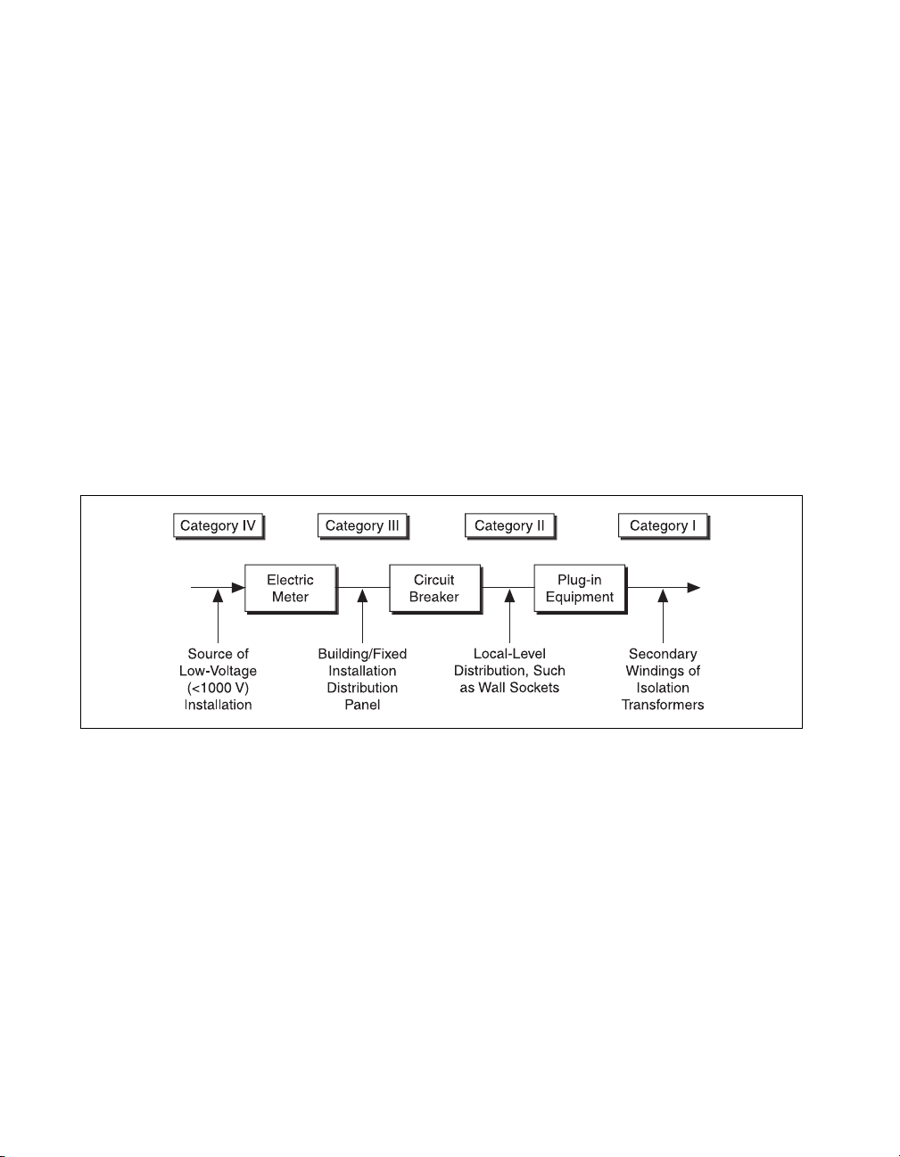
Chapter 1 Introduction
• Installation Category III is for measurements performed in the building
installation. This category is a distribution level referring to hardwired
equipment that does not rely on standard building insulation.
Examples of Installation Category III include measurements on
distribution circuits and circuit breakers. Other examples of
Installation Category III are wiring including cables, bus-bars, junction
boxes, switches, socket outlets in the building/fixed installation, and
equipment for industrial use, such as stationary motors with a
permanent connection to the building/fixed installation.
• Installation Category IV is for measurements performed at the source
of the low-voltage (<1,000 V) installation.
Examples of Installation Category IV are electric meters, and
measurements on primary overcurrent protection devices and
ripple-control units.
Below is a diagram of a sample installation.
AT E Series User Manual 1-8 ni.com
Page 21

Installing and Configuring the
Device
This chapter explains how to install and configure the AT E Series device.
Installing the Software
Complete the following steps to install the software before installing the
DAQ device.
1. Install the application development environment (ADE), such as
LabVIEW or Measurement Studio, according to the instructions on
the CD and the release notes.
2. Install NI-DAQ according to the instructions on the CD and the DAQ
Quick Start Guide included with the device.
Note
It is important to install NI-DAQ before installing the DAQ device to ensure that the
device is properly detected.
2
Installing the Hardware
You can install an AT E Series device in any available expansion slot in the
PC. However, to achieve best noise performance, you should leave as much
room as possible between the AT E Series device and other devices and
hardware. The following are general installation instructions, but consult
the PC user manual or technical reference manual for specific instructions
and warnings.
1. Write down the AT E Series device serial number. You need this serial
number when you install and configure the software.
2. Turn off and unplug the computer.
3. Remove the top cover or access port to the I/O channel.
4. Remove the expansion slot cover on the back panel of the computer.
5. Ground yourself using a grounding strap or by holding a grounded
object. Follow the ESD protection precautions described in the
Unpacking section of Chapter 1, Introduction.
© National Instruments Corporation 2-1 AT E Series User Manual
Page 22

Chapter 2 Installing and Configuring the Device
6. Insert the AT E Series device into an EISA or 16-bit ISA slot. It may
be a tight fit, but do not force the device into place.
7. Screw the mounting bracket of the AT E Series device to the back
panel rail of the computer.
8. Visually verify the installation. Make sure the device is not touching
other devices or components and is fully inserted in the slot.
9. Replace the cover.
10. Plug in and turn on the computer.
The AT E Series device is installed. You are now ready to install and
configure the software.
Configuring the Device
Due to the DAQ-PnP features, the AT E Series devices are completely
software configurable. Two types of configuration must be performed
on the AT E Series devices—bus-related configuration and data
acquisition-related configuration. Bus-related configuration includes
setting the base I/O address, DMA channels, and interrupt channels. Data
acquisition-related configuration, explained in Chapter 3, Hardware
Overview, includes such settings as AI polarity and range, AO reference
source, and other settings. For more information about data
acquisition-related configuration, refer to the NI-DAQ user manual.
Bus Interface
The AT E Series devices work in either a Plug and Play mode or a
switchless mode. These modes dictate how the base I/O address, DMA
channels, and interrupt channels are determined and assigned to the device.
Plug and Play
The AT E Series devices are fully compatible with the industry-standard
Plug and Play ISA specification. A Plug and Play system arbitrates and
assigns resources through software, freeing you from manually setting
switches and jumpers. These resources include the device base I/O address,
DMA channels, and interrupt channels. Each AT E Series device is
configured at the factory to request these resources from the Plug and Play
Configuration Manager.
The Configuration Manager receives all of the resource requests at start up,
compares the available resources to those requested, and assigns the
available resources as efficiently as possible to the Plug and Play devices.
AT E Series User Manual 2-2 ni.com
Page 23

Chapter 2 Installing and Configuring the Device
Application software can query the Configuration Manager to determine
the resources assigned to each device without your involvement. The Plug
and Play software is installed as a device driver or as an integral component
of the computer BIOS.
Switchless Data Acquisition
You can use an AT E Series device in a non-Plug and Play system as a
switchless DAQ device. A non-Plug and Play system is a system in which
the Configuration Manager has not been installed and which does not
contain any non-NI Plug and Play products. You use a configuration utility
to enter the base address, DMA, and interrupt selections, and the
application software assigns them to the device.
Note
Avoid resource conflicts with non-NI devices. For example, do not configure two
devices for the same base address.
Base I/O Address Selection
The AT E Series devices can be configured to use base addresses in the
range of 20 to FFE0 hex. Each AT E Series device occupies 32 bytes of
address space and must be located on a 32-byte boundary. Therefore, valid
addresses include 100, 120, 140, ..., 3C0, 3E0 hex. This selection is
software configured and does not require you to manually change any
settings on the device.
DMA Channel Selection
The AT E Series devices can achieve high transfer rates by using up to
three 16-bit DMA channels. You can use these DMA channels for data
transfers with the AI, AO, and general-purpose counter sections of the
device. The AT E Series devices can use only 16-bit DMA channels, which
correspond to channels 5, 6, and 7 in an ISA computer and channels 0, 1,
2, 3, 5, 6, and 7 in an EISA computer. These selections are all software
configured and do not require you to manually change any settings on the
device.
Interrupt Channel Selection
The AT E Series devices can increase bus efficiency by using an interrupt
channel. You can use an interrupt channel for event notification without the
use of polling techniques. AT E Series devices can use interrupt channels
3, 4, 5, 7, 10, 11, 12, and 15. These selections are all software configured
and do not require you to manually change any settings on the device.
© National Instruments Corporation 2-3 AT E Series User Manual
Page 24

Chapter 2 Installing and Configuring the Device
The following tables provide information concerning possible conflicts
when configuring the AT E Series device.
I/O Address Range (Hex) Device
100 to 1EF —
1F0 to 1F8 IBM PC AT Fixed Disk
200 to 20F PC and PC AT Game Controller, reserved
210 to 213 PC-DIO-24 (default)
218 to 21F —
220 to 23F Previous generation of AT-MIO devices
240 to 25F AT-DIO-32F (default)
260 to 27F Lab-PC/PC+ (default)
278 to 28F AT Parallel Printer Port 2 (LPT2)
Table 2-1. PC AT I/O Address Map
(default)
279 Reserved for Plug and Play operation
280 to 29F WD EtherCard+ (default)
2A0to2BF —
2E2to2F7 —
2F8to2FF PC,ATSerialPort2(COM2)
300 to 30F 3Com EtherLink (default)
310 to 31F —
320 to 32F ICMPC/XTFixedDiskController
330 to 35F —
360 to 363 PC Network (low address)
364 to 367 Reserved
368 to 36B PC Network (high address)
36C to 36F Reserved
370 to 366 PC, AT Parallel Printer Port 1 (LPT1)
AT E Series User Manual 2-4 ni.com
Page 25

Chapter 2 Installing and Configuring the Device
Table 2-1. PC AT I/O Address Map (Continued)
I/O Address Range (Hex) Device
380 to 38C SDLC Communications
380 to 389 Bisynchronous (BSC) Communications
(alternate)
390 to 393 Cluster Adapter 0
394 to 39F —
3A0 to 3A9 BSC Communications (primary)
3AA to 3AF —
3B0to3BF Monochrome Display/Parallel Printer
Adapter 0
3C0to3CF Enhanced Graphics Adapter, VGA
3D0to3DF Color/Graphics Monitor Adapter, VGA
3E0to3EF —
3F0 to 3F7 Diskette Controller
3F8to3FF Serial Port 1 (COM1)
A79 Reserved for Plug and Play operation
Table 2-2. PC AT Interrupt Assignment Map
IRQ Device
15 Available
14 FixedDiskController
13 Coprocessor
12 AT-DIO-32F (default)
11 AT-DIO-32F (default)
10 AT-MIO-16 (default)
9 PC Network (default)
PC Network Alternate (default)
8 Real Time Clock
© National Instruments Corporation 2-5 AT E Series User Manual
Page 26
Chapter 2 Installing and Configuring the Device
IRQ Device
Table 2-2. PC AT Interrupt Assignment Map (Continued)
7 Parallel Port 1 (LPT1)
6 Diskette Drive Controller
Fixed Disk and Diskette Drive Controller
5 Parallel Port 2 (LPT2)
PC-DIO-24 (default)
Lab-PC/PC+ (default)
4 Serial Port 1 (COM1)
BSC, BSC Alternate
3 Serial Port 2 (COM2)
BSC, BSC Alternate
Cluster (primary)
PC Network, PC Network Alternate
WD EtherCard+ (default)
3Com EtherLink (default)
2 IRQ 8–15 Chain (from interrupt controller 2)
1 Keyboard Controller Output Buffer Full
0 Timer Channel 0 Output
Table 2-3. PC AT 16-bit DMA Channel Assignment Map
Channel Device
7 AT-MIO-16 series (default)
6 AT-MIO-16 series (default)
AT-DIO-32F (default)
5 AT-DIO-32F (default)
4 Cascade for DMA Controller #1
(channels 0 through 3)
Note
EISA computers also have channels 0–3 available as 16-bit DMA channels.
AT E Series User Manual 2-6 ni.com
Page 27
Hardware Overview
This chapter presents an overview of the hardware functions on
the AT E Series device.
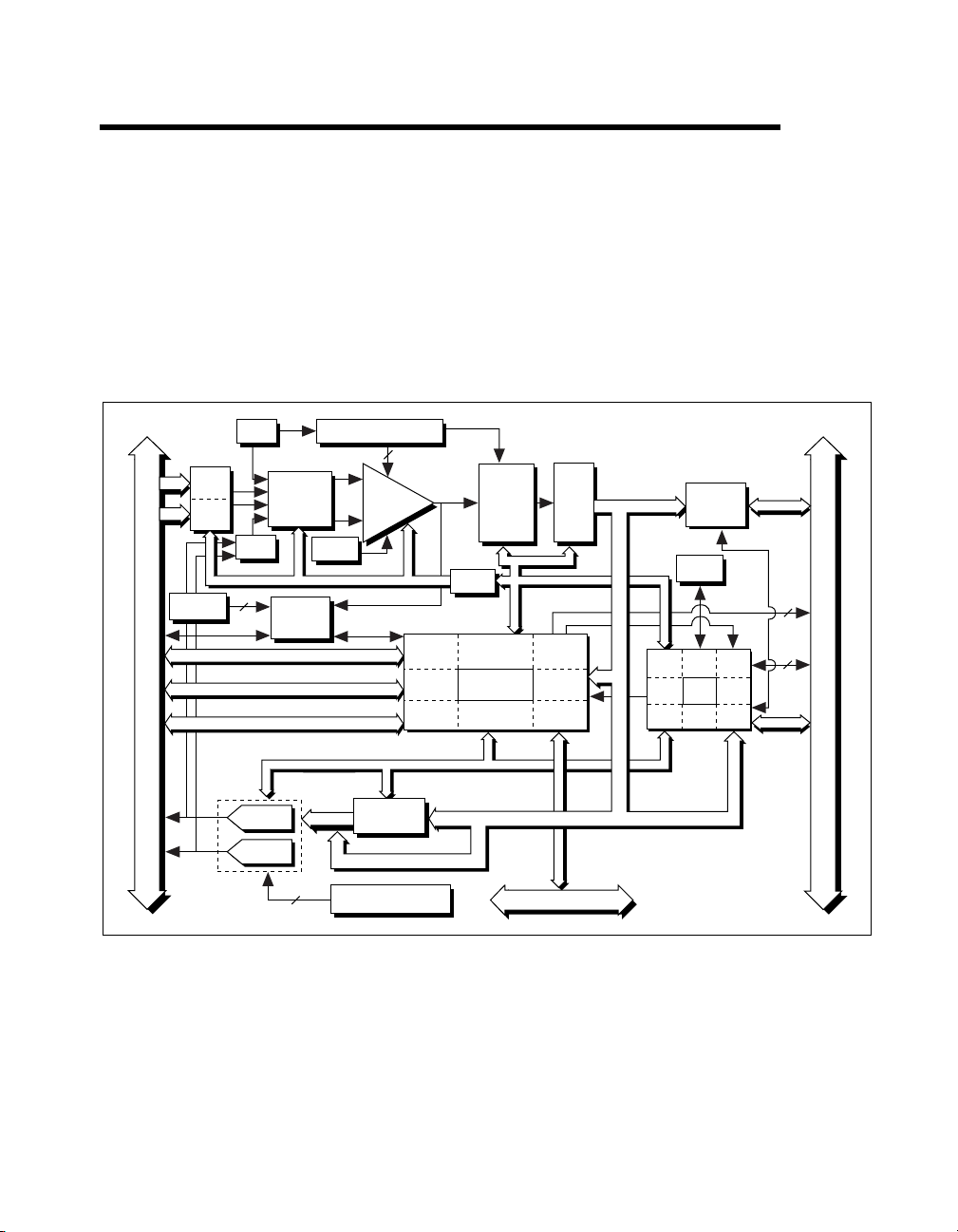
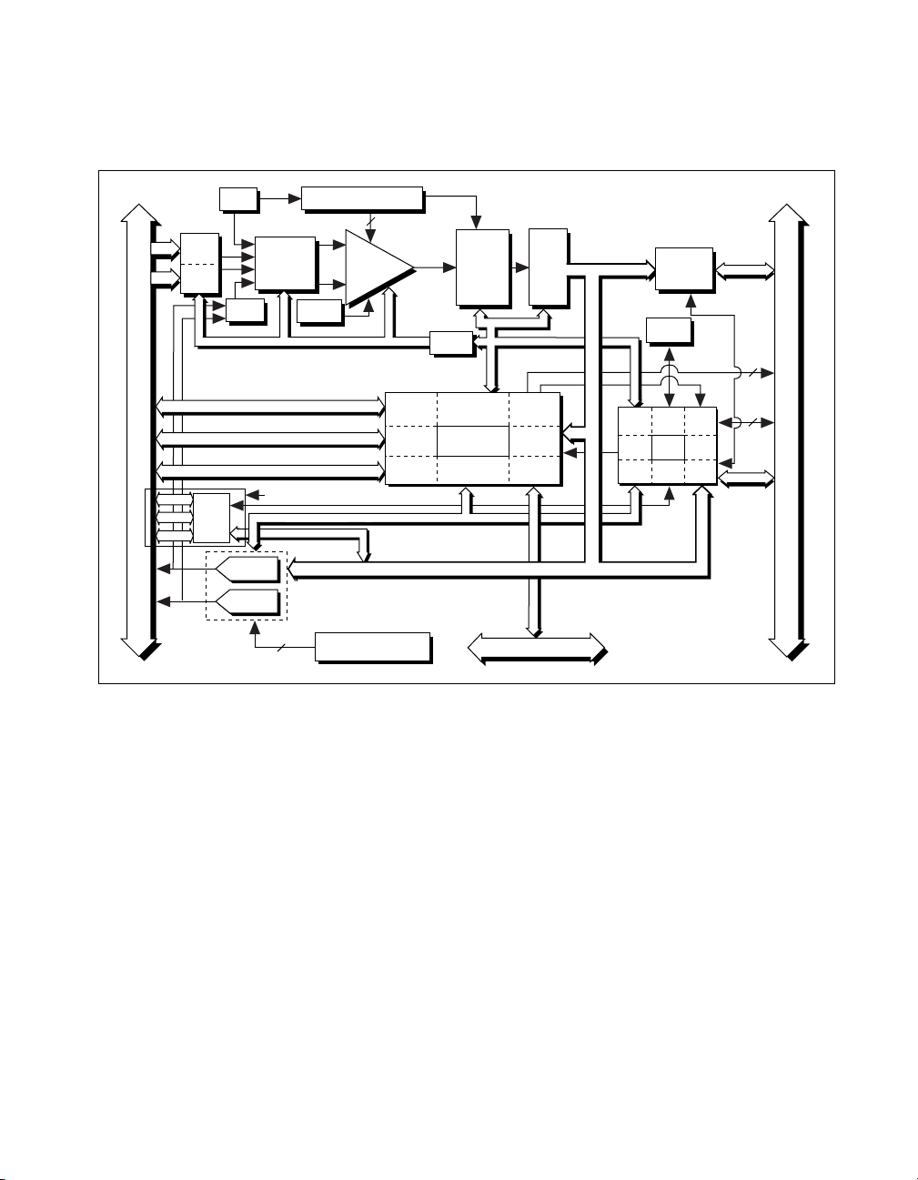
Figure 3-1 shows the block diagram for the AT-MIO-16E-1 and
AT-MIO-16E-2.
3
(8)
Analog
Muxes
(8)
Trigger Level
DACs
Trigger
PFI / Trigger
I/O Connector
Digital I/O (8)
Calibration
Timing
Voltage
REF
Mux
2
DAC0
DAC1
Mux Mode
Selection
Switches
Analog
Trigger
Circuitry
6
Dither
Circuitry
Calibration
DACs
3
+
NI-PGIA
Gain
Amplifier
–
DAC
FIFO
Calibration
DACs
Trigger
Counter/
Timing I/O
Digital I/O
Sampling
Converter
Configuration
Memory
Analog Input
Timing/Control
DAQ - STC
Analog Output
Timing/Control
AO Control
Data (16)
12-Bit
A/D
ADC
FIFO
AI Control
DMA/
Interrupt
Request
Bus
Interface
RTSI Bus
Interface
RTSI Bus
Data (16)
IRQ
DMA
Analog
Input
Control
DAQ-STC
Bus
Interface
Analog
Output
Control
Transceivers
EEPROM
EEPROM
Control
DAQ-PnP
8255
DIO
Control
Data
DMA
Interface
Plug
Play
Interface
Figure 3-1. AT-MIO-16E-1 and AT-MIO-16E-2 Block Diagram
8
3
and
Bus
AT – I/O Channel
© National Instruments Corporation 3-1 AT E Series User Manual
Page 28

Chapter 3 Hardware Overview
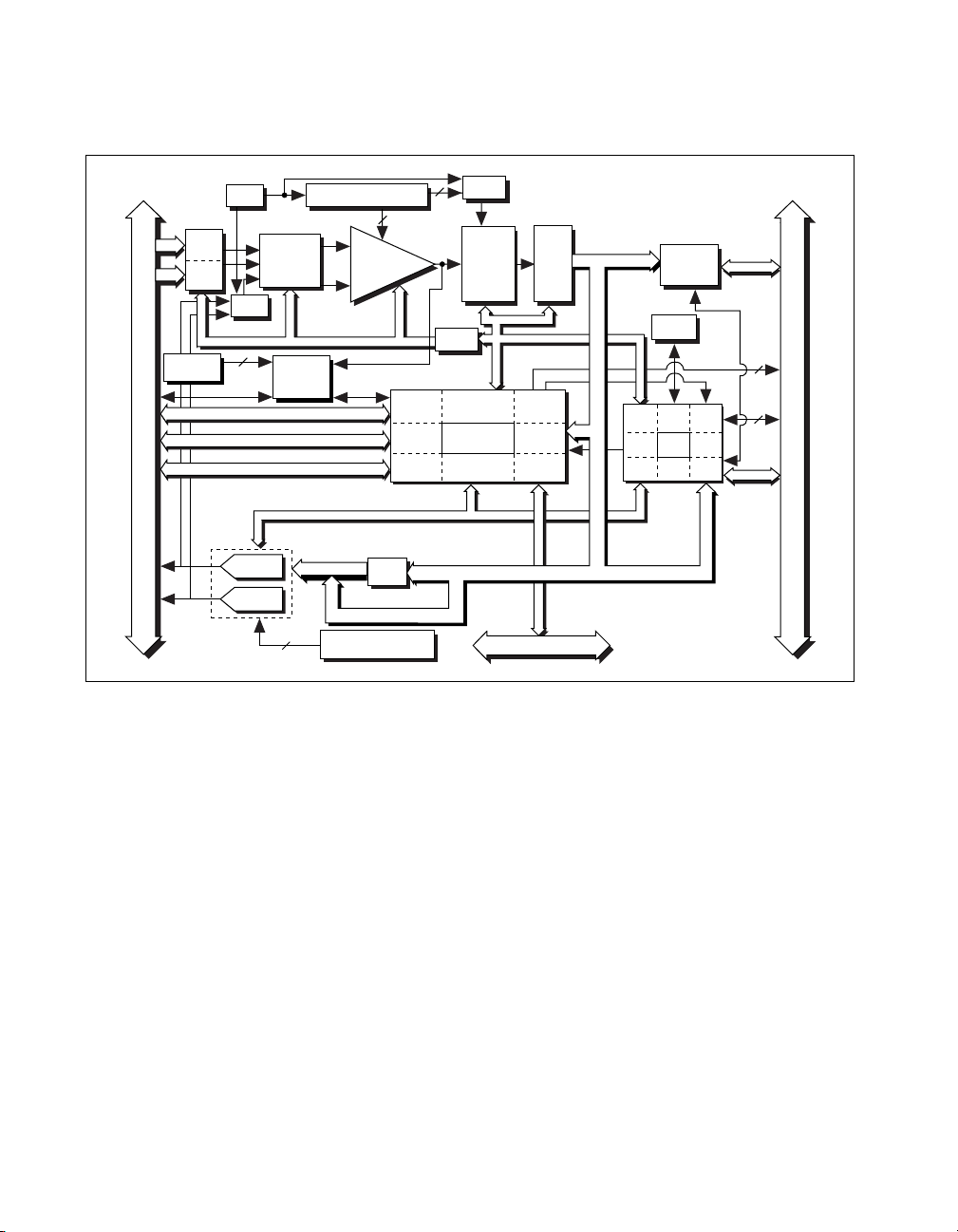
Figure 3-2 shows the block diagram for the AT-MIO-64E-3.
(32)
Analog
Muxes
(32)
Trigger Level
DACs
Trigger
PFI / Trigger
Timing
I/O Connector
Digital I/O (8)
Voltage
REF
Calibration
Mux
2
DAC0
DAC1
Mux Mode
Selection
Switches
Analog
Trigger
Circuitry
6
Dither
Circuitry
Calibration
DACs
+
NI-PGIA
Gain
Amplifier
–
DAC
FIFO
Calibration
DACs
3
12-Bit
Trigger
Counter/
Timing I/O
Digital I/O
Sampling
Converter
Configuration
Memory
Analog Input
Timing/Control
DAQ - STC
Analog Output
Timing/Control
AO Control
Data (16)
A/D
AI Control
DMA/
Interrupt
Request
Bus
Interface
RTSI Bus
Interface
ADC
FIFO
Data (16)
IRQ
DMA
RTSI Bus
Figure 3-2. AT-MIO-64E-3 Block Diagram
Analog
Input
Control
DAQ-STC
Bus
Interface
Analog
Output
Control
Transceivers
EEPROM
EEPROM
Control
DAQ-PnP
8255
DIO
Control
Data
DMA
Interface
Plug
and
Play
Bus
Interface
8
3
AT – I/O Channel
AT E Series User Manual 3-2 ni.com
Page 29
Chapter 3 Hardware Overview
Figure 3-3 shows the block diagram for the AT-MIO-16E-10 and
AT-MIO-16DE-10.
(8)
Analog
Muxes
(8)
PFI / Trigger
PA (8)
PB (8)
PC (8)
Timing
Digital I/O (8)
8255
DIO
Port
I/O Connector
Voltage
REF
Calibration
Mux
DAC0
DAC1
Calibration
Mux Mode
Selection
Switches
Dither
Circuitry
AT-MIO-16DE-10 ONLY
Data (8)
Calibration
6
DACs
4
+
NI-PGIA
Gain
Amplifier
–
DACs
Trigger
Counter/
Timing I/O
Digital I/O
Sampling
Converter
Configuration
Memory
Analog Input
Timing/Control
DAQ - STC
Analog Output
Timing/Control
AO Control
Data (16)
12-Bit
A/D
FIFO
AI Control
DMA/
Interrupt
Request
Bus
Interface
RTSI Bus
Interface
RTSI Bus
ADC
Data (16)
IRQ
DMA
Analog
Input
Control
DAQ-STC
Bus
Interface
Analog
Output
Control
Transceivers
EEPROM
EEPROM
Control
DAQ-PnP
8255
DIO
Control
Data
DMA
Interface
Plug
and
Play
Bus
Interface
Figure 3-3. AT-MIO-16E-10 and AT-MIO-16DE-10 Block Diagram
8
3
AT – I/O Channel
The primary differences between the AT-MIO-16E-10 and the
AT-MIO-16DE-10 are in the 8255 DIO port, which is not present on
the AT-MIO-16E-10, and the I/O connector.
© National Instruments Corporation 3-3 AT E Series User Manual
Page 30
Chapter 3 Hardware Overview
Voltage
REF
(8)
Analog
Muxes
(8)
Trigger Level
DACs
Trigger
PFI / Trigger
Digital I/O (8)
I/O Connector
Timing
Calibration
Mux
2
Mux Mode
Selection
Switches
Figure 3-4 shows a block diagram for the AT-MIO-16XE-10.
REF
2
Sampling
Converter
Configuration
Memory
Analog Input
Timing/Control
DAQ - STC
Analog Output
Timing/Control
AO Control
Buffer
16-Bit
AI Control
DMA/
Interrupt
Request
Bus
Interface
RTSI Bus
Interface
ADC
FIFO
Data (16)
IRQ
DMA
A/D
Analog
Input
Control
DAQ-STC
Bus
Interface
Analog
Output
Control
Transceivers
EEPROM
EEPROM
Control
DAQ-PnP
8255
DIO
Control
Data
DMA
Interface
Plug
and
Play
Bus
Interface
Analog
Trigger
Circuitry
Calibration
DACs
+
Programmable
Gain
Amplifier
–
3
Trigger
Counter/
Timing I/O
Digital I/O
8
7
AT – I/O Channel
DAC0
DAC1
DAC
FIFO
4
Calibration
DACs
Data (16)
RTSI Bus
Figure 3-4. AT-MIO-16XE-10 Block Diagram
AT E Series User Manual 3-4 ni.com
Page 31

(8)
Analog
Muxes
(8)
Trigger Level
DACs
Trigger
PFI / Trigger
I/O Connector
Digital I/O (8)
Voltage
Timing
REF
Calibration
Mux
2
Chapter 3 Hardware Overview
Figure 3-5 shows a block diagram for the AT-AI-16XE-10.
REF
2
Sampling
Converter
Configuration
Memory
Analog Input
Timing/Control
DAQ - STC
Analog Output
Timing/Control
Buffer
16-Bit
AI Control
DMA/
Interrupt
Request
Bus
Interface
RTSI Bus
Interface
ADC
FIFO
Transceivers
EEPROM
Data (16)
IRQ
DMA
Analog
EEPROM
Input
Control
Control
DAQ-STC
Bus
DAQ-PnP
Interface
Analog
8255
Output
DIO
Control
Control
Data (16)
A/D
RTSI Bus
Mux Mode
Selection
Switches
Analog
Trigger
Circuitry
Calibration
DACs
+
Programmable
Gain
Amplifier
–
3
Timing I/O
Digital I/O
Trigger
Counter/
Data
DMA
Interface
Plug
and
Play
Bus
Interface
8
7
AT – I/O Channel
Figure 3-5.
AT-AI-16XE-10 Block Diagram
© National Instruments Corporation 3-5 AT E Series User Manual
Page 32

Chapter 3 Hardware Overview
Figure 3-6 shows a block diagram for the AT-MIO-16XE-50.
(8)
Analog
Muxes
(8)
PFI / Trigger
Timing
Digital I/O (8)
I/O Connector
Voltage
REF
Calibration
Mux
DAC0
DAC1
Mux Mode
Selection
Switches
4
Calibration
DACs
+
Programmable
Gain
Amplifier
–
Calibration
DACs
Sampling
Converter
Configuration
Memory
Analog Input
Timing/Control
DAQ - STC
Analog Output
Timing/Control
AO Control
Data (16)
2
16-Bit
A/D
FIFO
AI Control
DMA/
Interrupt
Request
Bus
Interface
RTSI Bus
Interface
RTSI Bus
ADC
Data (16)
IRQ
DMA
Analog
Control
DAQ-STC
Interface
Analog
Output
Control
3
Trigger
Counter/
Timing I/O
Digital I/O
Figure 3-6. AT-MIO-16XE-50 Block Diagram
Input
Bus
Transceivers
EEPROM
EEPROM
Control
DAQ-PnP
8255
DIO
Control
Data
DMA
Interface
Plug
and
Play
Bus
Interface
8
3
I/O Channel
AT –
Analog Input
The AI section of each AT E Series device is software configurable.
You can select different AI configurations through application software
designed to control the AT E Series devices. The following sections
describe in detail each of the AI categories.
Input Mode
The AT E Series devices have three different input modes—nonreferenced
single-ended (NRSE) input, referenced single-ended (RSE) input, and
differential (DIFF) input. The single-ended input configurations use up
to 16 channels (64 channels on the AT-MIO-64E-3). The DIFF input
configurationusesuptoeightchannels(32channelsonthe
AT-MIO-64E-3). Input modes are programmed on a per channel basis for
multimode scanning. For example, you can configure the circuitry to scan
AT E Series User Manual 3-6 ni.com
Page 33

Chapter 3 Hardware Overview
12 channels—four differentially configured channels and eight
single-ended channels. Table 3-1 describes the three input configurations.
Table 3-1.
Available Input Configurations for the AT E Series
Configuration Description
DIFF A channel configured in DIFF mode uses two analog
channel input lines. One line connects to the positive
input of the device programmable gain
instrumentation amplifier (PGIA), and the other
connects to the negative input of the PGIA.
RSE A channel configured in RSE mode uses one analog
channel input line, which connects to the positive
input of the PGIA. The negative input of the PGIA
is internally tied to AI ground (AIGND).
NRSE A channel configured in NRSE mode uses one analog
channel input line, which connects to the positive
input of the PGIA. The negative input of the PGIA
connects to the AI sense (AISENSE) input.
For more information about the three types of input configuration, refer to
the Analog Input Signal Connections section of Chapter 4, Connecting
Signals, which contains diagrams showing the signal paths for the three
configurations.
Input Polarity and Input Range
♦ AT-MIO-16E-1, AT-MIO-16E-2, AT-MIO-64E-3, AT-MIO-16E-10, and
AT-MIO-16DE-10
These devices have two input polarities—unipolar and bipolar. Unipolar
input means that the input voltage range is between 0 and V
is a positive reference voltage. Bipolar input means that the input voltage
range is between –V
/2 and +V
ref
/2. The AT-MIO-16E-1,
ref
AT-MIO-16E-2, AT-MIO-64E-3, AT-MIO-16E-10, and
AT-MIO-16DE-10 have a unipolar input range of 10 V (0 to 10 V) and a
bipolar input range of 10 V (±5 V). You can program polarity and range
settings on a per channel basis so that you can configure each input channel
uniquely.
The software-programmable gain on these devices increases their overall
flexibility by matching the input signal ranges to those that the ADC can
accommodate. The AT-MIO-16E-1, AT-MIO-16E-2, AT-MIO-64E-3,
© National Instruments Corporation 3-7 AT E Series User Manual
, where V
ref
ref
Page 34

Chapter 3 Hardware Overview
AT-MIO-16E-10, and AT-MIO-16DE-10 have gains of 0.5, 1, 2, 5, 10, 20,
50, and 100 and are suited for a wide variety of signal levels. With the
proper gain setting, you can use the full resolution of the ADC to measure
the input signal. Table 3-2 shows the overall input range and precision
according to the input range configuration and gain used.
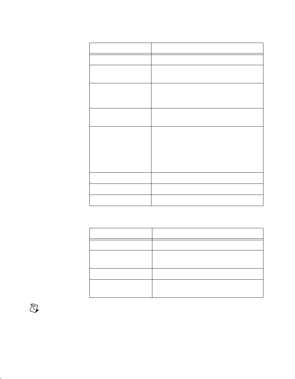
Table 3-2. Actual Range and Measurement Precision
Range
Configuration
0to+10V 1.0
–5 to +5 V 0.5
1
The value of 1 LSB of the 12-bit ADC; that is, the voltage increment corresponding to a
change of one count in the ADC 12-bit count.
Note: Refer to Appendix A, Specifications, for absolute maximum ratings.
Gain Actual Input Range Precision
0to+10V
2.0
5.0
10.0
20.0
50.0
100.0
0to+5V
0to+2V
0to+1V
0to+500mV
0to+200mV
0to+100mV
–10to+10V
1.0
2.0
5.0
10.0
20.0
50.0
100.0
–5 to +5 V
–2.5to+2.5V
–1 to +1 V
–500 to +500 mV
–250 to +250 mV
–100 to +100 mV
–50 to +50 mV
♦ AT-MIO-16XE-10, AT-AI-16XE-10, AT-MIO-16XE-50
1
2.44 mV
1.22 mV
488.28 µV
244.14 µV
122.07 µV
48.83 µV
24.41 µV
4.88 mV
2.44 mV
1.22 mV
488.28 µV
244.14 µV
122.07 µV
48.83 µV
24.41 µV
These devices have two input polarities—unipolar and bipolar. Unipolar
input means that the input voltage range is between 0 and V
, where V
ref
ref
is a positive reference voltage. Bipolar input means that the input voltage
range is between –V
and +V
ref
. The AT-MIO-16XE-10, AT-AI-16XE-10,
ref
and AT-MIO-16XE-50 have a unipolar input range of 10 V (0 to 10 V) and
a bipolar input range of 20 V (±10 V). You can program polarity and range
settings on a per channel basis so that you can configure each input channel
uniquely.
AT E Series User Manual 3-8 ni.com
Page 35

Chapter 3 Hardware Overview
Note
You can calibrate the AT-MIO-16XE-10, AT-AI-16XE-10, and AT-MIO-16XE-50
AI circuitry for either a unipolar or bipolar polarity. If you mix unipolar and bipolar
channels in the scan list and you are using NI-DAQ, then NI-DAQ loads the calibration
constants appropriate to the polarity for which AI channel 0 is configured.
The software-programmable gain on these devices increases their overall
flexibility by matching the input signal ranges to those that the ADC can
accommodate. The AT-MIO-16XE-10 and AT-AI-16XE-10 have gains of
1, 2, 5, 10, 20, 50, and 100 and the AT-MIO-16XE-50 has gains of 1, 2, 10,
and 100. These gains are suited for a wide variety of signal levels. With the
proper gain setting, you can use the full resolution of the ADC to measure
the input signal. Table 3-3 shows the overall input range and precision
according to the input range configuration and gain used.
Table 3-3. Actual Range and Measurement Precision for the AT-MIO-16XE-10,
AT-AI-16XE-10, and AT-MIO-16XE-50
Range
Configuration
0to+10V 1.0
–10 to +10 V 1.0
1
The value of 1 LSB of the 16-bit ADC; that is, the voltage increment corresponding to a
change of one count in the ADC 16-bit count.
2
AT-MIO-16XE-10 and AT-AI-16XE-10 only
Note: Refer to Appendix A, Specifications, for absolute maximum ratings.
Gain Actual Input Range Precision
2.0
5.0
10.0
20.0
50.0
100.0
2.0
5.0
10.0
20.0
50.0
100.0
2
2
2
2
2
2
2
2
2
2
2
2
2
2
0to+10V
0to+5V
0to+2V
0to+1V
0 to +500 mV
0 to +200 mV
0 to 100 mV
–10 to +10 V
–5to+5V
–2to+2V
–1to+1V
–500 to +500 mV
–200 to +200 mV
–100 to +100 mV
152.59 µV
76.29 µV
30.52 µV
15.26 µV
.63 µV
3.05 µV
1.53 µV
305.18 µV
152.59 µV
61.04 µV
30.52 µV
15.26 µV
6.10 µV
3.05 µV
1
© National Instruments Corporation 3-9 AT E Series User Manual
Page 36

Chapter 3 Hardware Overview
Dither
Considerations for Selecting Input Ranges
Which input polarity and range you select depends on the expected range
of the incoming signal. A large input range can accommodate a large signal
variation but reduces the voltage resolution. Choosing a smaller input range
improves the voltage resolution but may result in the input signal going out
of range. For best results, you should match the input range as closely as
possible to the expected range of the input signal. For example, if you are
certain the input signal is not negative (below 0 V), unipolar input polarity
is best. However, if the signal is negative or equal to zero, inaccurate
readings occur if you use unipolar input polarity.
When you enable dither, you add approximately 0.5 LSB
Gaussian noise to the signal to be converted by the ADC. This addition
is useful for applications involving averaging to increase the resolution
of the AT E Series device, as in calibration or spectral analysis. In such
applications, noise modulation is decreased and differential linearity is
improved by the addition of the dither. When taking DC measurements,
such as when checking the device calibration, you should enable dither and
average about 1,000 points to take a single reading. This process removes
the effects of quantization and reduces measurement noise, resulting in
improved resolution. For high-speed applications not involving averaging
or spectral analysis, you may want to disable the dither to reduce noise. You
enable and disable the dither circuitry through software.
rms
of white
Figure 3-7 illustrates the effect of dither on signal acquisition. Figure 3-7a
shows a small (±4 LSB) sine wave acquired with dither off. The
quantization of the ADC is clearly visible. Figure 3-7b shows what happens
when 50 such acquisitions are averaged together; quantization is still
plainly visible. In Figure 3-7c, the sine wave is acquired with dither on.
There is a considerable amount of noise visible. But averaging about 50
such acquisitions, as shown in Figure 3-7d, eliminates both the added noise
and the effects of quantization. Dither has the effect of forcing quantization
noise to become a zero-mean random variable rather than a deterministic
function of the input signal.
AT E Series User Manual 3-10 ni.com
Page 37

Chapter 3 Hardware Overview
LSBs
6.0
4.0
2.0
0.0
–2.0
–4.0
–6.0
100 200 300 4000 500
LSBs
6.0
4.0
2.0
0.0
–2.0
–4.0
–6.0
100 200 400
100 200 300 4000 500
a. Dither disabled; no averaging b. Dither disabled; average of 50 acquisitions
LSBs
6.0
4.0
2.0
0.0
–2.0
–4.0
–6.0
100 200 300 4000 500
c. Dither enabled; no averaging
LSBs
6.0
4.0
2.0
0.0
–2.0
–4.0
–6.0
100 200 300 4000 500
d. Dither enabled; average of 50 acquisitions
Figure 3-7. Dither
You cannot disable dither on the AT-MIO-16XE-10, AT-AI-16XE-10, or
AT-MIO-16XE-50. This is because the resolution of the ADC is so fine that
the ADC and the PGIA inherently produce almost 0.5 LSB
of noise. This
rms
is equivalent to having a dither circuit that is always enabled.
Multiple-Channel Scanning Considerations
All of the AT E Series devices can scan multiple channels at the same
maximum rate as their single-channel rate; however, you should pay
careful attention to the settling times for each of the devices. The settling
time for most of the AT E Series devices is independent of the selected
gain, even at the maximum sampling rate. The settling time for the high
channel count and very high-speed devices is gain dependent, which can
affect the useful sampling rate for a given gain. No extra settling time is
necessary between channels as long as the gain is constant and source
impedances are low. Refer to Appendix A, Specifications, for a complete
listing of settling times for each of the AT E Series devices.
© National Instruments Corporation 3-11 AT E Series User Manual
Page 38

Chapter 3 Hardware Overview
When scanning among channels at various gains, the settling times may
increase. When the PGIA switches to a higher gain, the signal on the
previous channel may be well outside the new, smaller range. For instance,
suppose a 4 V signal is connected to channel 0 and a 1 mV signal is
connected to channel 1, and suppose the PGIA is programmed to apply
a gain of one to channel 0 and a gain of 100 to channel 1. When the
multiplexer switches to channel 1 and the PGIA switches to a gain of 100,
the new full-scale range is 100 mV (if the ADC is in unipolar mode).
The approximately 4 V step from 4 V to 1 mV is 4,000% of the new
full-scale range. For a 12-bit device to settle within 0.012% (120 ppm or
1/2 LSB) of the 100 mV full-scale range on channel 1, the input circuitry
has to settle to within 0.0003% (3 ppm or 1/80 LSB) of the 4 V step. It may
take as long as 100 µs for the circuitry to settle this much. For a 16-bit
device to settle within 0.0015% (15 ppm or 1 LSB) of the 100 mV full-scale
range on channel 1, the input circuitry has to settle within 0.00004%
(0.4 ppm or 1/400 LSB) of the 4 V step. It may take as long as 200 µs for
the circuitry to settle this much. In general, this extra settling time is not
needed when the PGIA is switching to a lower gain.
Settling times can also increase when scanning high-impedance signals due
to a phenomenon called charge injection, where the AI multiplexer injects
a small amount of charge into each signal source when that source is
selected. If the impedance of the source is not low enough, the effect of the
charge—a voltage error—does not have decayed by the time the ADC
samples the signal. For this reason, you should keep source impedances
under 1 kΩ to perform high-speed scanning.
Due to the previously described limitations of settling times resulting from
these conditions, multiple-channel scanning is not recommended unless
sampling rates are low enough or it is necessary to sample several signals
as nearly simultaneously as possible. The data is much more accurate and
channel-to-channel independent if you acquire data from each channel
independently (for example, 100 points from channel 0, then 100 points
from channel 1, then 100 points from channel 2, and so on).
AT E Series User Manual 3-12 ni.com
Page 39

Analog Output
♦ AT-MIO-16E-1, AT-MIO-16E-2, AT-MIO-64E-3, AT-MIO-16E-10, and
AT-MIO-16DE-10
The AT E Series devices supply two channels of AO voltage at the I/O
connector. You can select the reference and range for the AO circuitry
through software. The reference can be either internal or external, whereas
the range can be either bipolar or unipolar.
♦ AT-MIO-16XE-50
The AT-MIO-16XE-50 supplies two channels of AO voltage at the I/O
connector. The range is fixed at bipolar ±10 V.
♦ AT-MIO-16XE-10
The AT-MIO-16XE-10 supplies two channels of AO voltage at the I/O
connector. The range is software selectable between unipolar (0 to 10 V)
and bipolar (+
Analog Output Reference Selection
♦ AT-MIO-16E-1, AT-MIO-16E-2, AT-MIO-64E-3, AT-MIO-16E-10, and
AT-MIO-16DE-10 only
10 V).
Chapter 3 Hardware Overview
You can connect each D/A converter (DAC) to the AT E Series device
internal reference of 10 V or to the external reference signal connected
to the external reference (EXTREF) pin on the I/O connector. This signal
applied to EXTREF should be between –10 and +10 V. You do not need to
configure both channels for the same mode.
Analog Output Polarity Selection
♦ AT-MIO-16E-1, AT-MIO-16E-2, AT-MIO-64E-3, AT-MIO-16E-10, and
AT-MIO-16DE-10 only
You can configure each AO channel for either unipolar or bipolar output.
A unipolar configuration has a range of 0 to V
configuration has a range of –V
reference used by the DACs in the AO circuitry and can be either the
+10 Vonboard reference or an externally supplied reference between
–10 and +10 V. You do not need to configure both channels for the same
range.
© National Instruments Corporation 3-13 AT E Series User Manual
ref
to +V
ref
at the AO. A bipolar
ref
at the AO. V
is the voltage
ref
Page 40

Chapter 3 Hardware Overview
Selecting a bipolar range for a particular DAC means that any data written
to that DAC is interpreted as two’s complement format. In two’s
complement mode, data values written to the AO channel can be either
positive or negative. If you select unipolar range, data is interpreted in
straight binary format. In straight binary mode, data values written to the
AO channel range must be positive.
♦ AT-MIO-16XE-10
You can configure each AO channel for either unipolar or bipolar output.
A unipolar configuration has a range of 0 to 10 V at the analog output.
A bipolar configuration has a range of –10 to +10 V at the analog output.
You do not need to configure both channels for the same range.
Analog Output Reglitch Selection
♦ AT-MIO-16E-1, AT-MIO-16E-2, and AT-MIO-64E-3 only
In normal operation, a DAC output glitches whenever it is updated with
a new value. The glitch energy differs from code to code and appears
as distortion in the frequency spectrum. Each analog output of the
AT-MIO-16E-1, AT-MIO-16E-2, and AT-MIO-64E-3 contains a reglitch
circuit that generates uniform glitch energy at every code rather than large
glitches at the major code transitions. This uniform glitch energy appears
as a multiple of the update rate in the frequency spectrum. Notice that this
reglitch circuit does not eliminate the glitches; it only makes them more
uniform in size. Reglitching is normally disabled at startup and can be
independently enabled for each channel through software.
Analog Trigger
♦ AT-MIO-16E-1, AT-MIO-16E-2, AT-MIO-64E-3, AT-MIO-16XE-10, and
AT-AI-16XE-10 only
In addition to supporting internal software triggering and external digital
triggering to initiate a data acquisition sequence, the AT-MIO-16E-1,
AT-MIO-16E-2, AT-MIO-64E-3, AT-MIO-16XE-10, and AT-AI-16XE-10
also support analog triggering. You can configure the analog trigger
circuitry to accept either a direct analog input from the PFI0/TRIG1 pin
on the I/O connector or a postgain signal from the output of the PGIA, as
shown in Figure 3-8. The trigger-level range for the direct analog channel
is ±10 V in 78 mV steps for the AT-MIO-16E-1, AT-MIO-16E-2, and
AT-MIO-64E-3, and ±10 V in 4.9 mV steps for the AT-MIO-16XE-10 and
AT-AI-16XE-10. The range for the post-PGIA trigger selection is simply
AT E Series User Manual 3-14 ni.com
Page 41

Chapter 3 Hardware Overview
the full-scale range of the selected channel, and the resolution is that
range divided by 256 for the AT-MIO-16E-1, AT-MIO-16E-2, and
AT-MIO-64E-3, and divided by 4,096 for the AT-MIO-16XE-10 and
AT-AI-16XE-10.
Note
The PFI0/TRIG1 pin is a high-impedance input. Therefore, it is susceptible to
crosstalk from adjacent pins, which can result in false triggering when the pin is left
unconnected. To avoid false triggering, make sure this pin is connected to a low-impedance
signal source (less than 10 kΩ source impedance) if you plan to enable this input using
software.
Analog
Input
Channels
PFI0/TRIG1
+
–
PGIA
Figure 3-8.
Mux
Analog Trigger Block Diagram
ADC
Analog
Trigger
Circuit
DAQ-STC
There are five analog triggering modes available, as shown in Figures 3-9
through 3-13. You can set lowValue and highValue independently in
software.
In below-low-level analog triggering mode, the trigger is generated when
the signal value is less than lowValue. HighValue is unused.
© National Instruments Corporation 3-15 AT E Series User Manual
Page 42

Chapter 3 Hardware Overview
lowValue
Trigger
Figure 3-9. Below-Low-Level Analog Triggering Mode
In above-high-level analog triggering mode, the trigger is generated when
the signal value is greater than highValue. LowValue is unused.
highValue
Trigger
Figure 3-10. Above-High-Level Analog Triggering Mode
In inside-region analog triggering mode, the trigger is generated when the
signal value is between the lowValue and the highValue.
highValue
lowValue
Trigger
Figure 3-11. Inside-Region Analog Triggering Mode
AT E Series User Manual 3-16 ni.com
Page 43

Chapter 3 Hardware Overview
In high-hysteresis analog triggering mode, the trigger is generated when the
signal value is greater than highValue, with the hysteresis specified by
lowValue.
highValue
lowValue
Trigger
Figure 3-12. High-Hysteresis Analog Triggering Mode
In low-hysteresis analog triggering mode, the trigger is generated when the
signal value is less than lowValue, with the hysteresis specified by
highValue.
highValue
lowValue
Trigger
Figure 3-13.
Low-Hysteresis Analog Triggering Mode
The analog trigger circuit generates an internal digital trigger based on the
AI signal and the user-defined trigger levels. This digital trigger can be used
by any of the timing sections of the DAQ-STC, including the AI, AO, and
general-purpose counter/timer sections. For example, the AI section can be
configured to acquire n scans after the AI signal crosses a specific
threshold. As another example, the AO section can be configured to update
its outputs whenever the AI signal crosses a specific threshold.
© National Instruments Corporation 3-17 AT E Series User Manual
Page 44

Chapter 3 Hardware Overview
Digital I/O
The AT E Series devices contain eight lines of DIO for general-purpose
use. You can individually configure each line through software for either
input or output. The AT-MIO-16DE-10 has 24 additional DIO lines,
configured as three 8-bit ports: PA<0..7>, PB<0..7>, and PC<0..7>. You
can configure each port for both input and output in various combinations,
with some handshaking capabilities. At system startup and reset, the digital
I/O ports are all high impedance.
The hardware up/down control for general-purpose counters 0 and 1 are
connected onboard to DIO6 and DIO7, respectively. Thus, you can use
DIO6 and DIO7 to control the general-purpose counters. The up/down
control signals are input only and do not affect the operation of the
DIO lines.
Timing Signal Routing
The DAQ-STC provides a very flexible interface for connecting timing
signals to other devices or external circuitry. The AT E Series device uses
the RTSI bus for interconnecting timing signals between devices and
the Programmable Function Input (PFI) pins on the I/O connector for
connecting to external circuitry. These connections are designed to enable
the AT E Series device to both control and be controlled by other devices
and circuits.
There are a total of 13 timing signals internal to the DAQ-STC that can
be controlled by an external source. These timing signals can also be
controlled by signals generated internally to the DAQ-STC, and these
selections are fully software configurable. For example, the signal routing
multiplexer for controlling the CONVERT* signal is shown in Figure 3-14.
AT E Series User Manual 3-18 ni.com
Page 45

RTSI Trigger<0..6>
PFI<0..9>
Sample Interval Counter TC
GPCTR0_OUT
Chapter 3 Hardware Overview
CONVERT*
Figure 3-14.
CONVERT* Signal Routing
This figure shows that CONVERT* can be generated from a number of
sources, including the external signals RTSI<0..6> and PFI<0..9> and the
internal signals Sample Interval Counter TC and GPCTR0_OUT.
Many of these timing signals are also available as outputs on the RTSI pins,
as indicated in the RTSI Triggers section later in this chapter, and on the PFI
pins, as indicated in Chapter 4, Connecting Signals.
© National Instruments Corporation 3-19 AT E Series User Manual
Page 46

Chapter 3 Hardware Overview
Programmable Function Inputs
The 10 PFIs are connected to the signal routing multiplexer for each timing
signal, and software can select one of the PFIs as the external source for a
given timing signal. It is important to note that any of the PFIs can be used
as an input by any of the timing signals and that multiple timing signals can
use the same PFI simultaneously. This flexible routing scheme reduces the
need to change physical connections to the I/O connector for different
applications.
You can also individually enable each of the PFI pins to output a specific
internal timing signal. For example, if you need the UPDATE* signal as an
output on the I/O connector, software can turn on the output driver for the
PFI5/UPDATE* pin. To use the PFI pins as outputs, you must use the Route
Signal VI to individually enable each of the PFI pins to output a specific
timing signal.
Device and RTSI Clocks
Many functions performed by the AT E Series devices require a frequency
timebase to generate the necessary timing signals for controlling A/D
conversions, DAC updates, or general-purpose signals at the I/O connector.
An AT E Series device can use either its internal 20 MHz timebase or a
timebase received over the RTSI bus. In addition, if you configure the
device to use the internal timebase, you can also program the device to
drive its internal timebase over the RTSI bus to another device that is
programmed to receive this timebase signal. This clock source, whether
local or from the RTSI bus, is used directly by the device as the primary
frequency source. The default configuration at startup is to use the internal
timebase without driving the RTSI bus timebase signal. You select this
timebase through software.
RTSI Triggers
The seven RTSI trigger lines on the RTSI bus provide a very flexible
interconnection scheme for any AT E Series device sharing the RTSI bus.
These bidirectional lines can drive any of eight timing signals onto the
RTSI bus and can receive any of these timing signals. This signal
connection scheme is shown in Figure 3-15.
AT E Series User Manual 3-20 ni.com
Page 47

Trigger
RTSI Bus Connector
Clock
Chapter 3 Hardware Overview
DAQ-STC
TRIG1
TRIG2
CONVERT*
UPDATE*
WFTRIG
GPCTR0_SOURCE
GPCTR0_GATE
GPCTR0_OUT
7
RTSI Switch
Switch
STARTSCAN
AIGATE
SISOURCE
UISOURCE
GPCTR1_SOURCE
GPCTR1_GATE
RTSI_OSC (20 MHz)
Figure 3-15.
RTSI Bus Signal Connection
Refer to the Timing Connections section of Chapter 4, Connecting Signals,
for a description of the signals shown in Figure 3-15.
© National Instruments Corporation 3-21 AT E Series User Manual
Page 48

Connecting Signals
This chapter describes how to make input and output signal connections to
the AT E Series device using the device I/O connector.
Table 4-1. I/O Connector Details
4
Device with
I/O Connector
68-Pin AT E
Series Device
100-Pin AT E
Series Device
Numberof
Pins
68 N/A SH6868-EP Shielded Cable,
100 SH100100 Shielded
Caution
on the devices can damage the device and the computer. Maximum input ratings for each
signal are given in Tables 4-3 through 4-6 in the Protection column. National Instruments
is not liable for any damage resulting from such signal connections.
Connections that exceed any of the maximum ratings of input or output signals
I/O Connector
Cable for Connecting
to 100-pin Accessories
Cable
Figure 4-1 shows the pin assignments for the 68-pin I/O connector on the
AT-MIO-16E-1, AT-MIO-16E-2, AT-MIO-16E-10, AT-MIO-16XE-10,
AT-AI-16XE-10, and AT-MIO-16XE-50. Figure 4-2 shows the pin
assignments for the 100-pin I/O connector on the AT-MIO-64E-3.
Figure 4-3 shows the pin assignments for the 100-pin I/O connector on
the AT-MIO-16DE-10. Refer to Appendix B, Optional Cable Connector
Descriptions, for the pin assignments for the 50-pin connectors. A signal
description follows the connector pinouts.
Cable for Connecting
to 68-pin Accessories
R6868 Ribbon Cable
SH6868R1-EP
SH1006868 Shielded Cable R1005050 Ribbon Cable
Cable for Connecting to
50-pin Signal Accessories
SH6850 Shielded Cable,
R6850 Ribbon Cable
Caution
on the AT E Series devices can damage the AT E Series device and the PC. Maximum
input ratings for each signal are given in Tables 4-3 through 4-6 in the Protection column.
NI is not liable for any damage resulting from such signal connections.
© National Instruments Corporation 4-1 AT E Series User Manual
Connections that exceed any of the maximum ratings of input or output signals
Page 49

Chapter 4 Connecting Signals
ACH8
ACH1
AIGND
ACH10
ACH3
AIGND
ACH4
AIGND
ACH13
ACH6
AIGND
ACH15
DAC0OUT
DAC1OUT
EXTREF
DIO4
DGND
DIO1
DIO6
DGND
+5V
DGND
DGND
PFI0/TRIG1
PFI1/TRIG2
DGND
+5V
DGND
PFI5/UPDATE*
PFI6/WFTRIG
DGND
PFI9/GPCTR0_GATE
GPCTR0_OUT
FREQ_OUT
1
1
2
34 68
33 67
32 66
31 65
30 64
29 63
28 62
27 61
26 60
25 59
24 58
23 57
22 56
21 55
20 54
19 53
18 52
17 51
16 50
15 49
14 48
13 47
12 46
11 45
10 44
943
842
741
640
539
438
337
236
135
ACH0
AIGND
ACH9
ACH2
AIGND
ACH11
AISENSE
ACH12
ACH5
AIGND
ACH14
ACH7
AIGND
AOGND
AOGND
DGND
DIO0
DIO5
DGND
DIO2
DIO7
DIO3
SCANCLK
EXTSTROBE*
DGND
PFI2/CONVERT*
PFI3/GPCTR1_SOURCE
PFI4/GPCTR1_GATE
GPCTR1_OUT
DGND
PFI7/STARTSCAN
PFI8/GPCTR0_SOURCE
DGND
DGND
1
Not available on AT-AI-16XE-10
2
Not available on AT-MIO-16XE-10,
AT-AI-16XE-10, or AT-MIO-16XE-50
Figure 4-1. I/O Connector Pin Assignment for the AT-MIO-16E-1, AT-MIO-16E-2,
AT-MIO-16E-10, AT-MIO-16XE-10, AT-AI-16XE-10, and AT-MIO-16XE-50
AT E Series User Manual 4-2 ni.com
Page 50

Chapter 4 Connecting Signals
AIGND ACH16
AIGND ACH24
ACH10 ACH27
ACH11 ACH28
ACH12 ACH29
ACH13 ACH30
ACH14 ACH31
ACH15 ACH40
AISENSE ACH33
DAC0OUT ACH41
DAC1OUT ACH34
EXTREF ACH42
AOGND ACH35
DGND ACH43
DGND ACH39
SCANCLK ACH56
EXTSTROBE* ACH49
FI0/TRIG1 ACH57
PFI1/TRIG2 ACH50
PFI2/CONVERT* ACH58
PFI3/GPCTR1_SOURCE ACH51
PFI4/GPCTR1_GATE ACH59
GPCTR1_OUT ACH52
PFI5/UPDATE* ACH60
PFI6/WFTRIG ACH53
PFI7/STARTSCAN ACH61
PFI8/GPCTR0_SOURCE ACH54
PFI9/GPCTR0_GATE ACH62
GPCTR0_OUT ACH55
FREQ_OUT ACH63
151
252
ACH0 ACH17
353
ACH8 ACH25
454
ACH1 ACH18
555
ACH9 ACH26
656
ACH2 ACH19
757
858
ACH3 ACH20
959
10 60
ACH4 ACH21
11 61
12 62
ACH5 ACH22
13 63
14 64
ACH6 ACH23
15 65
16 66
ACH7 ACH32
17 67
18 68
19 69
20 70
21 71
22 72
23 73
24 74
DIO0 AISENSE2
25 75
DIO4 AIGND
26 76
DIO1 ACH36
27 77
DIO5 ACH44
28 78
DIO2 ACH37
29 79
DIO6 ACH45
30 80
DIO3 ACH38
31 81
DIO7 ACH46
32 82
33 83
+5V ACH47
34 84
+5V ACH48
35 85
36 86
37 87
38 88
39 89
40 90
41 91
42 92
43 93
44 94
45 95
46 96
47 97
48 98
49 99
50 100
Figure 4-2. I/O Connector Pin Assignment for the AT-MIO-64E-3
© National Instruments Corporation 4-3 AT E Series User Manual
Page 51

Chapter 4 Connecting Signals
AIGND PC7
AIGND GND
ACH10 GND
ACH11 GND
ACH12 GND
ACH13 GND
ACH14 GND
ACH15 GND
AISENSE PB6
DAC0OUT GND
DAC1OUT PB5
EXTREF GND
AOGND PB4
DGND GND
DGND PA7
SCANCLK GND
EXTSTROBE* PA5
PFI0/TRIG1 GND
PFI1/TRIG2 PA4
PFI2/CONVERT* GND
PFI3/GPCTR1_SOURCE PA3
PFI4/GPCTR1_GATE GND
GPCTR1_OUT PA2
PFI5/UPDATE* GND
PFI6/WFTRIG PA1
PFI7/STARTSCAN GND
PFI8/GPCTR0_SOURCE PA0
PFI9/GPCTR0_GATE GND
GPCTR0_OUT +5V
FREQ_OUT GND
151
252
ACH0 PC6
353
ACH8 GND
454
ACH1 PC5
555
ACH9 GND
656
ACH2 PC4
757
858
ACH3 PC3
959
10 60
ACH4 PC2
11 61
12 62
ACH5 PC1
13 63
14 64
ACH6 PC0
15 65
16 66
ACH7 PB7
17 67
18 68
19 69
20 70
21 71
22 72
23 73
24 74
DIO0 PB3
25 75
DIO4 GND
26 76
DIO1 PB2
27 77
DIO5 GND
28 78
DIO2 PB1
29 79
DIO6 GND
30 80
DIO3 PB0
31 81
DIO7 GND
32 82
33 83
+5V GND
34 84
+5V PA6
35 85
36 86
37 87
38 88
39 89
40 90
41 91
42 92
43 93
44 94
45 95
46 96
47 97
48 98
49 99
50 100
Figure 4-3. I/O Connector Pin Assignment for the AT-MIO-16DE-10
AT E Series User Manual 4-4 ni.com
Page 52

I/O Connector Signal Descriptions
Chapter 4 Connecting Signals
Table 4-2.
Signal Name Reference Direction Description
AIGND — — Analog Input Ground—These pins are the reference point
ACH<0..15> AIGND Input Analog Input Channels 0 through 15—Each channel pair,
ACH<16..63> AIGND Input Analog Input Channels 16 through 63 (AT-MIO-64E-3
AISENSE AIGND Input Analog Input Sense—Thispinservesasthereferencenode
AISENSE2 AIGND Input Analog Input Sense (AT-MIO-64E-3 only)—This pin serves
DAC0OUT AOGN D Output Analog Channel 0 Output—This pin supplies the voltage
DAC1OUT AOGN D Output Analog Channel 1 Output—This pin supplies the voltage
EXTREF AOG ND Input External Reference—This is the external reference input for
I/O Signal Summary for the AT E Series
for single-ended measurements and the bias current return
point for differential measurements. All three ground
references—AIGND, AOGND, andDGND—are connected
together on the AT E Series device.
ACH<i, i+8> (i = 0..7), can be configured as either one
differential input or two single-ended inputs.
only)—Each channel pair, ACH<i, i+8> (i = 16..23, 32..39,
48..55), can be configured as either one differential input or
two single-ended inputs.
for any of channels ACH <0..15> in NRSE configuration.
as the reference node for any of channels ACH <16..63> in
NRSE configuration.
output of analog output channel 0. This pin is not available
on the AT-AI-16XE-10.
output of analog output channel 1. This pin is not available
on the AT-AI-16XE-10.
the analog output circuitry. This pin is not available on the
AT-MIO-16XE-10, AT-AI-16XE-10, or AT-MIO-16XE-50.
AOG ND — — Analog Output Ground—The analog output voltages are
DGND — — Digital Ground—This pin supplies the reference for the
DIO<0..7> DGND Input or
Output
© National Instruments Corporation 4-5 AT E Series User Manual
referenced to this node. All three ground
references—AIGND, AOGND, andDGND—are connected
together on the AT E Series device.
digital signals at the I/O connector as well as the +5 VDC
supply. All three ground references—AIGND, AOGND,
and DGND—are connected together on the AT E Series
device.
Digital I/O signals—DIO6 and 7 can control the up/down
signal of general-purpose counters 0 and 1, respectively.
Page 53

Chapter 4 Connecting Signals
Table 4-2. I/O Signal Summary for the AT E Series (Continued)
Signal Name Reference Direction Description
PA <0 . . 7> DGND Input or
Output
PB<0..7> DGND Input or
Output
PC<0..7> DGND Input or
Output
+5V DGND Output +5 VDC Source—Thesepinsarefusedforupto1Aof
SCANCLK DGND Output Scan Clock—This pin pulses once for each A/D conversion
EXTSTROBE* DGND Output External Strobe—This output can be toggled under software
PFI0/TRIG1 DGND Input
Output
PFI1/TRIG2 DGND Input
Port A—Thesepins are portA of the extra digital I/O signals
on the AT-MIO-16DE-10.
Port B—These pins are port Bof the extra digital I/O signals
on the AT-MIO-16DE-10.
Port C—These pins are port Cof the extra digital I/O signals
on the AT-MIO-16DE-10.
+5 V supply. The fuse is self-resetting.
in the scanning modes when enabled. The low-to-high edge
indicates when the input signal can be removed from the
input or switched to another signal.
control to latch signals or trigger events on external devices.
PFI0/Trigger 1—As an input, this is either one of the
Programmable Function Inputs (PFIs) or the source for
the hardware analog trigger. PFI signals are explained in
the Timing Connections section later in this chapter.
The hardware analog trigger is explained in the Analog
Trigger section of Chapter 3, Hardware Overview.
Analog trigger is available only on the AT-MIO-16E-1,
AT-MIO-16E-2, AT-MIO-16XE-10, AT-AI-16XE-10, and
the AT-MIO-64E-3.
As an output, this is the TRIG1 signal. In posttrigger data
acquisition sequences, a low-to-high transition indicates
the initiation of the acquisition sequence. In pretrigger
applications, a low-to-high transition indicates the initiation
of the pretrigger conversions.
PFI1/Trigger 2—As an input, this is one of the PFIs.
Output
PFI2/CONVERT* DGND Input
Output
AT E Series User Manual 4-6 ni.com
As an output, this is the TRIG2 signal. In pretrigger
applications, a low-to-high transition indicates the initiation
of the posttrigger conversions. TRIG2 is not used in
posttrigger applications.
PFI2/Convert—As an input, this is one of the PFIs.
As an output, this is the CONVERT* signal. A high-to-low
edge on CONVERT* indicates that an A/D conversion is
occurring.
Page 54

Table 4-2. I/O Signal Summary for the AT E Series (Continued)
Signal Name Reference Direction Description
PFI3/GPCTR1_SOURCE DGND Input
PFI3/Counter 1 Source—As an input, this is one of the PFIs.
Chapter 4 Connecting Signals
Output
PFI4/GPCTR1_GATE DGND Input
Output
GPCTR1_OUT DGND Output Counter 1 Output—This output is from the general-purpose
PFI5/UPDATE* DGND Input
Output
PFI6/WFTRIG DGND Input
Output
PFI7/STARTSCAN DGND Input
Output
PFI8/GPCTR0_SOURCE DGND Input
As an output, this is the GPCTR1_SOURCE signal.
This signal reflects the actual source connected to the
general-purpose counter 1.
PFI4/Counter 1 Gate—As an input, this is one of the PFIs.
As an output, this is the GPCTR1_GATE signal. This signal
reflects the actual gate signal connected to the
general-purpose counter 1.
counter 1 output.
PFI5/Update—As an input, this is one of the PFIs.
As an output, this is the UPDATE* signal. A high-to-low
edge on UPDATE* indicates that the analog output primary
group is being updated.
PFI6/Waveform Trigger—As an input, this is one of the
PFIs.
As an output, this is the WFTRIG signal. In timed analog
output sequences, a low-to-high transition indicates the
initiation of the waveform generation.
PFI7/Start of Scan—As an input, this is one of the PFIs.
As an output, this is the STARTSCAN signal. This pin
pulses once at the start of each analog input scan in the
interval scan. A low-to-high transition indicates the start
of the scan.
PFI8/Counter 0 Source—As an input, this is one of the
PFIs.
Output
PFI9/GPCTR0_GATE DGND Input
Output
© National Instruments Corporation 4-7 AT E Series User Manual
As an output, this is the GPCTR0_SOURCE signal.
This signal reflects the actual source connected to the
general-purpose counter 0.
PFI9/Counter 0 Gate—As an input, this is one of the PFIs.
As an output, this is the GPCTR0_GATE signal. This signal
reflects the actual gate signal connected to the
general-purpose counter 0.
Page 55

Chapter 4 Connecting Signals
Table 4-2. I/O Signal Summary for the AT E Series (Continued)
Signal Name Reference Direction Description
GPCTR0_OUT DGND Output Counter 0 Output—This output is from the general-purpose
counter 0 output.
FREQ_OUT DGND Output Frequency Output—This output is from the frequency
generator output.
Table 4-3. I/O Signal Summary for the AT-MIO-16E-1, AT-MIO-16E-2, and AT-MIO-64E-3
Impedance
Input/
Signal Name Drive
Output
ACH<0..63> AI 100 GΩ
Protection
(Volts)
On/Off
Source
(mA at V)
Sink
(mA at V)
Rise
Time
(ns)
25/15 — — — ±200 pA
Bias
in parallel
with
100 pF
AISENSE, AISENSE2 AI 100 GΩ
25/15 — — — ±200 pA
in parallel
with
100 pF
AIGND AO — — — — — —
DAC0OUT AO 0.1 Ω Short-circuit
to ground
DAC1OUT AO 0.1 Ω Short-circuit
to ground
5at10 5at–10 20
V/µs
5at10 5at–10 20
V/µs
EXTREF AI 10 kΩ 25/15 — — — —
AOG ND AO — — — — — —
DGND DO — — — — — —
VCC DO 0.1 Ω Short-circuit
1A — — —
to ground
DIO<0..7> DIO — Vcc+0.5 13 at
24 at 0.4 1.1 50 kΩ pu
(Vcc–0.4)
—
—
1
SCANCLK DO — — 3.5 at
5at0.4 1.5 50 kΩ pu
(Vcc–0.4)
EXTSTROBE* DO — — 3.5 at
5at0.4 1.5 50 kΩ pu
(Vcc–0.4)
PFI0/TRIG1 ADIO 10 kΩ Vcc+0.5/±35 3.5 at
5at0.4 1.5 50 kΩ pu
2
(Vcc–0.4)
AT E Series User Manual 4-8 ni.com
Page 56

Chapter 4 Connecting Signals
Table 4-3. I/O Signal Summary for the AT-MIO-16E-1, AT-MIO-16E-2, and AT-MIO-64E-3 (Continued)
Impedance
Input/
Signal Name Drive
Output
PFI1/TRIG2 DIO — Vcc+0.5 3.5 at
Protection
(Volts)
On/Off
Source
(mA at V)
Rise
Sink
(mA at V)
Time
(ns)
Bias
5at0.4 1.5 50 kΩ pu
(Vcc–0.4)
PFI2/CONVERT* DIO — Vcc+0.5 3.5 at
5at0.4 1.5 50 kΩ pu
(Vcc–0.4)
PFI3/GPCTR1_SOURCE DIO — Vcc+0.5 3.5 at
5at0.4 1.5 50 kΩ pu
(Vcc–0.4)
PFI4/GPCTR1_GATE DIO — Vcc+0.5 3.5 at
5at0.4 1.5 50 kΩ pu
(Vcc–0.4)
GPCTR1_OUT DO — — 3.5 at
5at0.4 1.5 50 kΩ pu
(Vcc–0.4)
PFI5/UPDATE* DIO — Vcc+0.5 3.5 at
5at0.4 1.5 50 kΩ pu
(Vcc–0.4)
PFI6/WFTRIG DIO — Vcc+0.5 3.5 at
5at0.4 1.5 50 kΩ pu
(Vcc–0.4)
PFI7/STARTSCAN DIO — Vcc+0.5 3.5 at
5at0.4 1.5 50 kΩ pu
(Vcc–0.4)
PFI8/GPCTR0_SOURCE DIO — Vcc+0.5 3.5 at
5at0.4 1.5 50 kΩ pu
(Vcc–0.4)
PFI9/GPCTR0_GATE DIO — Vcc+0.5 3.5 at
5at0.4 1.5 50 kΩ pu
(Vcc–0.4)
GPCTR0_OUT DO — — 3.5 at
5at0.4 1.5 50 kΩ pu
(Vcc–0.4)
FREQ_OUT DO — — 3.5 at
5at0.4 1.5 50 kΩ pu
(Vcc–0.4)
1
DIO<6..7> are also pulled down with a 50 kΩ resistor.
AI = Analog Input DIO = Digital Input/Output pu = pull up
AO = Analog Output DO = Digital Output ADIO = Analog/Digital Input/Output
2
Also pulled down with a 10 kΩ resistor.
The tolerance on the 50 kΩ pull-up and pull-down resistors is very large. Actual value may range between 17 kΩ and 100 kΩ.
© National Instruments Corporation 4-9 AT E Series User Manual
Page 57

Chapter 4 Connecting Signals
Table 4-4. I/O Signal Summary for the AT-MIO-16E-10 and AT-MIO-16DE-10
Impedance
Input/
Signal Name Drive
Output
ACH<0..15> AI 100 GΩ in
Protection
(Volts)
On/Off
Source
(mA at V)
Sink
(mA at V)
Rise
Time
(ns)
35/25 — — — ±200 pA
Bias
parallel
with 50 pF
AISENSE AI 100 GΩ in
35/25 — — — ±200 pA
parallel
with 50 pF
AIGND AO — — — — — —
DAC0OUT AO 0.1 Ω Short-circuit
to ground
DAC1OUT AO 0.1 Ω Short-circuit
to ground
5at10 5at–10 15
V/µs
5at10 5at–10 15
V/µs
—
—
EXTREF AI 10 kΩ 35/25 — — — —
AOG ND AO — — — — — —
DGND DO — — — — — —
VCC DO 0.1 Ω Short-circuit
1A — — —
to ground
DIO<0..7> DIO — Vcc+0.5 13 at
24 at 0.4 1.1 50 kΩ pu
(Vcc–0.4)
PA <0 . . 7> DIO — Vcc+0.5 2.5 at 3.9 2.5 at 0.4 5 100 kΩ pu
PB<0..7> DIO — Vcc+0.5 2.5 at 3.9 2.5 at 0.4 5 100 kΩ pu
1
PC<0..7> DIO — Vcc+0.5 2.5 at 3.9 2.5 at 0.4 5 100 kΩ pu
SCANCLK DO — — 3.5 at
5at0.4 1.5 50 kΩ pu
(Vcc–0.4)
EXTSTROBE* DO — — 3.5 at
5at0.4 1.5 50 kΩ pu
(Vcc–0.4)
PFI0/TRIG1 DIO — Vcc+0.5 3.5 at
5at0.4 1.5 50 kΩ pu
(Vcc–0.4)
PFI1/TRIG2 DIO — Vcc+0.5 3.5 at
5at0.4 1.5 50 kΩ pu
(Vcc–0.4)
PFI2/CONVERT* DIO — Vcc+0.5 3.5 at
5at0.4 1.5 50 kΩ pu
(Vcc–0.4)
PFI3/GPCTR1_SOURCE DIO — Vcc+0.5 3.5 at
5at0.4 1.5 50 kΩ pu
(Vcc–0.4)
AT E Series User Manual 4-10 ni.com
Page 58

Chapter 4 Connecting Signals
Table 4-4. I/O Signal Summary for the AT-MIO-16E-10 and AT-MIO-16DE-10 (Continued)
Impedance
Input/
Signal Name Drive
Output
PFI4/GPCTR1_GATE DIO — Vcc+0.5 3.5 at
Protection
(Volts)
On/Off
Source
(mA at V)
Rise
Sink
(mA at V)
Time
(ns)
Bias
5at0.4 1.5 50 kΩ pu
(Vcc–0.4)
GPCTR1_OUT DO — — 3.5 at
5at0.4 1.5 50 kΩ pu
(Vcc–0.4)
PFI5/UPDATE* DIO — Vcc+0.5 3.5 at
5at0.4 1.5 50 kΩ pu
(Vcc–0.4)
PFI6/WFTRIG DIO — Vcc+0.5 3.5 at
5at0.4 1.5 50 kΩ pu
(Vcc–0.4)
PFI7/STARTSCAN DIO — Vcc+0.5 3.5 at
5at0.4 1.5 50 kΩ pu
(Vcc–0.4)
PFI8/GPCTR0_SOURCE DIO — Vcc+0.5 3.5 at
5at0.4 1.5 50 kΩ pu
(Vcc-0.4)
PFI9/GPCTR0_GATE DIO — Vcc+0.5 3.5 at
5at0.4 1.5 50 kΩ pu
(Vcc–0.4)
GPCTR0_OUT DO — — 3.5 at
5at0.4 1.5 50 kΩ pu
(Vcc–0.4)
FREQ_OUT DO — — 3.5 at
5at0.4 1.5 50 kΩ pu
(Vcc–0.4)
1
DIO<6..7> are also pulled down with a 50 kΩ resistor.
AI = Analog Input DIO = Digital Input/Output pu = pull up
AO = Analog Output DO = Digital Output
The tolerance on the 50 kΩ pull-up and pull-down resistors is very large. Actual value may range between 17 kΩ and 100 kΩ.
© National Instruments Corporation 4-11 AT E Series User Manual
Page 59

Chapter 4 Connecting Signals
Table 4-5. I/O Signal Summary for the AT-MIO-16XE-10 and AT-AI-16XE-10
Impedance
Input/
Signal Name Drive
ACH<0..15> AI 100 GΩ in
AISENSE AI 100 GΩ in
AIGND AO — — — — — —
DAC0OUT AO 0.1 Ω Short-circuit
DAC1OUT AO 0.1 Ω Short-circuit
AOG ND AO — — — — — —
DGND DO — — — — — —
VCC DO 0.1 Ω Short-circuit
DIO<0..7> DIO — Vcc+0.5 13 at
SCANCLK DO — — 3.5 at
Output
parallel with
100 pF
parallel with
100 pF
Protection
(Volts)
On/Off
25/15 — — — ±1 nA
25/15 — — — ±1 nA
to ground
to ground
to ground
Source
(mA at V)
5at10 5at–10 5
5at10 5at–10 5
1A — — —
(Vcc–0.4)
(Vcc–0.4)
Sink
(mA at V)
24 at 0.4 1.1 50 kΩ pu
5at0.4 1.5 50 kΩ pu
Rise
Time
(ns)
V/µs
V/µs
Bias
—
—
EXTSTROBE* DO — — 3.5 at
(Vcc–0.4)
PFI0/TRIG1 DIO — Vcc+0.5 3.5 at
(Vcc–0.4)
PFI1/TRIG2 DIO — Vcc+0.5 3.5 at
(Vcc–0.4)
PFI2/CONVERT* DIO — Vcc+0.5 3.5 at
(Vcc–0.4)
PFI3/GPCTR1_SOURCE DIO — Vcc+0.5 3.5 at
(Vcc–0.4)
PFI4/GPCTR1_GATE DIO — Vcc+0.5 3.5 at
(Vcc–0.4)
GPCTR1_OUT DO — — 3.5 at
(Vcc–0.4)
PFI5/UPDATE* DIO — Vcc+0.5 3.5 at
(Vcc–0.4)
AT E Series User Manual 4-12 ni.com
5at0.4 1.5 50 kΩ pu
5at0.4 1.5 4.75 kΩ pu
5at0.4 1.5 50 kΩ pu
5at0.4 1.5 50 kΩ pu
5at0.4 1.5 50 kΩ pu
5at0.4 1.5 50 kΩ pu
5at0.4 1.5 50 kΩ pu
5at0.4 1.5 50 kΩ pu
Page 60

Chapter 4 Connecting Signals
Table 4-5. I/O Signal Summary for the AT-MIO-16XE-10 and AT-AI-16XE-10 (Continued)
Impedance
Input/
Signal Name Drive
PFI6/WFTRIG DIO — Vcc+0.5 3.5 at
PFI7/STARTSCAN DIO — Vcc+0.5 3.5 at
PFI8/GPCTR0_SOURCE DIO — Vcc+0.5 3.5 at
PFI9/GPCTR0_GATE DIO — Vcc+0.5 3.5 at
GPCTR0_OUT DO — — 3.5 at
FREQ_OUT DO — — 3.5 at
AI = Analog Input DIO = Digital Input/Output pu = pull up
AO = Analog Output DO = Digital Output
The tolerance on the 50 kΩ pull-up and pull-down resistors is very large. Actual value may range between 17 kΩ and 100 kΩ.
Output
Protection
(Volts)
On/Off
Source
(mA at V)
(Vcc–0.4)
(Vcc–0.4)
(Vcc–0.4)
(Vcc–0.4)
(Vcc–0.4)
(Vcc–0.4)
Rise
Sink
(mA at V)
5at0.4 1.5 50 kΩ pu
5at0.4 1.5 50 kΩ pu
5at0.4 1.5 50 kΩ pu
5at0.4 1.5 50 kΩ pu
5at0.4 1.5 50 kΩ pu
5at0.4 1.5 50 kΩ pu
Time
(ns)
Bias
Table 4-6. I/O Signal Summary for the AT-MIO-16XE-50
Signal Name Drive
Impedance
Input/
Output
Protection
(Volts)
On/Off
Source
(mA at V)
Sink
(mA at V)
Rise
Time
(ns)
Bias
ACH<0..15> AI 20 GΩ in
parallel with
100 pF
AISENSE AI 20 GΩ in
parallel with
100 pF
AIGND AO — — — — — —
DAC0OUT AO 0.1 Ω Short-circuit
DAC1OUT AO 0.1 Ω Short-circuit
AOG ND AO — — — — — —
DGND DO — — — — — —
© National Instruments Corporation 4-13 AT E Series User Manual
25/15 — — — ±3 nA
25/15 — — — ±3 nA
5at10 5at–10 2
to ground
5at10 5at–10 2
to ground
V/µs
V/µs
—
—
Page 61

Chapter 4 Connecting Signals
Table 4-6. I/O Signal Summary for the AT-MIO-16XE-50 (Continued)
Impedance
Input/
Signal Name Drive
Output
VCC DO 0.1 Ω Short-circuit
Protection
(Volts)
On/Off
Source
(mA at V)
1A — — —
to ground
DIO<0..7> DIO — Vcc+0.5 13 at
(Vcc–0.4)
SCANCLK DO — — 3.5 at
(Vcc–0.4)
EXTSTROBE* DO — — 3.5 at
(Vcc–0.4)
PFI0/TRIG1 DIO — Vcc+0.5 3.5 at
(Vcc–0.4)
PFI1/TRIG2 DIO — Vcc+0.5 3.5 at
(Vcc–0.4)
PFI2/CONVERT* DIO — Vcc+0.5 3.5 at
(Vcc–0.4)
PFI3/GPCTR1_SOURCE DIO — Vcc+0.5 3.5 at
(Vcc–0.4)
PFI4/GPCTR1_GATE DIO — Vcc+0.5 3.5 at
(Vcc–0.4)
GPCTR1_OUT DO — — 3.5 at
(Vcc–0.4)
PFI5/UPDATE* DIO — Vcc+0.5 3.5 at
(Vcc–0.4)
PFI6/WFTRIG DIO — Vcc+0.5 3.5 at
(Vcc–0.4)
PFI7/STARTSCAN DIO — Vcc+0.5 3.5 at
(Vcc–0.4)
PFI8/GPCTR0_SOURCE DIO — Vcc+0.5 3.5 at
(Vcc–0.4)
PFI9/GPCTR0_GATE DIO — Vcc+0.5 3.5 at
(Vcc–0.4)
GPCTR0_OUT DO — — 3.5 at
(Vcc–0.4)
Rise
Sink
(mA at V)
Time
(ns)
Bias
24 at 0.4 1.1 50 kΩ
pu
5at0.4 1.5 50 kΩ pu
5at0.4 1.5 50 kΩ pu
5at0.4 1.5 50 kΩ pu
5at0.4 1.5 50 kΩ pu
5at0.4 1.5 50 kΩ pu
5at0.4 1.5 50 kΩ pu
5at0.4 1.5 50 kΩ pu
5at0.4 1.5 50 kΩ pu
5at0.4 1.5 50 kΩ pu
5at0.4 1.5 50 kΩ pu
5at0.4 1.5 50 kΩ pu
5at0.4 1.5 50 kΩ pu
5at0.4 1.5 50 kΩ pu
5at0.4 1.5 50 kΩ pu
1
AT E Series User Manual 4-14 ni.com
Page 62

Chapter 4 Connecting Signals
Table 4-6. I/O Signal Summary for the AT-MIO-16XE-50 (Continued)
Impedance
Input/
Signal Name Drive
FREQ_OUT DO — — 3.5 at
1
DIO<6..7> are also pulled down with a 50 kΩ resistor.
AI = Analog Input DIO = Digital Input/Output pu = pull up
AO = Analog Output DO = Digital Output
The tolerance on the 50 kΩ pull-up and pull-down resistors is very large. Actual value may range between 17 kΩ and 100 kΩ.
Output
Protection
(Volts)
On/Off
Source
(mA at V)
(Vcc–0.4)
Rise
Sink
(mA at V)
5at0.4 1.5 50 kΩ pu
Time
(ns)
Bias
Analog Input Signal Connections
♦ AT-MIO-16E-1, ΑΤ-MIO-16E-2, AT-MIO-16E-10, AT-MIO-16DE-10,
AT-MIO-16XE-10, AT-AI-16XE-10, and AT-MIO-16XE-50
The AI signals are ACH<0..15>, AISENSE, and AIGND. The
ACH<0..15> signals are tied to the 16 analog input channels of the
AT E Series device. In single-ended mode, signals connected to
ACH<0..15> are routed to the positive input of the device PGIA.
In differential mode, signals connected to ACH<0..7> are routed to the
positive input of the PGIA, and signals connected to ACH<8..15> are
routed to the negative input of the PGIA.
♦ AT-MIO-64E-3
The AI signals are ACH<0..63>, AISENSE, AISENSE2, and AIGND. The
ACH<0..63> signals are tied to the 64 AI channels of the AT-MIO-64E-3.
In single-ended mode, signals connected to ACH<0..63> are routed to the
positive input of the AT-MIO-64E-3 PGIA. In differential mode, signals
connected to ACH<0..7, 16..23, 32..39, 48..55> are routed to the positive
input of the PGIA, and signals connected to ACH<8..15, 24..31, 40..47,
56..63> are routed to the negative input of the PGIA.
Caution
Exceeding the differential and common-mode input ranges distorts the input
signals. Exceeding the maximum input voltage rating can damage the AT E Series device
and the PC. NI is not liable for any damage resulting from such signal connections. The
maximum input voltage ratings are listed in Tables 4-3 through 4-6 in the Protection
column.
© National Instruments Corporation 4-15 AT E Series User Manual
Page 63

Chapter 4 Connecting Signals
In NRSE mode, the AISENSE and AISENSE2 signals are connected
internally to the negative input of the AT E Series device PGIA when their
corresponding channels are selected. In DIFF and RSE modes, these
signals are left unconnected.
AIGND is an AI common signal that is routed directly to the ground tie
point on the AT E Series devices. You can use this signal for a general
analog ground tie point to the AT E Series device if necessary.
Connection of AI signals to the AT E Series device depends on the
configuration of the AI channels you are using and the type of input signal
source. With the different configurations, you can use the PGIA in different
ways. Figure 4-4 shows a diagram of the AT E Series device PGIA.
Programmable
Gain
V
in+
+
Instrumentation
Amplifier
V
m
+
Measured
Voltage
–
PGIA
V
in–
–
V
=[V
– V
m
in+
in–
]* Gain
Figure 4-4. AT E Series PGIA
The PGIA applies gain and common-mode voltage rejection and presents
high input impedance to the analog input signals connected to the
AT E Series device. Signals are routed to the positive and negative inputs
of the PGIA through input multiplexers on the device. The PGIA converts
two input signals to a signal that is the difference between the two input
signals multiplied by the gain setting of the amplifier. The amplifier output
voltage is referenced to the ground for the device. The AT E Series device
A/D converter (ADC) measures this output voltage when it performs A/D
conversions.
AT E Series User Manual 4-16 ni.com
Page 64

You must reference all signals to ground either at the source device or at the
device. If you have a floating source, you should reference the signal to
ground by using the RSE input mode or the DIFF input configuration with
bias resistors. See the Differential Connections for Nonreferenced or
Floating Signal Sources section later in this chapter. If you have a grounded
source, you should not reference the signal to AIGND. You can avoid this
reference by using DIFF or NRSE input configurations.
Types of Signal Sources
When configuring the input channels and making signal connections,
you must first determine whether the signal sources are floating or
ground-referenced. The following sections describe these two types of
signals.
Floating Signal Sources
A floating signal source is one that is not connected in any way to the
building ground system but, rather, has an isolated ground-reference point.
Some examples of floating signal sources are outputs of transformers,
thermocouples, battery-powered devices, optical isolator outputs, and
isolation amplifiers. An instrument or device that has an isolated output is
a floating signal source. You must tie the ground reference of a floating
signal to the AT E Series device AIGND to establish a local or onboard
reference for the signal. Otherwise, the measured input signal varies as the
source floats out of the common-mode input range.
Chapter 4 Connecting Signals
Ground-Referenced Signal Sources
A ground-referenced signal source is one that is connected in some way
to the building system ground and is, therefore, already connected to a
common ground point with respect to the AT E Series device, assuming
that the PC is plugged into the same power system. Nonisolated outputs of
instruments and devices that plug into the building power system fall into
this category.
The difference in ground potential between two instruments connected to
the same building power system is typically between 1 and 100 mV but can
be much higher if power distribution circuits are not properly connected.
If a grounded signal source is improperly measured, this difference may
appear as an error in the measurement. The connection instructions for
grounded signal sources are designed to eliminate this ground potential
difference from the measured signal.
© National Instruments Corporation 4-17 AT E Series User Manual
Page 65

Chapter 4 Connecting Signals
Input Configurations
You can configure the AT E Series device for one of three input
modes—NRSE, RSE, or DIFF. The following sections discuss the use
of single-ended and differential measurements and considerations for
measuring both floating and ground-referenced signal sources.
Figure 4-5 summarizes the recommended input configuration for both
types of signal sources.
AT E Series User Manual 4-18 ni.com
Page 66

Signal Source Type
Chapter 4 Connecting Signals
Input
Differential
(DIFF)
Single-Ended —
Ground
Referenced
(RSE)
Floating Signal Source
(Not Connected to Building Ground)
Examples
• Ungrounded Thermocouples
• Signal Conditioning with
Isolated Outputs
• Battery Devices
+
V
–
ACH(+)
1
ACH(–)
R
+
–
AIGND
See text for information on bias resistors.
+
V
–
ACH
1
AIGND
+
–
Grounded Signal Source
Examples
• Plug-in Instruments with
Nonisolated Outputs
+
V
–
ACH(+)
1
ACH(–)
+
–
AIGND
NOT RECOMMENDED
+
V
–
ACH
1
+V
+
–
–
g
AIGND
Ground-loop losses, Vg, are added to
measured signal.
ACH
1
AISENSE
+
–
Single-Ended —
ACH
+
V
1
–
AISENSE
+
–
+
V
–
Nonreferenced
(NRSE)
R
AIGND
AIGND
See text for information on bias resistors.
Figure 4-5. Summary of Analog Input Connections
© National Instruments Corporation 4-19 AT E Series User Manual
Page 67

Chapter 4 Connecting Signals
Differential Connection Considerations (DIFF Input Configuration)
A differential connection is one in which the AT E Series device AI signal
has its own reference signal or signal return path. These connections are
available when the selected channel is configured in DIFF input mode.
The input signal is tied to the positive input of the PGIA, and its reference
signal, or return, is tied to the negative input of the PGIA.
When you configure a channel for differential input, each signal uses two
multiplexer inputs—one for the signal and one for its reference signal.
Therefore, with a differential configuration for every channel, up to eight
AI channels are available (up to 32 channels on the AT-MIO-64E-3).
In DIFF input mode, the AI channels are paired, with ACH<i> as the signal
input and ACH<i+8> as the signal reference. For example, ACH0 is paired
withACH8,ACH1ispairedwithACH9,andsoon.
You should use differential input connections for any channel that meets
any of the following conditions:
• The input signal is low level (less than 1 V).
• The leads connecting the signal to the AT E Series device are greater
than 10 ft (3 m).
• The input signal requires a separate ground-reference point or return
signal.
• The signal leads travel through noisy environments.
Differential signal connections reduce picked-up noise and increase
common-mode noise rejection. Differential signal connections also allow
input signals to float within the common-mode limits of the PGIA.
AT E Series User Manual 4-20 ni.com
Page 68

Ground-
Referenced
Signal
Source
Chapter 4 Connecting Signals
Differential Connections for Ground-Referenced Signal Sources
Figure 4-6 shows how to connect a ground-referenced signal source to
an AT E Series device channel configured in DIFF input mode.
ACH+
+
V
s
–
Programmable
Instrumentation
+
Amplifier
Gain
Common-
Mode
Noise and
Ground
Potential
I/O Connector
PGIA
ACH–
–
+
V
cm
–
Input Multiplexers
AISENSE
AIGND
Selected Channel in DIFF Configuration
+
Measured
V
m
Voltage
–
Figure 4-6. Differential Input Connections for Ground-Referenced Signals
With this type of connection, the PGIA rejects both the common-mode
noise in the signal and the ground potential difference between the signal
source and the AT E Series device ground, shown as V
in Figure 4-6.
cm
© National Instruments Corporation 4-21 AT E Series User Manual
Page 69

Chapter 4 Connecting Signals
Bias
Resistors
(see text)
Floating
Signal
Source
Bias
Current
Return
Paths
+
V
s
–
Differential Connections for Nonreferenced or Floating Signal Sources
Figure 4-7 shows how to connect a floating signal source to an AT E Series
device channel configured in DIFF input mode.
ACH+
Programmable
Gain
Instrumentation
Amplifier
+
ACH–
PGIA
–
Input Multiplexers
+
Measured
V
m
Voltage
–
AISENSE
AIGND
I/O Connector
Selected Channel in DIFF Configuration
Figure 4-7. Differential Input Connections for Nonreferenced Signals
Figure 4-7 shows two bias resistors connected in parallel with the signal
leads of a floating signal source. If you do not use the resistors and the
source is truly floating, the source is not likely to remain within the
common-mode signal range of the PGIA, and the PGIA saturates, causing
erroneous readings. You must reference the source to AIGND. The easiest
way is simply to connect the positive side of the signal to the positive input
of the PGIA and connect the negative side of the signal to AIGND as well
AT E Series User Manual 4-22 ni.com
Page 70

Chapter 4 Connecting Signals
as to the negative input of the PGIA, without any resistors at all. This
connection works well for DC-coupled sources with low source impedance
(less than 100 Ω).
However, for larger source impedances, this connection leaves the
differential signal path significantly out of balance. Noise that couples
electrostatically onto the positive line does not couple onto the negative
line because it is connected to ground. Hence, this noise appears as a
differential-mode signal instead of a common-mode signal, and so the
PGIA does not reject it. In this case, instead of directly connecting the
negative line to AIGND, connect it to AIGND through a resistor that is
about 100 times the equivalent source impedance. The resistor puts the
signal path nearly in balance, so that about the same amount of noise
couples onto both connections, yielding better rejection of electrostatically
coupled noise. Also, this configuration does not load down the source
(other than the very high input impedance of the PGIA).
You can fully balance the signal path by connecting another resistor of the
same value between the positive input and AIGND, as shown in Figure 4-7.
This fully balanced configuration offers slightly better noise rejection
but has the disadvantage of loading the source down with the series
combination (sum) of the two resistors. If, for example, the source
impedance is 2 kΩ and each of the two resistors is 100 kΩ, the resistors
load down the source with 200 kΩ and produce a –1% gain error.
Both inputs of the PGIA require a DC path to ground in order for the PGIA
to work. If the source is AC coupled (capacitively coupled), the PGIA needs
a resistor between the positive input and AIGND. If the source has low
impedance, choose a resistor that is large enough not to significantly load
the source but small enough not to produce significant input offset voltage
as a result of input bias current (typically 100 kΩ to1MΩ). In this case,
you can tie the negative input directly to AIGND. If the source has high
output impedance, you should balance the signal path as previously
described using the same value resistor on both the positive and negative
inputs; you should be aware that there is some gain error from loading down
the source.
© National Instruments Corporation 4-23 AT E Series User Manual
Page 71

Chapter 4 Connecting Signals
Single-Ended Connection Considerations
A single-ended connection is one in which the AT E Series device AI
signal is referenced to a ground that can be shared with other input signals.
The input signal is tied to the positive input of the PGIA, and the ground is
tied to the negative input of the PGIA.
When every channel is configured for single-ended input, up to 16 analog
input channels are available (up to 64 channels on the AT-MIO-64E-3).
You can use single-ended input connections for any input signal that meets
the following conditions:
• The input signal is high level (greater than 1 V).
• The leads connecting the signal to the AT E Series device are less than
10 ft (3 m).
• The input signal can share a common reference point with other
signals.
DIFF input connections are recommended for greater signal integrity for
any input signal that does not meet the preceding conditions.
You can software configure the AT E Series device channels for two
different types of single-ended connections—RSE configuration and
NRSE configuration. The RSE configuration is used for floating signal
sources; in this case, the AT E Series device provides the reference ground
point for the external signal. The NRSE input configuration is used for
ground-referenced signal sources; in this case, the external signal supplies
its own reference ground point and the AT E Series device should not
supply one.
In single-ended configurations, more electrostatic and magnetic noise
couples into the signal connections than in differential configurations. The
coupling is the result of differences in the signal path. Magnetic coupling is
proportional to the area between the two signal conductors. Electrical
coupling is a function of how much the electric field differs between the
two conductors.
AT E Series User Manual 4-24 ni.com
Page 72

Chapter 4 Connecting Signals
Single-Ended Connections for Floating Signal Sources (RSE Configuration)
Figure 4-8 shows how to connect a floating signal source to an AT E Series
device channel configured for RSE mode.
ACH
Floating
Signal
Source
+
V
s
–
I/O Connector
Programmable Gain
Instrumentation Amplifier
+
Input Multiplexers
AISENSE
AIGND
Selected Channel in RSE Configuration
Figure 4-8. Single-Ended Input Connections for Nonreferenced or Floating Signals
PGIA
–
+
Measured
V
m
Voltage
–
Single-Ended Connections for Grounded Signal Sources (NRSE Configuration)
To measure a grounded signal source with a single-ended configuration,
you must configure the AT E Series device in the NRSE input
configuration. The signal is then connected to the positive input of the
AT E Series PGIA, and the signal local ground reference is connected to
the negative input of the PGIA. The ground point of the signal should,
therefore, be connected to the AISENSE pin. Any potential difference
between the AT E Series ground and the signal ground appears as a
common-mode signal at both the positive and negative inputs of the PGIA,
and this difference is rejected by the amplifier. If the input circuitry of an
AT E Series device were referenced to ground, in this situation as in the
RSE input configuration, this difference in ground potentials would appear
as an error in the measured voltage.
© National Instruments Corporation 4-25 AT E Series User Manual
Page 73

Chapter 4 Connecting Signals
Figure 4-9 shows how to connect a grounded signal source to an
AT E Series device channel configured for NRSE mode.
I/O Connector
Ground-
Referenced
Signal
Source
Common-
Mode
Noise and
Ground
Potential
ACH+
+
V
s
–
ACH–
Input Multiplexers
+
V
cm
–
AISENSE
AIGND
Selected Channel in NRSE Configuration
Programmable
Instrumentation
+
Amplifier
PGIA
–
Gain
V
m
+
Measured
Voltage
–
Figure 4-9. Single-Ended Input Connections for Ground-Referenced Signal
Common-Mode Signal Rejection Considerations
Figures 4-6 and 4-9 show connections for signal sources that are already
referenced to some ground point with respect to the AT E Series device.
In these cases, the PGIA can reject any voltage caused by ground potential
differences between the signal source and the device. In addition, with
differential input connections, the PGIA can reject common-mode noise
pickup in the leads connecting the signal sources to the device. The PGIA
can reject common-mode signals as long as V
±11 V of AIGND. The AT-MIO-16XE-50 has the additional restriction
AT E Series User Manual 4-26 ni.com
+ and Vin– are both within
in
Page 74

that (Vin+) + (Vin–) added to the gain times (Vin+) – (Vin–) must be within
±26 V of AIGND. At gains of 10 and 100, this is roughly equivalent to
restricting the two input voltages to within ±8 V of AIGND.
Analog Output Signal Connections
The AO signals are DAC0OUT, DAC1OUT, EXTREF, and AOGND.
Note
DAC0OUT and DAC1OUT are not available on the AT-AI-16XE-10. EXTREF is
not available on the AT-MIO-16XE-10, AT-AI-16XE-10, or AT-MIO-16XE-50.
DAC0OUT is the voltage output signal for AO channel 0. DAC1OUT is the
voltage output signal for AO channel 1.
EXTREF is the external reference input for both AO channels. You must
configure each AO channel individually for external reference selection in
order for the signal applied at the external reference input to be used by that
channel. If you do not specify an external reference, the channel uses the
internal reference.
Note
You cannot use an external AO reference with the AT-MIO-16XE-10,
AT-AI-16XE-10, or AT-MIO-16XE-50.
Chapter 4 Connecting Signals
AO configuration options are explained in the Analog Output section of
Chapter 3, Hardware Overview.
AOGND is the ground reference signal for both AO channels and the
external reference signal.
Figure 4-10 shows how to make AO connections and the external reference
input connection to the AT E Series device.
© National Instruments Corporation 4-27 AT E Series User Manual
Page 75

Chapter 4 Connecting Signals
External
Reference
Signal
(Optional)
+
V
ref
–
Load
VOUT 0
EXTREF
DAC0OUT
+
–
–
AOGND
Channel 0
Load
I/O Connector
VOUT 1
+
DAC1OUT
Figure 4-10. AO Connections
The external reference signal can be either a DC or an AC signal. The
device multiplies this reference signal by the DAC code (divided by
the full-scale DAC code) to generate the output voltage.
Digital I/O Signal Connections
The digital I/O signals are DIO<0..7> and DGND. DIO<0..7> are the
signals making up the DIO port, and DGND is the ground reference signal
for the DIO port. You can program all lines individually to be inputs or
outputs. The AT-MIO-16DE-10 has 24 additional DIO lines, configured as
three 8-bit ports: PA<0..7>, PB<0..7>, and PC<0..7>. You can configure
each port for both input and output in various combinations, with some
handshaking capabilities.
Caution
through 4-6, can damage the AT E Series device and the PC. NI is not liable for any
damage resulting from such signal connections.
Exceeding the maximum input voltage ratings, which are listed in Tables 4-3
Channel 1
Analog Output Channels
AT E Series User Manual 4-28 ni.com
Page 76

LED
Chapter 4 Connecting Signals
Figure 4-11 shows signal connections for three typical DIO applications.
+5 V
DIO<4..7>
+5 V
Switch
I/O Connector
Figure 4-11 shows DIO<0..3> configured for digital input and DIO<4..7>
configured for digital output. Digital input applications include receiving
TTL signals and sensing external device states such as the state of the
switch shown in the figure. Digital output applications include sending
TTL signals and driving external devices such as the LED shown in the
figure.
Power Connections
Two pins on the I/O connector supply +5 V from the PC power supply
using a self-resetting fuse. The fuse resets automatically within a few
seconds after the overcurrent condition is removed. These pins are
referenced to DGND and can be used to power external digital circuitry.
The combined total power rating for both pins should be between +4.65
VDC to +5.25 VDC at 1 A.
TTL Signal
DIO<0..3>
DGND
Figure 4-11. DIO Connections
© National Instruments Corporation 4-29 AT E Series User Manual
Page 77

Chapter 4 Connecting Signals
Caution
analog or digital ground or to any other voltage source on the AT E Series device or any
other device. Doing so can damage the AT E Series device and the PC. NI is not liable for
damage resulting from such a connection.
Under no circumstances should you connect these +5 V power pins directly to
Timing Connections
Caution
through 4-6, can damage the AT E Series device and the PC. NI is not liable for any
damage resulting from such signal connections.
Exceeding the maximum input voltage ratings, which are listed in Tables 4-3
All external control over the timing of the AT E Series device is routed
through the 10 programmable function inputs labeled PFI0 through PFI9.
These signals are explained in detail in the next section, Programmable
Function Input Connections. These PFIs are bidirectional; as outputs they
are not programmable and reflect the state of many data acquisition,
waveform generation, and general-purpose timing signals. There are five
other dedicated outputs for the remainder of the timing signals. As inputs,
the PFI signals are programmable and can control any data acquisition,
waveform generation, and general-purpose timing signals.
The data acquisition signals are explained in the DAQ Timing Connections
section later in this chapter. The waveform generation signals are explained
in the Waveform Generation Timing Connections section later in this
chapter. The general-purpose timing signals are explained in the
General-Purpose Timing Signal Connections section later in this chapter.
All digital timing connections are referenced to DGND. This reference is
demonstrated in Figure 4-12, which shows how to connect an external
TRIG1 source and an external CONVERT* source to two of the
AT E Series device PFI pins.
AT E Series User Manual 4-30 ni.com
Page 78

Chapter 4 Connecting Signals
PFI0/TRIG1
PFI2/CONVERT*
TRIG1
Source
CONVERT*
Source
I/O Connector
Figure 4-12. TIO Connections
Programmable Function Input Connections
There are a total of 13 internal timing signals that you can externally control
from the PFI pins. The source for each of these signals is software
selectable from any of the PFIs when you want external control. This
flexible routing scheme reduces the need to change the physical wiring to
the device I/O connector for different applications requiring alternative
wiring.
You can individually enable each of the PFI pins to output a specific
internal timing signal. For example, if you need the CONVERT* signal as
an output on the I/O connector, software can turn on the output driver for
the PFI2/CONVERT* pin. You must be careful not to drive a PFI signal
externally when it is configured as an output.
DGND
As an input, you can individually configure each PFI for edge or level
detection and for polarity selection, as well. You can use the polarity
selection for any of the 13 timing signals, but the edge or level detection
© National Instruments Corporation 4-31 AT E Series User Manual
Page 79

Chapter 4 Connecting Signals
depends upon the particular timing signal being controlled. The detection
requirements for each timing signal are listed within the section that
discusses that individual signal.
In edge-detection mode, the minimum pulse width required is 10 ns. This
applies for both rising-edge and falling-edge polarity settings. There is no
maximum pulse-width requirement in edge-detect mode.
In level-detection mode, there are no minimum or maximum pulse-width
requirements imposed by the PFIs themselves, but there may be limits
imposed by the particular timing signal being controlled. These
requirements are listed later in this chapter.
DAQ Timing Connections
The DAQ timing signals are TRIG1, TRIG2, STARTSCAN, CONVERT*,
AIGATE, SISOURCE, SCANCLK, and EXTSTROBE*.
Posttriggered DAQ allows you to view only data that is acquired after a
trigger event is received. A typical posttriggered DAQ sequence is shown
in Figure 4-13. Pretriggered DAQ allows you to view data that is acquired
before the trigger of interest in addition to data acquired after the trigger.
Figure 4-14 shows a typical pretriggered DAQ sequence. The description
for each signal shown in these figures is included later in this chapter.
TRIG1
STARTSCAN
CONVERT*
Scan Counter
Figure 4-13. Typical Posttriggered Acquisition
AT E Series User Manual 4-32 ni.com
13042
Page 80

TRIG1
Chapter 4 Connecting Signals
TRIG2
STARTSCAN
CONVERT*
Scan Counter
Don't Care
01231 0222
Figure 4-14. Typical Pretriggered Acquisition
TRIG1 Signal
Any PFI pin can externally input the TRIG1 signal, which is available as
an output on the PFI0/TRIG1 pin.
Refer to Figures 4-13 and 4-14 for the relationship of TRIG1 to the DAQ
sequence.
As an input, the TRIG1 signal is configured in the edge-detection mode.
You can select any PFI pin as the source for TRIG1 and configure the
polarity selection for either rising or falling edge. The selected edge of
the TRIG1 signal starts the DAQ sequence for both posttriggered and
pretriggered acquisitions. The AT-MIO-16E-1, AT-MIO-16E-2,
AT-MIO-16XE-10, AT-AI-16XE-10, and AT-MIO-64E-3 support analog
triggering on the PFI0/TRIG1 pin. Refer to Chapter 3, Hardware
Overview, for more information on analog triggering.
As an output, the TRIG1 signal reflects the action that initiates a DAQ
sequence, even if the acquisition is being externally triggered by another
PFI. The output is an active high pulse with a pulse width of 50 to 100 ns.
This output is set to high-impedance at startup.
© National Instruments Corporation 4-33 AT E Series User Manual
Page 81

Chapter 4 Connecting Signals
Figures 4-15 and 4-16 show the input and output timing requirements for
the TRIG1 signal.
t
w
Rising-Edge
Polarity
Falling-Edge
Polarity
tw= 10 ns minimum
Figure 4-15. TRIG1 Input Signal Timing
t
w
tw=50to100ns
Figure 4-16. TRIG1 Output Signal Timing
The device also uses the TRIG1 signal to initiate pretriggered DAQ
operations. In most pretriggered applications, the TRIG1 signal is
generated by a software trigger. Refer to the TRIG2 signal description for
a complete description of the use of TRIG1 and TRIG2 in a pretriggered
DAQ operation.
TRIG2 Signal
Any PFI pin can externally input the TRIG2 signal, which is available as
an output on the PFI1/TRIG2 pin.
Refer to Figure 4-13 for the relationship of TRIG2 to the DAQ sequence.
As an input, the TRIG2 signal is configured in the edge-detection mode.
You can select any PFI pin as the source for TRIG2 and configure the
polarity selection for either rising or falling edge. The selected edge of the
TRIG2 signal initiates the posttriggered phase of a pretriggered acquisition
sequence. In pretriggered mode, the TRIG1 signal initiates the data
acquisition. The scan counter indicates the minimum number of scans
AT E Series User Manual 4-34 ni.com
Page 82

Chapter 4 Connecting Signals
before TRIG2 can be recognized. After the scan counter decrements to
zero, it is loaded with the number of posttrigger scans to acquire while the
acquisition continues. The device ignores the TRIG2 signal if it is asserted
prior to the scan counter decrementing to zero. After the selected edge of
TRIG2 is received, the device acquires a fixed number of scans and the
acquisition stops. This mode acquires data both before and after receiving
TRIG2.
As an output, the TRIG2 signal reflects the posttrigger in a pretriggered
acquisition sequence, even if the acquisition is being externally triggered
by another PFI. The TRIG2 signal is not used in posttriggered data
acquisition. The output is an active high pulse with a pulse width of
50 to 100 ns. This output is set to high-impedance at startup.
Figures 4-17 and 4-18 show the input and output timing requirements for
the TRIG2 signal.
t
w
Rising-Edge
Polarity
Falling-Edge
Polarity
tw= 10 ns minimum
Figure 4-17.
TRIG2 Input Signal Timing
t
w
tw=50to100ns
Figure 4-18. TRIG2 Output Signal Timing
© National Instruments Corporation 4-35 AT E Series User Manual
Page 83

Chapter 4 Connecting Signals
STARTSCAN Signal
Any PFI pin can externally input the STARTSCAN signal, which is
available as an output on the PFI7/STARTSCAN pin.
Refer to Figures 4-13 and 4-14 for the relationship of STARTSCAN to the
DAQ sequence.
As an input, the STARTSCAN signal is configured in the edge-detection
mode. You can select any PFI pin as the source for STARTSCAN and
configure the polarity selection for either rising or falling edge. The
selected edge of the STARTSCAN signal initiates a scan. The sample
interval counter is started if you select internally triggered CONVERT*.
As an output, the STARTSCAN signal reflects the actual start pulse that
initiates a scan, even if the starts are being externally triggered by another
PFI. You have two output options. The first is an active high pulse with a
pulse width of 50 to 100 ns, which indicates the start of the scan. The
second action is an active high pulse that terminates at the start of the last
conversion in the scan, which indicates a scan in progress. STARTSCAN is
deserted t
set to high-impedance at startup.
after the last conversion in the scan is initiated. This output is
off
Figures 4-19 and 4-20 show the input and output timing requirements for
the STARTSCAN signal.
t
w
Rising-Edge
Polarity
Falling-Edge
Polarity
tw= 10 ns minimum
Figure 4-19. STARTSCAN Input Signal Timing
AT E Series User Manual 4-36 ni.com
Page 84

STARTSCAN
Start Pulse
CONVERT*
STARTSCAN
Chapter 4 Connecting Signals
t
w
=50to100ns
t
w
a. Start of Scan
= 10 ns minimum
t
off
b. Scan in Progress, Two Conversions per Scan
t
off
Figure 4-20. STARTSCAN Output Signal Timing
The CONVERT* pulses are masked off until the device generates the
STARTSCAN signal. If you are using internally generated conversions,
the first CONVERT* appears when the onboard sample interval counter
reaches zero. If you select an external CONVERT*, the first external pulse
after STARTSCAN generates a conversion. The STARTSCAN pulses
should be separated by at least one scan period.
A counter on the AT E Series device internally generates the STARTSCAN
signal unless you select some external source. This counter is started by the
TRIG1 signal and is stopped either by software or by the sample counter.
Scans generated by either an internal or external STARTSCAN signal are
inhibited unless they occur within a DAQ sequence. Scans occurring within
a DAQ sequence may be gated by either the hardware (AIGATE) signal or
software command register gate.
© National Instruments Corporation 4-37 AT E Series User Manual
Page 85

Chapter 4 Connecting Signals
CONVERT* Signal
Any PFI pin can externally input the CONVERT* signal, which is
available as an output on the PFI2/CONVERT* pin.
Refer to Figures 4-13 and 4-14 for the relationship of CONVERT* to the
DAQ sequence.
As an input, the CONVERT* signal is configured in the edge-detection
mode. You can select any PFI pin as the source for CONVERT* and
configure the polarity selection for either rising or falling edge. The
selected edge of the CONVERT* signal initiates an A/D conversion.
As an output, the CONVERT* signal reflects the actual convert pulse that
is connected to the ADC, even if the conversions are being externally
generated by another PFI. The output is an active low pulse with a pulse
width of 50 to 100 ns. This output is set to high-impedance at startup.
Figures 4-21 and 4-22 show the input and output timing requirements for
the CONVERT* signal.
t
w
Rising-Edge
Polarity
Falling-Edge
Polarity
tw= 10 ns minimum
Figure 4-21. CONVERT* Input Signal Timing
t
w
tw=50to150ns
Figure 4-22. CONVERT* Output Signal Timing
AT E Series User Manual 4-38 ni.com
Page 86

Chapter 4 Connecting Signals
The ADC switches to hold mode within 60 ns of the selected edge. This
hold-mode delay time is a function of temperature and does not vary from
one conversion to the next. Separate the CONVERT* pulses by at least one
conversion period.
The sample interval counter on the AT E Series device normally generates
the CONVERT* signal unless you select some external source. The counter
is started by the STARTSCAN signal and continues to count down and
reload itself until the scan is finished. It then reloads itself in readiness for
the next STARTSCAN pulse.
A/D conversions generated by either an internal or external CONVERT*
signal are inhibited unless they occur within a DAQ sequence. Scans
occurring within a DAQ sequence may be gated by either the hardware
(AIGATE) signal or software command register gate.
AIGATE Signal
Any PFI pin can externally input the AIGATE signal, which is not
available as an output on the I/O connector. The AIGATE signal can mask
off scans in a DAQ sequence. You can configure the PFI pin you select as
the source for the AIGATE signal in the level-detection mode. You can
configure the polarity selection for the PFI pin for either active high or
active low. In the level-detection mode if AIGATE is active, the
STARTSCAN signal is masked off and no scans can occur.
The AIGATE signal can neither stop a scan in progress nor continue a
previously gated-off scan; in other words, once a scan has started, AIGATE
does not gate off conversions until the beginning of the next scan and,
conversely, if conversions are being gated off, AIGATE does not gate them
back on until the beginning of the next scan.
SISOURCE Signal
Any PFI pin can externally input the SISOURCE signal, which is not
available as an output on the I/O connector. The onboard scan interval
counter uses the SISOURCE signal as a clock to time the generation of the
STARTSCAN signal. You must configure the PFI pin you select as the
source for the SISOURCE signal in the level-detection mode. You can
configure the polarity selection for the PFI pin for either active high or
active low.
The maximum allowed frequency is 20 MHz, with a minimum pulse width
of 23 ns high or low. There is no minimum frequency limitation.
© National Instruments Corporation 4-39 AT E Series User Manual
Page 87

Chapter 4 Connecting Signals
Either the 20 MHz or 100 kHz internal timebase generates the SISOURCE
signal unless you select some external source. Figure 4-23 shows the
timing requirements for the SISOURCE signal.
t
p
t
w
t
w
= 50 ns minimum
t
p
tw= 23 ns minimum
Figure 4-23. SISOURCE Signal Timing
SCANCLK Signal
SCANCLK is an output-only signal that generates a pulse with the leading
edge occurring approximately 50 to 100 ns after an A/D conversion begins.
The polarity of this output is software selectable but is typically configured
so that a low-to-high leading edge can clock external AI multiplexers
indicating when the input signal has been sampled and can be removed.
This signal has a 400 to 500 ns pulse width and is software enabled.
Figure 4-24 shows the timing for the SCANCLK signal.
Note
When using NI-DAQ, SCANCLK polarity is low-to-high and cannot be changed
programmatically.
CONVERT*
t
SCANCLK
d
t
=50to100ns
d
tw= 400 to 500 ns
t
w
Figure 4-24. SCANCLK Signal Timing
AT E Series User Manual 4-40 ni.com
Page 88

EXTSTROBE* Signal
EXTSTROBE* is an output-only signal that generates either a single pulse
or a sequence of eight pulses in the hardware-strobe mode. An external
device can use this signal to latch signals or to trigger events. In the
single-pulse mode, software controls the level of the EXTSTROBE*
signal. A 10 µs and a 1.2 µs clock are available for generating a sequence
of eight pulses in the hardware-strobe mode. Figure 4-25 shows the timing
for the hardware-strobe mode EXTSTROBE* signal.
Note
EXSTROBE* cannot be enabled through NI-DAQ.
V
OH
V
OL
t
w
tw=600 ns or 5 s
Chapter 4 Connecting Signals
t
w
Figure 4-25.
EXTSTROBE* Signal Timing
Waveform Generation Timing Connections
The analog group defined for the AT E Series device is controlled by
WFTRIG, UPDATE*, and UISOURCE.
WFTRIG Signal
Any PFI pin can externally input the WFTRIG signal, which is available as
an output on the PFI6/WFTRIG pin.
As an input, the WFTRIG signal is configured in the edge-detection mode.
You can select any PFI pin as the source for WFTRIG and configure the
polarity selection for either rising or falling edge. The selected edge of the
WFTRIG signal starts the waveform generation for the DACs. The update
interval (UI) counter is started if you select internally generated UPDATE*.
As an output, the WFTRIG signal reflects the trigger that initiates
waveform generation, even if the waveform generation is being externally
triggered by another PFI. The output is an active high pulse with a pulse
width of 50 to 100 ns. This output is set to high-impedance at startup.
© National Instruments Corporation 4-41 AT E Series User Manual
Page 89

Chapter 4 Connecting Signals
Figures 4-26 and 4-27 show the input and output timing requirements for
the WFTRIG signal.
t
w
Rising-Edge
Polarity
Falling-Edge
Polarity
tw= 10 ns minimum
Figure 4-26. WFTRIG Input Signal Timing
t
w
tw=50to100ns
Figure 4-27. WFTRIG Output Signal Timing
UPDATE* Signal
Any PFI pin can externally input the UPDATE* signal, which is available
as an output on the PFI5/UPDATE* pin.
As an input, the UPDATE* signal is configured in the edge-detection mode.
You can select any PFI pin as the source for UPDATE* and configure the
polarity selection for either rising or falling edge. The selected edge of
the UPDATE* signal updates the outputs of the DACs. In order to use
UPDATE*, you must set the DACs to posted-update mode.
As an output, the UPDATE* signal reflects the actual update pulse that is
connected to the DACs, even if the updates are being externally generated
by another PFI. The output is an active low pulse with a pulse width of
300 to 350 ns. This output is set to high-impedance at startup.
AT E Series User Manual 4-42 ni.com
Page 90

Chapter 4 Connecting Signals
When using an external UPDATE signal, you must apply at least one more
external update pulse than the number of points that you want to generate.
This is necessary for proper hardware operation, otherwise the device does
not indicate that the waveform generation is complete.
Figures 4-28 and 4-29 show the input and output timing requirements for
the UPDATE* signal.
t
w
Rising-Edge
Polarity
Falling-Edge
Polarity
tw= 10 ns minimum
Figure 4-28.
UPDATE* Input Signal Timing
t
w
tw= 300 to 350 ns
Figure 4-29. UPDATE* Output Signal Timing
The DACs are updated within 100 ns of the leading edge. Separate the
UPDATE* pulses with enough time that new data can be written to the
DAC latches.
The AT E Series device UI counter normally generates the UPDATE*
signal unless you select some external source. The UI counter is started by
the WFTRIG signal and can be stopped by software or the internal Buffer
Counter.
D/A conversions generated by either an internal or external UPDATE*
signal do not occur when gated by the software command register gate.
© National Instruments Corporation 4-43 AT E Series User Manual
Page 91

Chapter 4 Connecting Signals
UISOURCE Signal
Any PFI pin can externally input the UISOURCE signal, which is not
available as an output on the I/O connector. The UI counter uses the
UISOURCE signal as a clock to time the generation of the UPDATE*
signal. You must configure the PFI pin you select as the source for the
UISOURCE signal in the level-detection mode. You can configure the
polarity selection for the PFI pin for either active high or active low.
Figure 4-30 shows the timing requirements for the UISOURCE signal.
t
p
t
Figure 4-30. UISOURCE Signal Timing
t
w
w
tp= 50 ns minimum
t
= 23 ns minimum
w
The maximum allowed frequency is 20 MHz, with a minimum pulse width
of 23 ns high or low. There is no minimum frequency limitation.
Either the 20 MHz or 100 kHz internal timebase normally generates the
UISOURCE signal unless you select some external source.
General-Purpose Timing Signal Connections
The general-purpose timing signals are GPCTR0_SOURCE,
GPCTR0_GATE, GPCTR0_OUT, GPCTR0_UP_DOWN,
GPCTR1_SOURCE, GPCTR1_GATE, GPCTR1_OUT,
GPCTR1_UP_DOWN, and FREQ_OUT.
GPCTR0_SOURCE Signal
Any PFI pin can externally input the GPCTR0_SOURCE signal, which is
available as an output on the PFI8/GPCTR0_SOURCE pin.
As an input, the GPCTR0_SOURCE signal is configured in the
edge-detection mode. You can select any PFI pin as the source for
GPCTR0_SOURCE and configure the polarity selection for either rising
or falling edge.
AT E Series User Manual 4-44 ni.com
Page 92

Chapter 4 Connecting Signals
As an output, the GPCTR0_SOURCE signal reflects the actual clock
connected to general-purpose counter 0, even if another PFI is externally
inputting the source clock. This output is set to high-impedance at startup.
Figure 4-31 shows the timing requirements for the GPCTR0_SOURCE
signal.
t
p
t
Figure 4-31.
t
w
w
t
= 50 ns minimum
p
tw= 23 ns minimum
GPCTR0_SOURCE Signal Timing
The maximum allowed frequency is 20 MHz, with a minimum pulse width
of 23 ns high or low. There is no minimum frequency limitation.
The 20 MHz or 100 kHz timebase normally generates the
GPCTR0_SOURCE signal unless you select some external source.
GPCTR0_GATE Signal
Any PFI pin can externally input the GPCTR0_GATE signal, which is
available as an output on the PFI9/GPCTR0_GATE pin.
As an input, the GPCTR0_GATE signal is configured in the edge-detection
mode. You can select any PFI pin as the source for GPCTR0_GATE and
configure the polarity selection for either rising or falling edge. You can use
the gate signal in a variety of different applications to perform actions such
as starting and stopping the counter, generating interrupts, saving the
counter contents, and so on.
As an output, the GPCTR0_GATE signal reflects the actual gate signal
connected to general-purpose counter 0, even if the gate is being externally
generated by another PFI. This output is set to high-impedance at startup.
© National Instruments Corporation 4-45 AT E Series User Manual
Page 93

Chapter 4 Connecting Signals
Figure 4-32 shows the timing requirements for the GPCTR0_GATE signal.
t
w
Rising-Edge
Polarity
Falling-Edge
Polarity
tw= 10 ns minimum
Figure 4-32. GPCTR0_GATE Signal Timing in Edge-Detection Mode
GPCTR0_OUT Signal
This signal is available only as an output on the GPCTR0_OUT pin. The
GPCTR0_OUT signal reflects the terminal count (TC) of general-purpose
counter 0. You have two software-selectable output options—pulse on TC
and toggle output polarity on TC. The output polarity is software selectable
for both options. This output is set to high-impedance at startup.
Figure 4-33 shows the timing of the GPCTR0_OUT signal.
TC
GPCTR0_SOURCE
GPCTR0_OUT
(Pulse on TC)
GPCTR0_OUT
(Toggle Output on TC)
Figure 4-33. GPCTR0_OUT Signal Timing
GPCTR0_UP_DOWN Signal
This signal can be externally input on the DIO6 pin and is not available as
an output on the I/O connector. The general-purpose counter 0 counts down
when this pin is at a logic low and counts up when it is at a logic high. You
can disable this input so that software can control the up-down
functionality and leave the DIO6 pin free for general use.
AT E Series User Manual 4-46 ni.com
Page 94

Chapter 4 Connecting Signals
GPCTR1_SOURCE Signal
Any PFI pin can externally input the GPCTR1_SOURCE signal, which is
available as an output on the PFI3/GPCTR1_SOURCE pin.
As an input, the GPCTR1_SOURCE signal is configured in the
edge-detection mode. You can select any PFI pin as the source for
GPCTR1_SOURCE and configure the polarity selection for either rising
or falling edge.
As an output, the GPCTR1_SOURCE monitors the actual clock connected
to general-purpose counter 1, even if the source clock is being externally
generated by another PFI. This output is set to high-impedance at startup.
Figure 4-34 shows the timing requirements for the GPCTR1_SOURCE
signal.
t
p
t
Figure 4-34.
t
w
w
= 50 ns minimum
t
p
tw= 23 ns minimum
GPCTR1_SOURCE Signal Timing
The maximum allowed frequency is 20 MHz, with a minimum pulse width
of 10 ns high or low. There is no minimum frequency limitation.
The 20 MHz or 100 kHz timebase normally generates the
GPCTR1_SOURCE unless you select some external source.
GPCTR1_GATE Signal
Any PFI pin can externally input the GPCTR1_GATE signal, which is
available as an output on the PFI4/GPCTR1_GATE pin.
As an input, the GPCTR1_GATE signal is configured in edge-detection
mode. You can select any PFI pin as the source for GPCTR1_GATE and
configure the polarity selection for either rising or falling edge. You can use
the gate signal in a variety of different applications to perform such actions
as starting and stopping the counter, generating interrupts, saving the
counter contents, and so on.
© National Instruments Corporation 4-47 AT E Series User Manual
Page 95

Chapter 4 Connecting Signals
As an output, the GPCTR1_GATE signal monitors the actual gate signal
connected to general-purpose counter 1, even if the gate is being externally
generated by another PFI. This output is set to high-impedance at startup.
Figure 4-35 shows the timing requirements for the GPCTR1_GATE signal.
t
w
Rising-Edge
Polarity
Falling-Edge
Polarity
tw= 10 ns minimum
Figure 4-35. GPCTR1_GATE Signal Timing in Edge-Detection Mode
GPCTR1_OUT Signal
This signal is available only as an output on the GPCTR1_OUT pin. The
GPCTR1_OUT signal monitors the TC device general-purpose counter 1.
You have two software-selectable output options—pulse on TC and toggle
output polarity on TC. The output polarity is software selectable for both
options. This output is set to high-impedance at startup. Figure 4-36 shows
the timing requirements for the GPCTR1_OUT signal.
TC
GPCTR1_SOURCE
GPCTR1_OUT
(Pulse on TC)
GPCTR1_OUT
(Toggle Output on TC)
Figure 4-36. GPCTR1_OUT Signal Timing
GPCTR1_UP_DOWN Signal
This signal can be externally input on the DIO7 pin and is not available as
an output on the I/O connector. General-purpose counter 1 counts down
when this pin is at a logic low and counts up at a logic high. This input can
be disabled so that software can control the up-down functionality and
AT E Series User Manual 4-48 ni.com
Page 96

Chapter 4 Connecting Signals
leave the DIO7 pin free for general use. Figure 4-37 shows the timing
requirements for the GATE and SOURCE input signals and the timing
specifications for the OUT output signals of the AT E Series device.
SOURCE
GATE
OUT
t
sc
V
IH
V
IL
t
gsu
V
IH
V
IL
V
OH
V
OL
Source Clock Period
Source Pulse Width
Gate Setup Time
Gate Hold Time
Gate Pulse Width
Output Delay Time
t
gw
t
out
t
sc
t
sp
t
gsu
t
gh
t
gw
t
out
t
sp
t
gh
50 ns minimum
23 ns minimum
10 ns minimum
0 ns minimum
10 ns minimum
80 ns maximum
t
sp
Figure 4-37. GPCTR Timing Summary
The GATE and OUT signal transitions shown in Figure 4-37 are referenced
to the rising edge of the SOURCE signal. This timing diagram assumes that
the counters are programmed to count rising edges. The same timing
diagram, but with the source signal inverted and referenced to the falling
edge of the source signal, would apply when the counter is programmed to
count falling edges.
The GATE input timing parameters are referenced to the signal at the
SOURCE input or to one of the internally generated signals on the
AT E Series device. Figure 4-37 shows the GATE signal referenced to
the rising edge of a source signal. The gate must be valid (either high or
low) for at least 10 ns before the rising or falling edge of a source signal
for the gate to take effect at that source edge, as shown by t
and tghin
gsu
Figure 4-37. The gate signal is not required to be held after the active edge
of the source signal.
© National Instruments Corporation 4-49 AT E Series User Manual
Page 97

Chapter 4 Connecting Signals
If an internal timebase clock is used, the gate signal cannot be synchronized
with the clock. In this case, gates applied close to a source edge take effect
either on that source edge or on the next one. This arrangement results in
an uncertainty of one source clock period with respect to unsynchronized
gating sources.
The OUT output timing parameters are referenced to the signal at the
SOURCE input or to one of the internally generated clock signals on
the AT E Series devices. Figure 4-37 shows the OUT signal referenced to
the rising edge of a source signal. Any OUT signal state changes occur
within 80 ns after the rising or falling edge of the source signal.
FREQ_OUT Signal
This signal is available only as an output on the FREQ_OUT pin. The
FREQ_OUT signal is the output of the AT E Series device frequency
generator. The frequency generator is a 4-bit counter that can divide its
input clock by the numbers 1 through 16. The input clock of the frequency
generator is software selectable from the internal 10 MHz and 100 kHz
timebases. The output polarity is software selectable. This output is set to
high-impedance at startup.
Timing Specifications for Digital I/O Ports A, B, and C
♦ AT-MIO-16DE-10 only
In addition to its function as a digital I/O port, digital port C, PC<0..7>, can
also be used for handshaking when performing data transfers with ports A
and B. The signals assigned to port C depend on the mode in which it is
programmed. In mode 0, port C is considered two 4-bit I/O ports. In modes
1 and 2, port C is used for status and handshaking signals with two or three
additional I/O bits. Table 4-7 summarizes the signal assignments of port C
for each programmable mode. Refer to Table 4-7 for descriptions of the
signals for port C.
Table 4-7. Port C Signal Assignments
Programming
Mode
Mode 0 I/O I/O I/O I/O I/O I/O I/O I/O
Mode 1 Input I/O I/O IBF
Mode 1 Output OBFA* ACKA* I/O I/O INTR
AT E Series User Manual 4-50 ni.com
PC7 PC6 PC5 PC4 PC3 PC2 PC1 PC0
Group A Group B
A
STBA* INTR
STBB* IBFB
A
ACKB* OBFB* INTR
A
B
INTR
B
B
Page 98

Table 4-7. Port C Signal Assignments (Continued)
Chapter 4 Connecting Signals
Programming
Mode
Mode 2 OBFA* ACKA* IBF
* Indicates that the signal is active low.
PC7 PC6 PC5 PC4 PC3 PC2 PC1 PC0
Group A Group B
A
STBA* INTR
I/O I/O I/O
A
This section lists the timing specifications for handshaking with the
AT-MIO-16DE-10 port C circuitry. The handshaking lines STB* and IBF
synchronize input transfers. The handshaking lines OBF* and ACK*
synchronize output transfers.
Table 4-8 summarizes the port C signals used in the timing diagrams that
follow.
Table 4-8. Port C Signal Descriptions
Name Typ e Description
STB* Input Strobe Input—A low signal on this handshaking line loads data into the input latch.
IBF Output Input Buffer Full—A high signal on this handshaking line indicates that data has been
loaded into the input latch. This is an input acknowledge signal.
ACK* Input Acknowledge Input—A low signal on thishandshaking line indicates that the data written
from the selected port has been accepted. This signal is a response from the external
device that it has received the data from the AT-MIO-16DE-10.
OBF* Output Output Buffer Full—A low signal on this handshaking line indicates that data has been
written from the selected port.
INTR Output Interrupt Request—This signal becomes high to request service during a data transfer.
The appropriate interrupt enable bits must be set to generate this signal and to allow it to
interrupt the computer.
RD* Internal Read Signal—This signal is the read signal generated by the host computer.
WR* Internal Write Signal—This signal is the write signal generated by the host computer.
DATA Input
or Output
© National Instruments Corporation 4-51 AT E Series User Manual
Data Lines at the Selected Port (PA or PB)—This signal indicates when the data on the
data lines at a selected port is or should be available.
Page 99

Chapter 4 Connecting Signals
STB *
Mode 1 Input Timing
Figure 4-38 details the timing specifications for an input transfer in
Mode 1.
T1
T2 T4
T7
IBF
INTR
RD *
T3 T5
DATA
T6
Name Description Minimum Maximum
T1
T2
T3
T4
T5
T6
T7
All timing values are in nanoseconds.
STB* Pulse Width
STB* = 0 to IBF = 1
Data before STB* = 1
STB*=1toINTR=1
Data after STB* = 1
RD*=0toINTR=0
RD*=1toIBF=0
Figure 4-38. Mode 1 Input Timing
100 —
— 150
20 —
— 150
50 —
— 200
— 150
AT E Series User Manual 4-52 ni.com
Page 100

WR*
OBF*
INTR
Chapter 4 Connecting Signals
Mode 1 Output Timing
Figure 4-39 details the timing specifications for an output transfer in
Mode 1.
T3
T4
T1
T6
ACK*
DATA
T2
T5
Name Description Minimum Maximum
T1
T2
T3
T4
T5
T6
All timing values are in nanoseconds.
WR*=0toINTR=0
WR*=1toOutput
WR*=1toOBF*=0
ACK* = 0 to OBF* = 1
ACK* Pulse Width
ACK* = 1 to INTR = 1
Figure 4-39.
Mode 1 Output Timing
— 250
— 200
— 150
— 150
100 —
— 150
© National Instruments Corporation 4-53 AT E Series User Manual
 Loading...